

Page 1
STP16NE06
®
N - CHANNEL 60V - 0.08 Ω - 16A - TO-220/TO-220FP
TYPE V
STP16NE06
STP16NE06FP
■ TYPICAL R
■ AVALANCHE RUGGED TECHNOLOGY
■ 100% AVALANCHE TESTED
o
■ 175
■ HIGH dV/dt CAP A BI LIT Y
■ APPLI CATION ORIENT ED
C OPERATING TEMPERATURE
DS(on)
DSS
60 V
60 V
= 0.08 Ω
CHARACTERIZATION
DESCRIPTION
This Power Mosfet is the latest development of
SGS-THOMSON unique "Single Feature Size"
process whereby a single body is implanted on a
strip layout structure. The resulting transistor
shows extremely high packing density for low onresistance, rugged avalance characteristics and
less critical alignment steps therefore a remarkable manufacturing reproducibility.
R
DS(on)
< 0.100 Ω
< 0.100 Ω
I
D
16 A
11 A
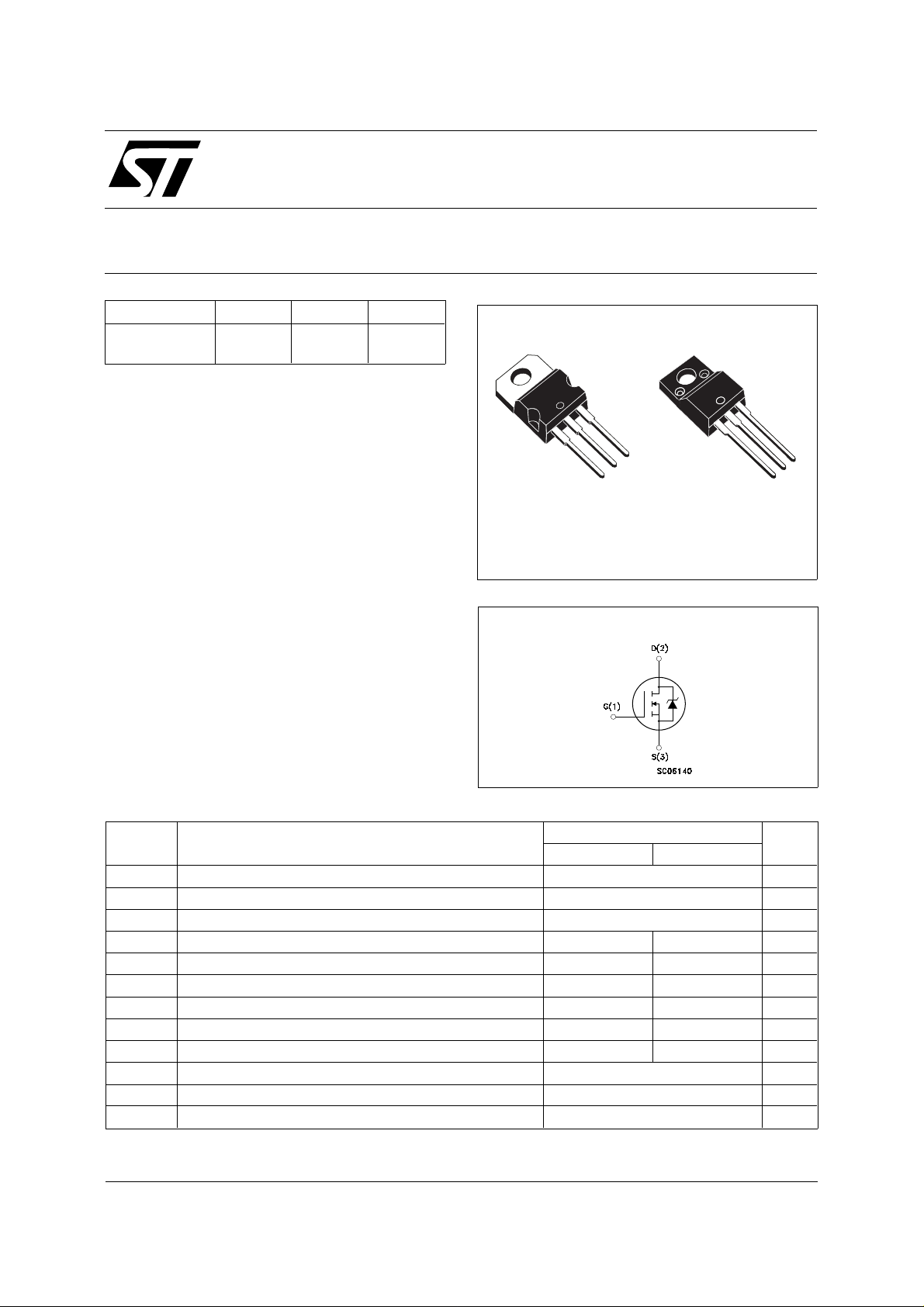
STP16NE06FP
STripFET POWER MOSFET
PRELIMINARY DATA
3
2
1
TO-220 TO-220FP
INTER NAL SCH E M ATI C DIAG RA M
3
2
1
APPLICATIONS
■ DC MOTOR CONTROL
■ DC-DC & DC-AC CONVERT E RS
■ SYNCHRONOUS RECTIFICATION
ABSOLUTE MAXIMUM RATINGS
Symbol Parameter Value Unit
STP16NE06 STP16NE06FP
V
V
V
I
DM
P
V
dV/dt Peak Diode Recovery voltage slope 6 V/ns
T
(•) Pulse width limited by safe operating area (1) ISD ≤ 16 A, di/dt ≤ 200 A/µs, VDD ≤ V
New RDS (on) spec. starting from JULY 98
’
June 1998
Drain-source Voltage (VGS = 0) 60 V
DS
Drain- gate Voltage (RGS = 20 kΩ)
DGR
Gate-source Voltage ± 20 V
GS
Drain Current (continuous) at Tc = 25 oC1611A
I
D
I
Drain Current (continuous) at Tc = 100 oC107A
D
60 V
(•) Drain Current (pulsed) 64 64 A
Total Dissipation at Tc = 25 oC6030W
tot
Derating Factor 0.4 0.2 W/
Insulation Withstand Voltage (DC) 2000 V
ISO
Storage Temperature -65 to 175
stg
Max. Operating Junction Temperature 175
T
j
, Tj ≤ T
(BR)DSS
JMAX
o
C
o
C
o
C
1/9
Page 2
STP16NE06/FP
THERMAL DATA
TO-220 TO-220FP
R
thj-case
R
thj-amb
R
thc-sink
T
AVALANCHE CHARACTERI S TICS
Symbol Parameter Max Value Unit
I
AR
E
Thermal Resistance Junction-case Max 2.5 5
Thermal Resistance Junction-ambient Max
Thermal Resistance Case-sink Typ
Maximum Lead Temperature For Soldering Purpose
l
Avalanche Current, Repetitive or Not-Repetitive
(pulse width limited by T
Single Pulse Avalanche Energy
AS
(starting T
= 25 oC, ID = IAR, V
j
ma x)
j
DD
= 25 V)
62.5
0.5
300
16 A
80 mJ
o
C/W
o
C/W
o
C/W
o
C
ELECTRICAL CHARACTERISTICS (T
= 25 oC unless otherwise specified)
case
OFF
Symbol Parameter Test Conditions Min. Typ. Max. Unit
V
(BR)DSS
Drain-source
I
= 250 µA V
D
GS
= 0
60 V
Breakdown Voltage
I
DSS
I
GSS
Zero Gate Voltage
Drain Current (V
GS
Gate-body Leakage
Current (V
DS
= 0)
= 0)
= Max Rating
V
DS
V
= Max Rating Tc = 125
DS
o
C
V
= ± 20 V
GS
1
10
± 100 nA
ON (∗)
Symbol Parameter Test Conditions Min. Typ. Max. Unit
V
GS(th)
Gate Threshold
V
= VGS ID = 250 µA
DS
234V
Voltage
R
DS(on)
Static Drain-source On
VGS = 10V ID = 8 A 0.080 0.100 Ω
Resistance
I
D(on)
On State Drain Current VDS > I
V
= 10 V
GS
D(on)
x R
DS(on)max
16 A
DYNAMIC
Symbol Parameter Test Conditions Min. Typ. Max. Unit
g
(∗) Forward
fs
Transconductance
C
C
C
Input Capacitance
iss
Output Capacitance
oss
Reverse Transfer
rss
Capacitance
VDS > I
V
DS
x R
D(on)
DS(on)max
= 25 V f = 1 MHz V
ID =8 A 6 S
30
1000
140
45
= 0 760
GS
100
µA
µA
pF
pF
pF
2/9
Page 3
STP16NE06/FP
ELECTRICAL CHARACTERISTICS (continued)
SWITCHING O N
Symbol Parameter Test Conditions Min. Typ. Max. Unit
t
d(on)
t
Q
Q
Q
SWITCHING O F F
Symbol Parameter Test Conditions Min. Typ. Max. Unit
t
r(Voff)
t
SOURCE DRAIN DIO DE
Symbol Parameter Test Conditions Min. Typ. Max. Unit
I
SD
I
SDM
V
SD
t
Q
I
RRM
(∗) Pulsed: Pulse duration = 300 µs, duty cycle 1.5 %
(•) Pulse width limited by safe operating area
Turn-on Time
Rise Time
r
Total Gate Charge
g
Gate-Source Charge
gs
Gate-Drain Charge
gd
Off-voltage Rise Time
Fall Time
t
f
Cross-over Time
c
Source-drain Current
(•)
Source-drain Current
V
= 30 V ID = 8 A
DD
R
=4.7 W VGS = 10 V
G
VDD = 40 V ID = 16 A V
V
= 48 V ID = 16 A
DD
=4.7 Ω VGS = 10 V
R
G
= 10 V 20
GS
10
35
5
7
7
18
30
80
40
30 nC
10
25
45
16
64
(pulsed)
(∗) Forward On Voltage ISD = 16 A VGS = 0 1.5 V
Reverse Recovery
rr
Time
Reverse Recovery
rr
I
= 16 A di/dt = 100 A/µs
SD
V
= 30 V Tj = 150 oC
DD
70
0.21
Charge
Reverse Recovery
6
Current
ns
ns
nC
nC
ns
ns
ns
A
A
ns
µC
A
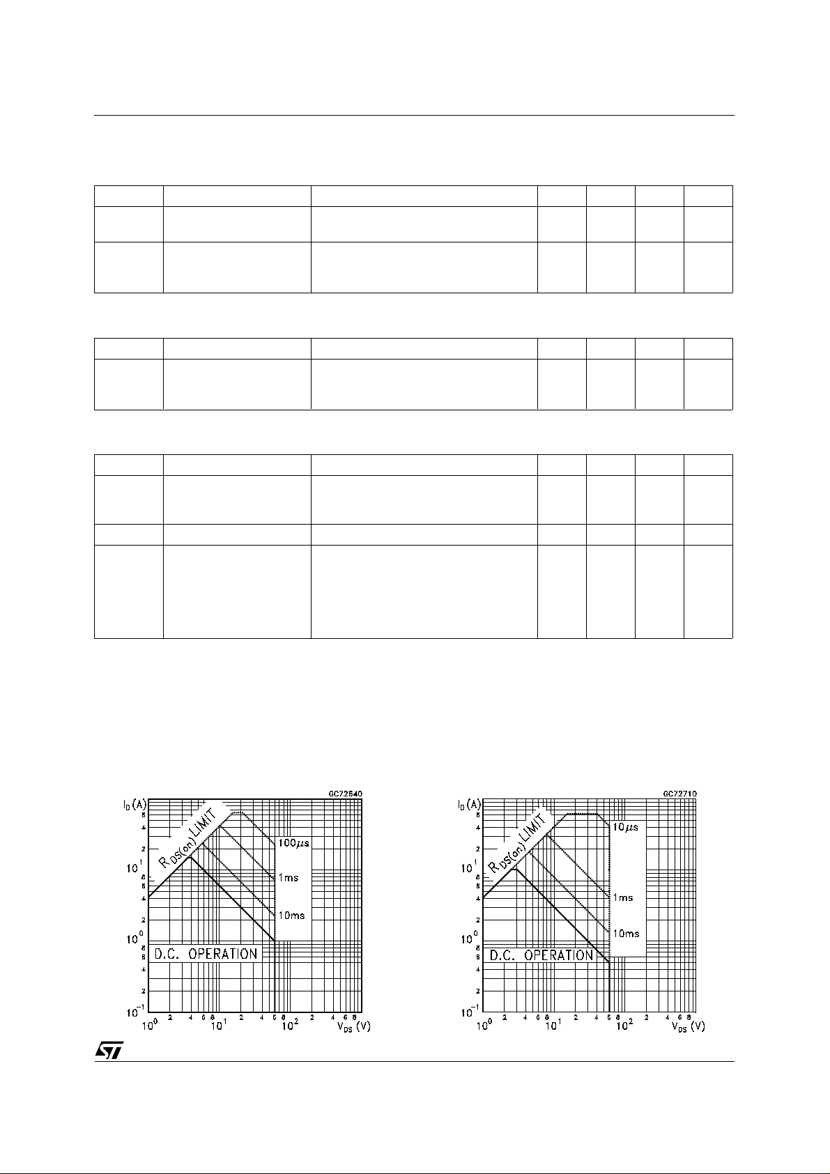
Safe Operating Area for TO-220 Safe Operating Are a for TO-220FP
3/9
Page 4

STP16NE06/FP
Thermal Impedance for TO-2 20
Output Characteris tics
Thermal Impedance for TO-220FP
Transfer Characteris tic s
Transconductance
4/9
Static Drain-source On Resist a nce
Page 5

STP16NE06/FP
Gate Charge vs Gate-source Voltage
Normalized Gate Threshold Voltage vs
Temperature
Capacitance Variations
Normalized On Resistance vs Temperature
Source-drain Diode Forward Characteris tic s
5/9
Page 6

STP16NE06/FP
Fig. 1: Unclamped Inductive Load Test Circuit
Fig. 3: Switching Tim es Test Circ uits For
Resistive Load
Fig . 2 : Unclamped Inductive Waveform
Fig. 4: Gate Charge test Circuit
Fig. 5: Test Circuit For Inductive Load Switching
And Diode Recovery Times
6/9
Page 7

E
TO-220 MECHANICAL DATA
STP16NE06/FP
DIM.
MIN. TYP. MAX. MIN. TYP. MAX.
A 4.40 4.60 0.173 0.181
C 1.23 1.32 0.048 0.051
D 2.40 2.72 0.094 0.107
D1 1.27 0.050
E 0.49 0.70 0.019 0.027
F 0.61 0.88 0.024 0.034
F1 1.14 1.70 0.044 0.067
F2 1.14 1.70 0.044 0.067
G 4.95 5.15 0.194 0.203
G1 2.4 2.7 0.094 0.106
H2 10.0 10.40 0.393 0.409
L2 16.4 0.645
L4 13.0 14.0 0.511 0.551
L5 2.65 2.95 0.104 0.116
L6 15.25 15.75 0.600 0.620
L7 6.2 6.6 0.244 0.260
L9 3.5 3.93 0.137 0.154
DIA. 3.75 3.85 0.147 0.151
mm inch
A
C
D
D1
L2
F1
L5
Dia.
G1
F
F2
L9
G
H2
L7
L6
L4
P011C
7/9
Page 8

STP16NE06/FP
TO-220FP MECHANICAL DAT A
DIM.
MIN. TYP. MAX. MIN. TYP. MAX.
A 4.4 4.6 0.173 0.181
B 2.5 2.7 0.098 0.106
D 2.5 2.75 0.098 0.108
E 0.45 0.7 0.017 0.027
F 0.75 1 0.030 0.039
F1 1.15 1.7 0.045 0.067
F2 1.15 1.7 0.045 0.067
G 4.95 5.2 0.195 0.204
G1 2.4 2.7 0.094 0.106
H 10 10.4 0.393 0.409
L2 16 0.630
L3 28.6 30.6 1.126 1.204
L4 9.8 10.6 0.385 0.417
L6 15.9 16.4 0.626 0.645
L7 9 9.3 0.354 0.366
Ø 3 3.2 0.118 0.126
mm inch
A
B
H
E
D
L3
L6
L7
¯
F1
F
G1
G
F2
123
L2
L4
8/9
Page 9

STP16NE06/FP
Information furnished is believed to be accurate and reliable. However, STMicroelectronics assumes no responsibility for the consequences
of use of such inform ation nor for any infringe ment o f patents or other rig hts o f third par ties which ma y resul t from i ts use. N o li cen se is
granted by implicatio n or otherwise under any patent or patent rights of STMicroelectronics. Specification mentioned in this publication are
subject to change without notice. This publication supersedes and replac es all information previously supplied. STMicroelectronics products
are not authorized for use as critical compo nents in life support devices or systems without express written approval of STMicroelectronics.
The ST logo is a trademark of STMicroelectronics
© 1998 STMicroelectro nics – Printed in Italy – All Rights Reserved
STMicroelectronics GROUP OF COMPANIES
Australia - Brazil - Canada - China - France - Germany - Italy - Japan - Korea - Malaysia - Malta - Morocco - The Netherlands -
Singapore - Spain - Sweden - Switzerland - Taiwan - Thailand - United Kingdom - U.S.A.
.
9/9
 Loading...