

Page 1
查询STP16CP596供应商
STP16CP596
LOW VOLTAGE 16-BIT CONSTANT
CURRENT LED SINK DRIVER
■ LOW VOLTAGE POWER SUPPLY DOWN T O
3V
■ 16 CONSTANT CURRENT OUTPUT
CHANNELS
■ ADJUST ABLE OUTPUT CURRENT
THROUGH EXTERNAL RESISTOR
■ SERIAL DATA IN/PARALLEL DATA OUT
■ SERIAL OUT CHANGES STATE ON THE
FALLING E DGES OF CLOCK
■ 3.3V MICRO DRIVER-ABLE
■ OUTPUT CURRENT : 3-50 mA
■ 25 MHz CLOCK FREQ.
■ A V AILABL E IN HIGH T HERMAL EFFI CIENCY
TSSOP EXPOSED PAD
DESCRIPTION
The STP16CP596 is a monolithic, low voltage, low
current power 16-bit shift register designed for
LED panel displays. The STP16CP596 contains a
16-bit serial-in, parallel-out shift register that feeds
a 16-bitD-type storage register. In the output
stage, sixteen regulated current sources were
designed to provide 3-50mA constant current to
drive the LEDs.
Compared with the STPIC6C595, the device
provides great flexibility and improved
performance in LED panel system design.
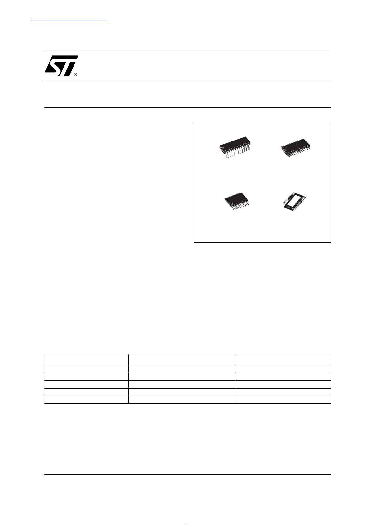
DIP-24
TSSOP24
SO-24
TSSOP24
(exposed pad)
Trough an external resistor, users can adjust the
STP16CP596 output current, controlling in this
way the light intensity of LEDs.
The STP16CP596 guarantees a 16V output
driving capability, allowing users to connect more
LEDs in series. The high clock frequency, 25 MHz,
also satisfies the system requirement of high
volume data transmission. The 3.3V of voltage
supply is well useful for applications that in terface
any micro from 3.3V. Compared w ith a standard
TSSOP package, the TSSOP exposed pad
increases heat dissipation capability by a 2.5
factor.
Table 1: Order Codes
Type Package Comments
STP16CP596B1R DIP-24 15 parts per tube
STP16CP596M SO-24 (Tube) 40 parts per tube
STP16CP596MTR SO-24 (Tape & Reel) 1000 parts per reel
STP16CP596TTR TSSOP24 (Tape & Reel) 2500 parts per reel
STP16CP596XTTR TSSOP24 Exposed-Pad (Tape & Reel) 2500 parts per reel
Rev. 3
1/18July 2005
Page 2
STP16CP596
Table 2: Typical Current Accuracy
Output Voltage Output Current Between Bits Between ICs
≥ 0.1V
≥ 0.15V
≥ 0.25V
≥ 0.5V
≥ 1.2V
≥ 1.4V
3 mA/V
5 mA/V
10 mA/V
20 mA/V
40 mA/V
50 mA/V
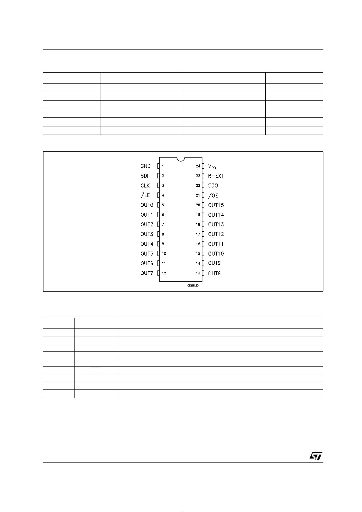
Figure 1: Pin Connection (Note 1)
CC
CC
CC
CC
CC
CC
= 5V
= 5V
= 5V
= 5V
= 5V
= 5V
± 3% ± 6%
± 2% ± 6%
± 2% ± 6%
± 1% ± 6%
± 1% ± 6%
± 1% ± 6%
Note 1: The exposed Pad is electrically no t c onnected.
Table 3: Pin Description
PIN N° Symbol Name and Function
1 GND Ground Terminal
2 SDI Serial data input terminal
3 CLK Clock input terminal
4 /LE Latch input terminal
5-20 OUT 0-15 Output terminal
21 /OE
22 SDO Serial data out terminal
23 R-EXT Input terminal of an external resistor for constant current programing
24 V
DD
2/18
Input terminal of output enable (active low)
Supply voltage terminal
Page 3
STP16CP596
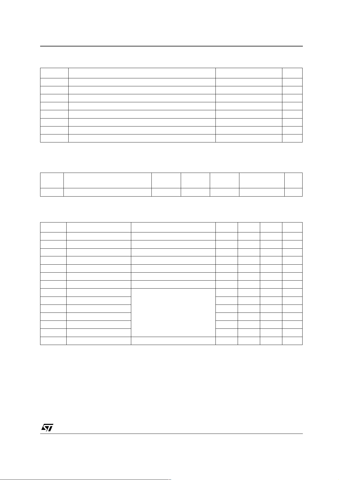
Table 4: Absolute Maximum Ratings
Symbol Parameter Value Unit
V
V
I
V
I
GND
f
CLK
T
OPR
T
STG
Absolute Maximum Ra tings are those v al ues beyond which damage to the device may occur. Under the se conditions, functional operation
is not implied.
Table 5: Thermal Data
Supply Voltage
DD
Output Voltage
O
Output Current
O
Input Voltage -0.4 to VDD+0.4
I
GND Terminal Current
Clock Frequency
Operating Temperature Range
Storage Temperature Range
0 to 7 V
-0.5 to 16 V
50 mA
V
800 mA
25 MHz
-40 to +125 °C
-65 to +150 °C
Symbol Parameter DIP-24 SO-24 TSSOP24
R
thj-amb
(*) The exposed pad shou l d be soldered directly to the PCB to realize the th ermal benefits.
Thermal Resistance Junction-ambient
60 75 85 37.5 °C/W
TSSOP24 (*)
(exposed pad)
Table 6: Recommended Operating Conditions
Symbol Parameter Test Conditions Min. Typ. Max. Unit
V
V
I
I
V
V
t
wLAT
t
wCLK
t
wEN
t
SETUP(D)
t
HOLD(D)
t
REM(L)
f
CLK
Supply Voltage 3.0 5.5 V
DD
Output Voltage 16.0 V
O
Output Current OUTn 3 50 mA
I
O
Output Current SERIAL-OUT +1 mA
OH
Output Current SERIAL-OUT -1 mA
OL
Input Voltage 0.7V
IH
Input Voltage -0.3 0.3V
IL
DD
/LE Pulse Width VDD = 3.0 to 3.6V 20 ns
CLK Pulse Width 20 ns
/OE Pulse Width 400 ns
Setup Time for DATA 20 ns
Hold Time for DATA 15 ns
Removal Time for LATCH 15 ns
Clock Frequency Cascade Operation 25 MHz
VDD+0.3 V
DD
Unit
V
3/18
Page 4
STP16CP596
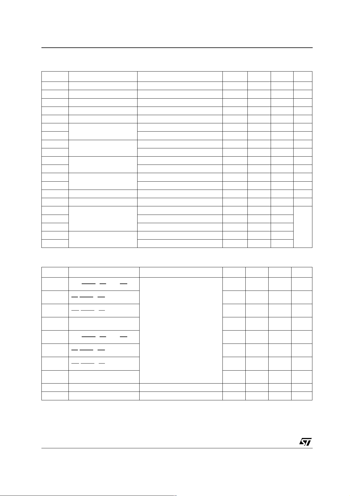
Table 7: Electrical Characteristics (VDD=3.3V to 5V, T = 25°C, unless otherwise specified.)
Symbol Parameter Test Conditions Min. Typ. Max. Unit
V
V
I
V
V
I
OL1A
I
OL2A
∆I
OL1A
∆I
OL2A
I
OL1B
I
OL2B
∆I
OL1B
∆I
OL2B
R
SIN(up)
R
SIN(down)
I
DD(OFF1)
I
DD(OFF2)
I
DD(OFF3)
I
DD(ON1)
I
DD(ON2)
Input Voltage High Level 0.7V
IH
Input Voltage Low Level GND 0.3V
IL
Output Leakage Current VOH = 16 V 10 µA
OH
Output Voltage (Serial-OUT) IOL = 1mA 0.4 V
OL
Output Voltage (Serial-OUT) IOH = -1mA VDD-0.4V V
OH
Output Current VO = ≥0.2V, R
VO = ≥0.5V, R
Output Current Error
between bit (All Output ON)
VO = ≥0.2V, R
VO = ≥0.5V, R
Output Current VO = ≥0.2V, R
VO = ≥0.5V, R
Output Current Error
between bit (All Output ON)
VO = ≥0.2V, R
VO = ≥0.5V, R
=6.2KΩ, VDD=3.3V 2.85 3 3.15 mA
EXT
=1KΩ, VDD = 3.3V 19.6 20 20.4 mA
EXT
=6.2KΩ, VDD=3.3V ± 4 ± 6 %
EXT
=1KΩ, VDD = 3.3V ± 2 ± 3 %
EXT
=6.2KΩ, VDD=5V 2.9 3 3.1 mA
EXT
=1KΩ, VDD = 5V 19.6 20 20.4 mA
EXT
=6.2KΩ, VDD=5V ± 2 ± 3.5 %
EXT
=1KΩ, VDD = 5V ± 1 ± 2 %
EXT
DD
Pull-up Resistor 150 300 600 KΩ
Pull-down Resistor 100 200 400 KΩ
Supply Current (OFF) R
Supply Current (ON) R
= OPEN OUT 0 to 15 = OFF 0.3 mA
EXT
R
= 6.2KΩ OUT 0 to 15 = OFF 1
EXT
R
= 1KΩ OUT 0 to 15 = OFF 3
EXT
= 6.2KΩ OUT 0 to 15 = ON 1
EXT
R
= 1KΩ OUT 0 to 15 = ON 3
EXT
V
DD
DD
V
V
Table 8: Switching Characteristics (V
=3V, T = 25°C, unless otherwise specified.)
DD
Symbol Parameter Test Conditions Min. Typ. Max. Unit
t
PLH1
t
PLH2
t
PLH3
t
PLH
t
PHL1
t
PHL2
t
PHL3
t
PHL
t
ON
t
OFF
Propagation Delay Time,
CLK-OUTn
, /LE = H, /OE = L
Propagation Delay Time,
-OUTn, /OE = L
/LE
Propagation Delay Time,
-OUTn, /LE = H
/OE
V
= 3 V VIH = V
DD
DD
VIL = GND CL = 13pF
= 40mA VL = 3 V
I
O
R
= 470 Ω RL = 65 Ω
EXT
Propagation Delay Time,
CLK-SDO
Propagation Delay Time,
CLK-OUTn, /LE = H, /OE = L
Propagation Delay Time,
-OUTn, /OE = L
/LE
Propagation Delay Time,
-OUTn, /LE = H
/OE
Propagation Delay Time,
CLK-SDO
Output Rise Time 10 ~ 90% of voltage waveform 260 400 ns
Output Fall Time 90 ~ 10% of voltage waveform 50 80 ns
250 280 ns
220 250 ns
200 250 ns
25 50 ns
25 50 ns
25 50 ns
50 70 ns
25 50 ns
4/18
Page 5
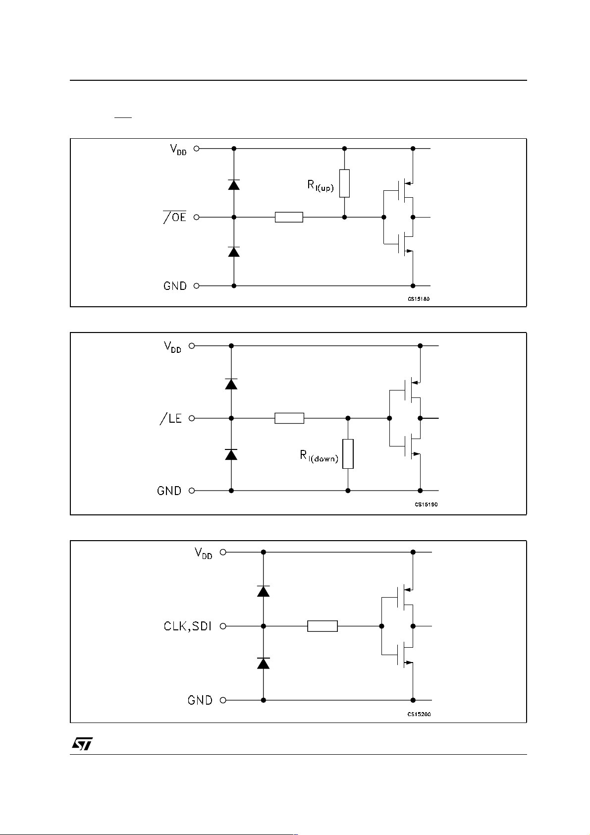
EQUIVALENT CIRCUIT OF INPUTS AND OUTPUTS
STP16CP596
Figure 2: /OE
Figure 3: /LE Terminal
Terminal
Figure 4: CLK, SDI Terminal
5/18
Page 6
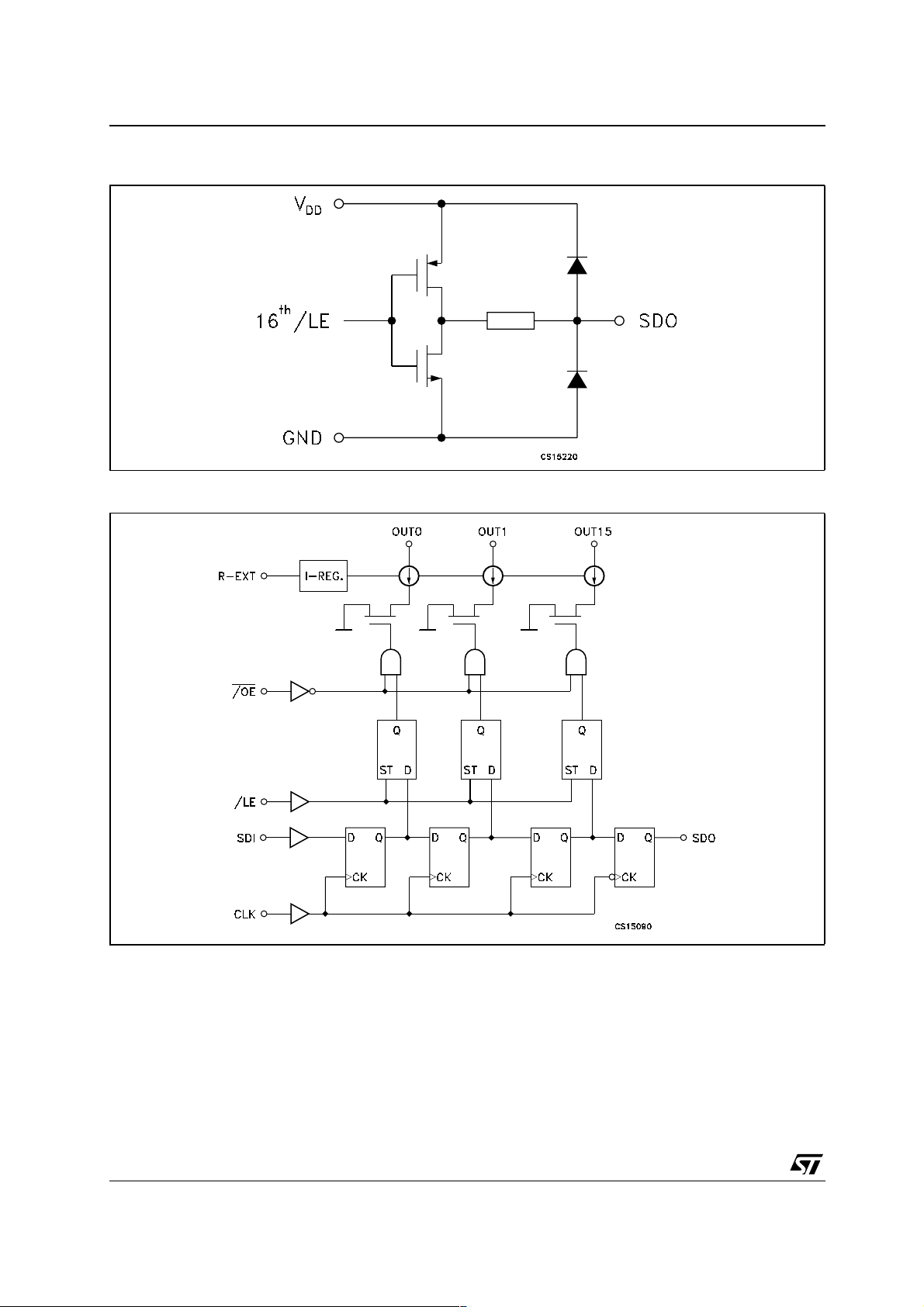
STP16CP596
Figure 5: SDO Terminal
Figure 6: Block Diagram
6/18
Page 7
STP16CP596
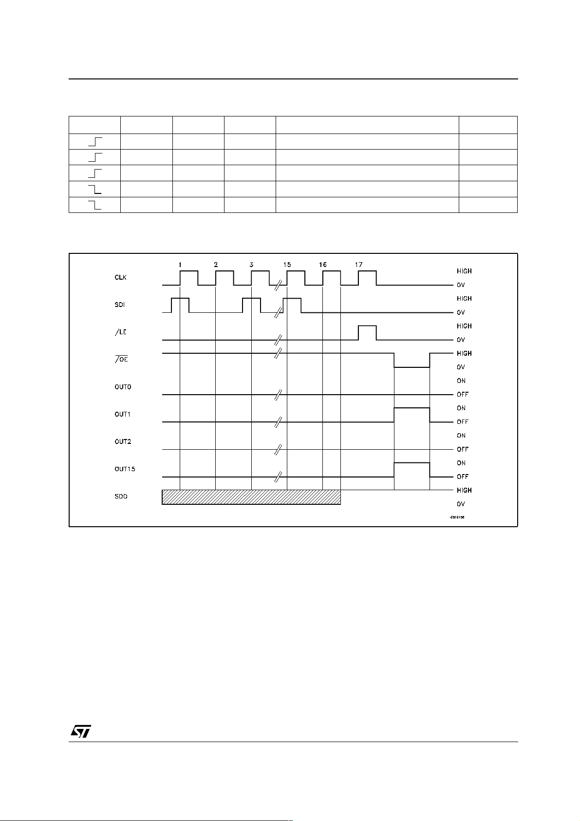
Table 9: Truth Tabl e
CLOCK /LE /OE SERIAL-IN OUT0 .................. OUT7 .................. OUT15 SDO
H L Dn Dn ..... Dn - 7 ..... Dn -15 Dn - 15
L L Dn + 1 No Change Dn - 14
H L Dn + 2 Dn - 2 ..... Dn - 5 ..... Dn -13 Dn - 13
X L Dn + 3 Dn - 2 ..... Dn - 5 ..... Dn -13 Dn - 13
XLDn + 3 OFF Dn - 13
Note 1: OUT0 to OUT15 = ON when Dn = H; OUT0 to OUT15 = OFF when Dn = L.
Figure 7: Timi ng Diagram
Note: The latches ci rc uit holds da ta when the LE termi n a l is Low.
When LE terminal is at High l evel, latch circuit doesn’ t ho l d the data it passes from the inpu t to the output.
When OE terminal is at Low level, output terminals OUT0 to OUT15 respond to the data, either ON or OFF.
When OE terminal is at High level, it switches off all the data on the output terminal.
7/18
Page 8
STP16CP596
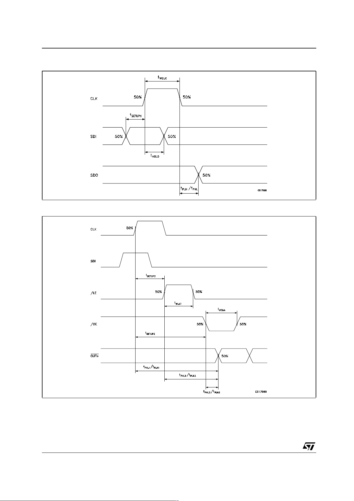
Figure 8: Clock, Serial-in, Serial-out
Figure 9: Clock, Serial-in, Latch, Enable, Outputs
8/18
Page 9
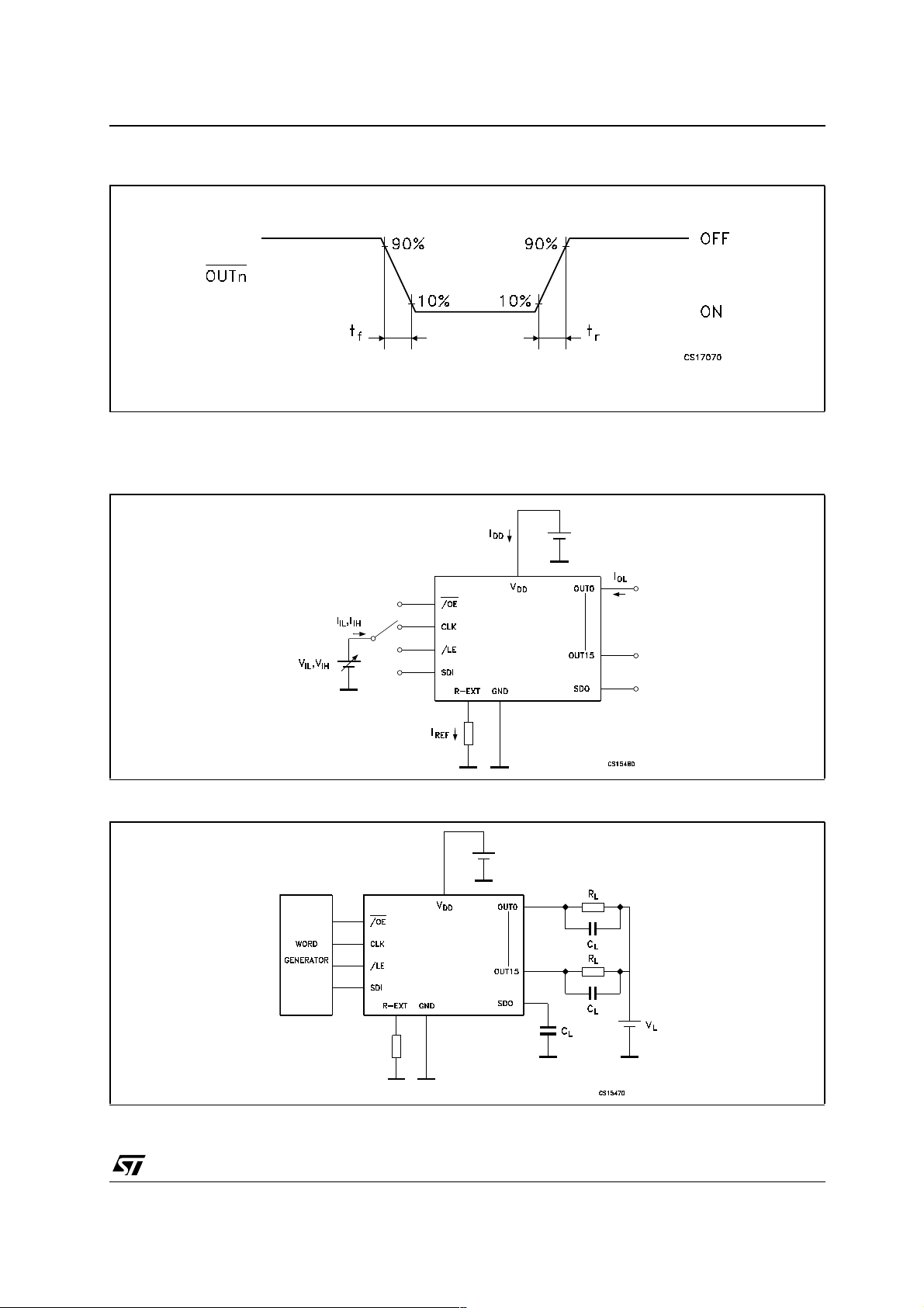
Figure 10: Outp uts
TEST CIRCUIT
Figure 11: DC Characteristic
STP16CP596
Figure 12: AC Characteristic
9/18
Page 10
STP16CP596
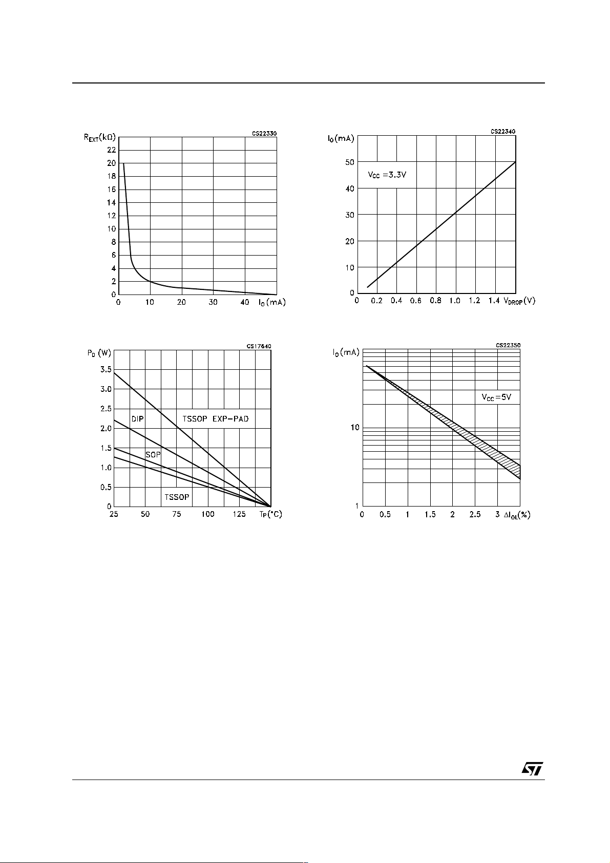
Figure 13: Output Current-R
Resistor
EXT
Figure 14: Power Dissipation vs Temperature
Package
Figure 15: Output Current vs Dropout Voltage
Figure 16: Output Current vs ±∆I
OL
(%)
10/18
Page 11
STP16CP596
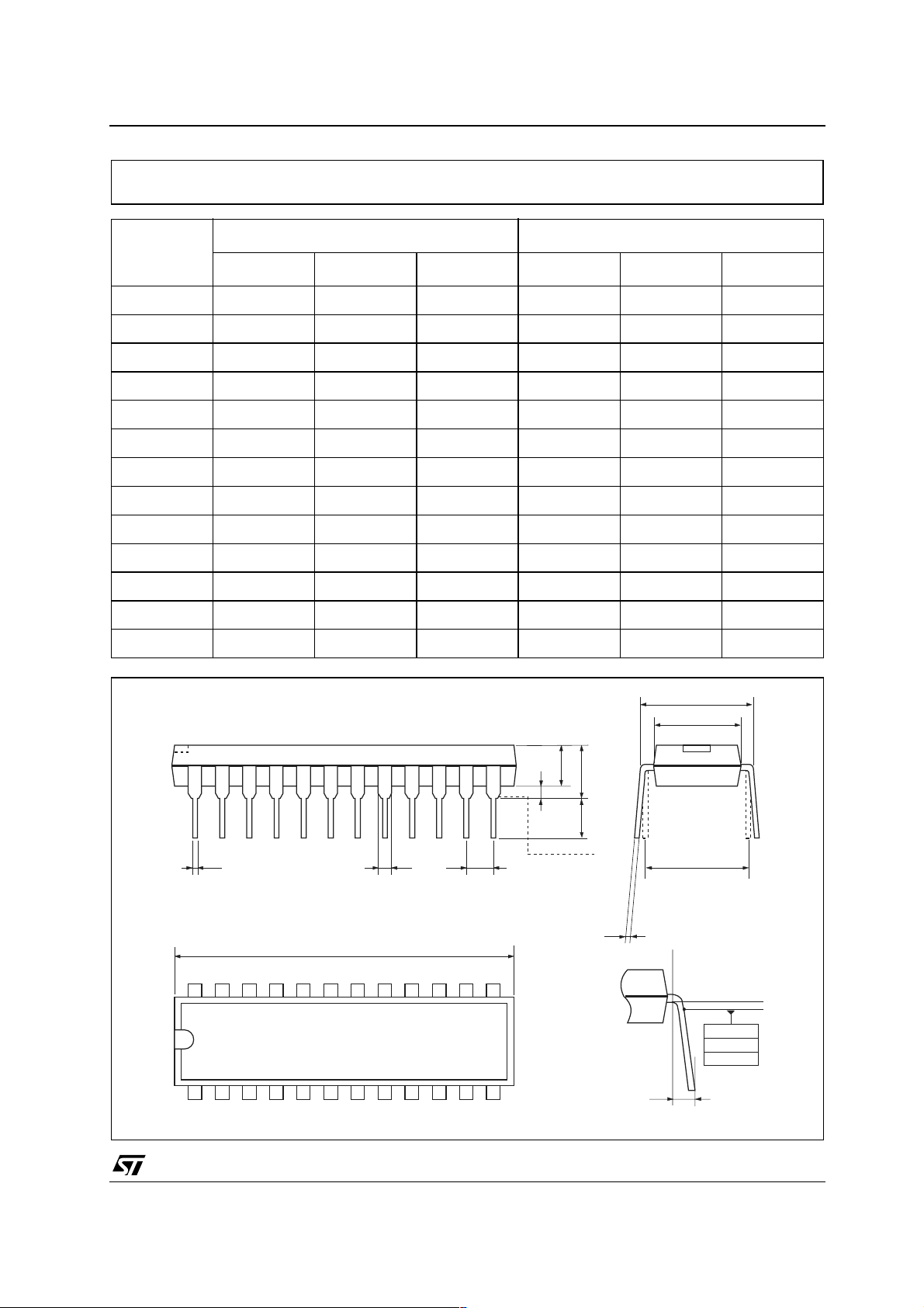
Plastic DIP-24 (0.25) MECHANICAL DATA
mm. inch
DIM.
MIN. TYP MAX. MIN. TYP. MAX.
A 4.32 0.170
A1 0.38 0.015
A2 3.3 0.130
B 0.41 0.46 0.51 0.016 0.018 0.020
B1 1.40 1.52 1.65 0.055 0.060 0.065
c 0.20 0.25 0.30 0.008 0.010 0.012
D 31.62 31.75 31.88 1.245 1.250 1.255
E 7.62 8.26 0.300 0.325
E1 6.35 6.60 6.86 0.250 0.260 0.270
e 2.54 0.100
E1 7.62 0.300
L 3.18 3.43 0.125 0.135
M 0˚ 15˚ 0˚ 15˚
E
E1
A2
A1
LA
B eB1
D
24
1
13
12
Stand-off
e1
c
.015
0,38
Gage Plane
M
0034965/D
11/18
Page 12
STP16CP596
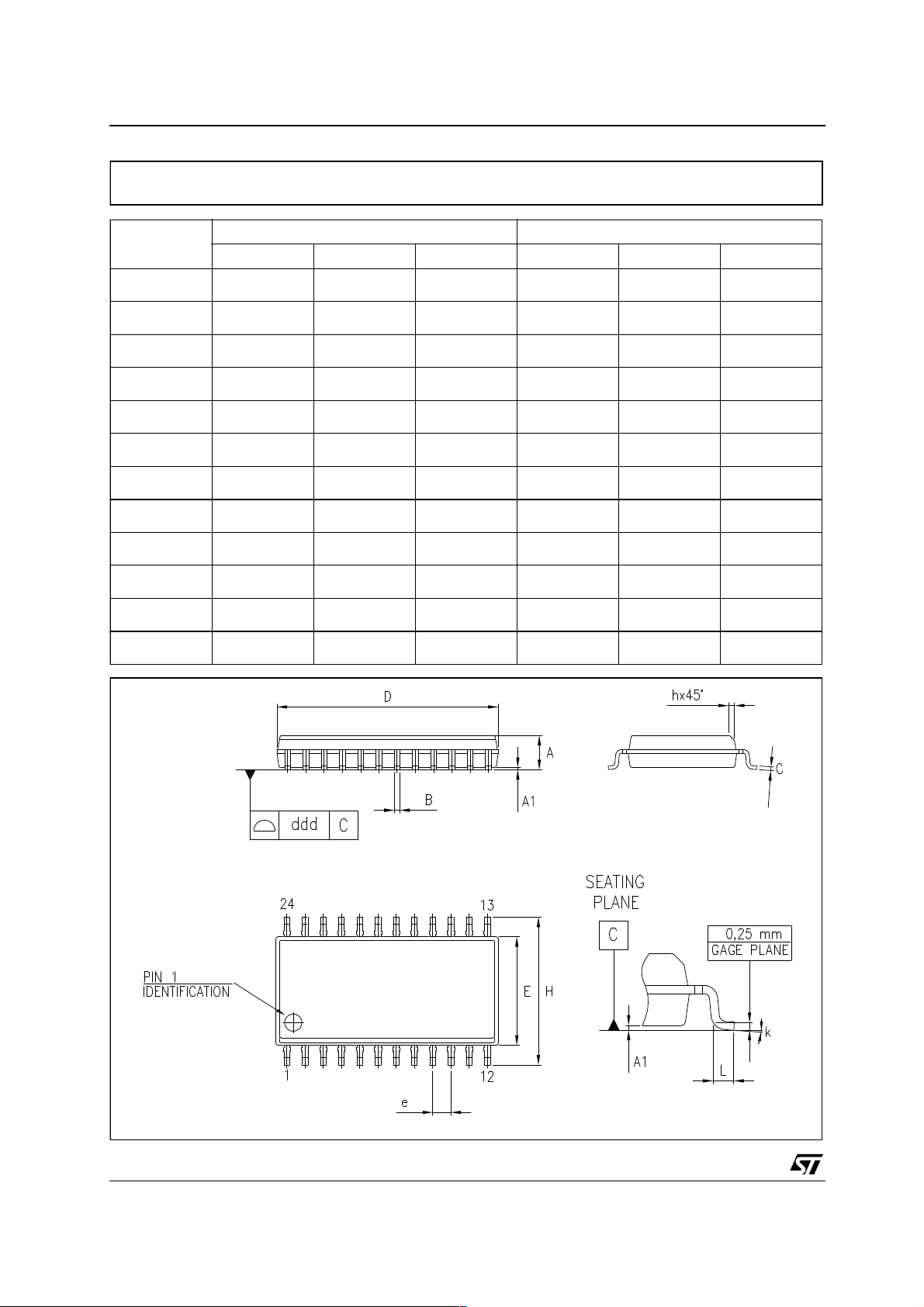
SO-24 MECHANICAL DATA
DIM.
A 2.35 2.65 0.093 0.104
A1 0.1 0.30 0.004 0.012
B 0.33 0.51 0.013 0.020
C 0.23 0.32 0.009 0.013
D 15.20 15.60 0.598 0.614
E 7.4 7.6 0.291 0.299
e 1.27 0.050
H 10.00 10.65 0.394 0.419
h 0.25 0.75 0.010 0.030
L 0.4 1.27 0.016 0.050
k0° 8° 0° 8°
ddd 0.100 0.004
MIN. TYP MAX. MIN. TYP. MAX.
mm. inch
12/18
0070769C
Page 13
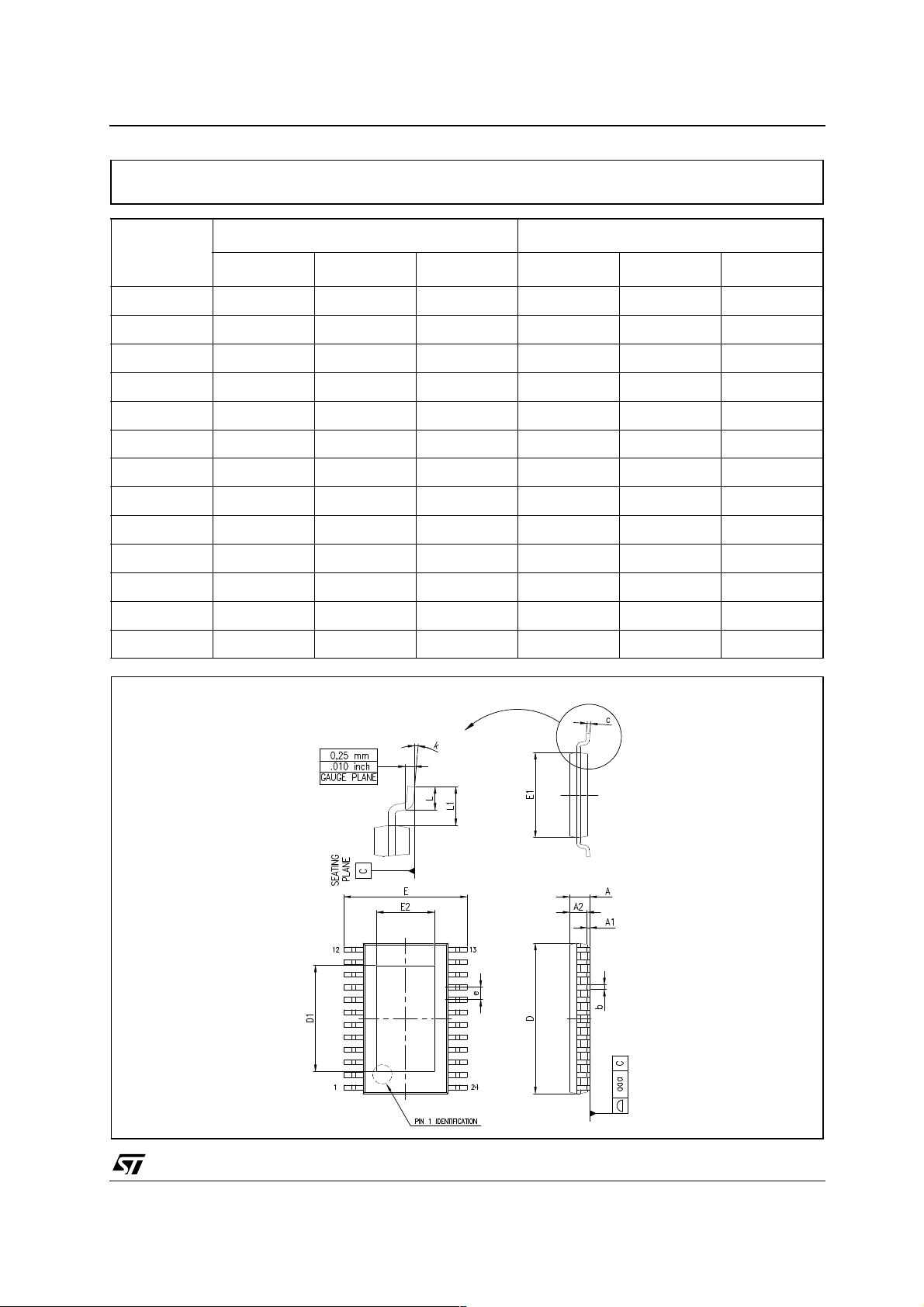
STP16CP596
TSSOP24 EXPOSED PAD MECHANICAL DATA
mm. inch
DIM.
MIN. TYP MAX. MIN. TYP. MAX.
A 1.2 0.047
A1 0.15 0.004 0.006
A2 0.8 1 1.05 0.031 0.039 0.041
b 0.19 0.30 0.007 0.012
c 0.09 0.20 0.004 0.0089
D 7.7 7.8 7.9 0.303 0.307 0.311
D1 2.7 0.106
E 6.2 6.4 6.6 0.244 0.252 0.260
E1 4.3 4.4 4.5 0.169 0.173 0.177
E2 1.5 0.059
e 0.65 0.0256
K0° 8° 0° 8°
L 0.45 0.60 0.75 0.018 0.024 0.030
7100778C
13/18
Page 14
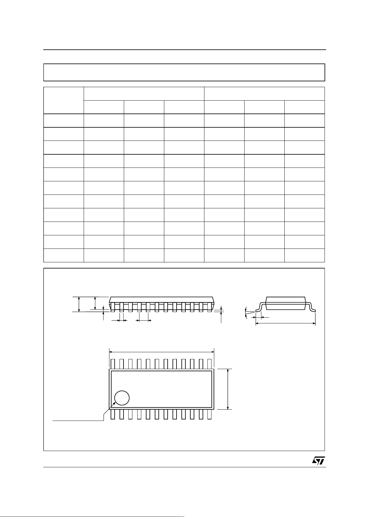
STP16CP596
TSSOP24 MECHANICAL DATA
mm. inch
DIM.
MIN. TYP MAX. MIN. TYP. MAX.
A 1.1 0.043
A1 0.05 0.15 0.002 0.006
A2 0.9 0.035
b 0.19 0.30 0.0075 0.0118
c 0.09 0.20 0.0035 0.0079
D 7.7 7.9 0.303 0.311
E 4.3 4.5 0.169 0.177
e 0.65 BSC 0.0256 BSC
H 6.25 6.5 0.246 0.256
K0° 8° 0° 8°
L 0.50 0.70 0.020 0.028
A2
A
A1
b
e
D
K
c
E
L
H
PIN 1 IDENTIFICATION
14/18
1
7047476B
Page 15
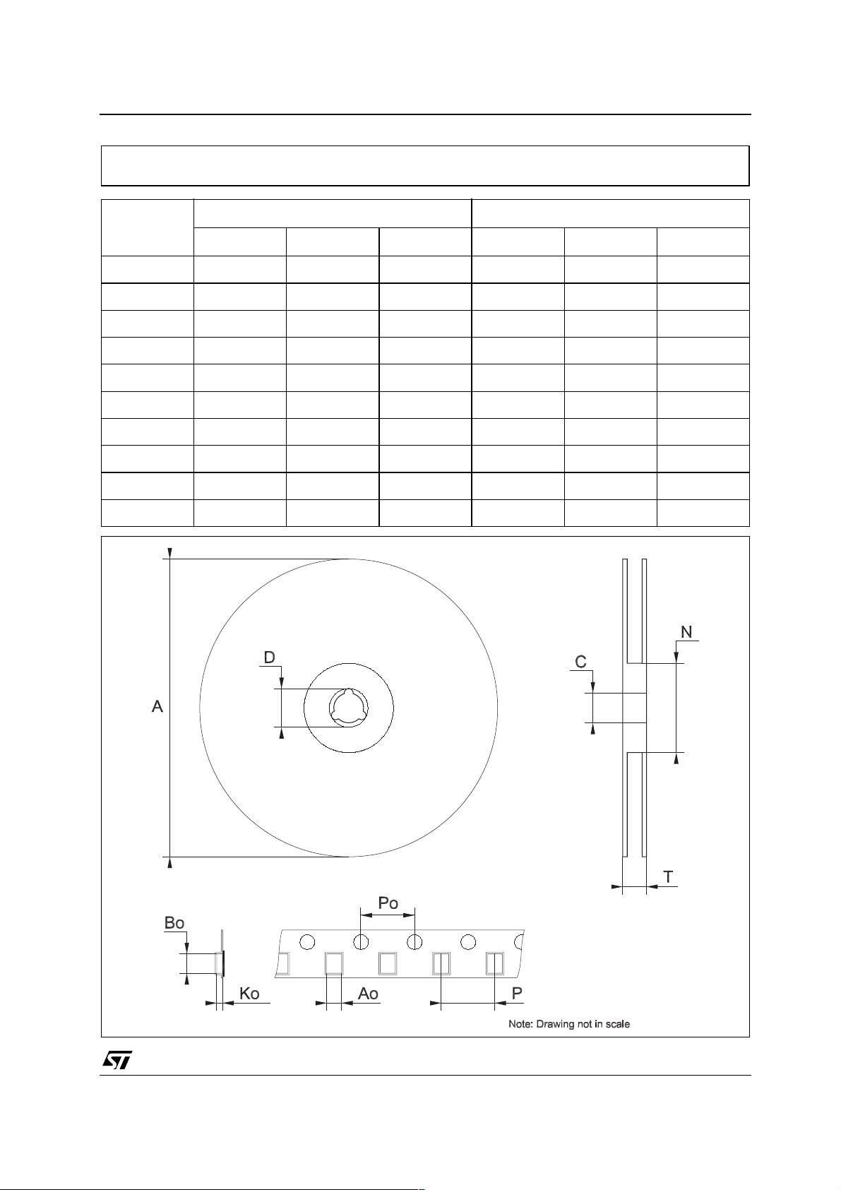
STP16CP596
Tape & Reel SO-24 MECHANICAL DATA
mm. inch
DIM.
MIN. TYP MAX. MIN. TYP. MAX.
A 330 12.992
C 12.8 13.2 0.504 0.519
D 20.2 0.795
N 60 2.362
T 30.4 1.197
Ao 10.8 11.0 0.425 0.433
Bo 15.7 15.9 0.618 0.626
Ko 2.9 3.1 0.114 0.122
Po 3.9 4.1 0.153 0.161
P 11.9 12.1 0.468 0.476
15/18
Page 16
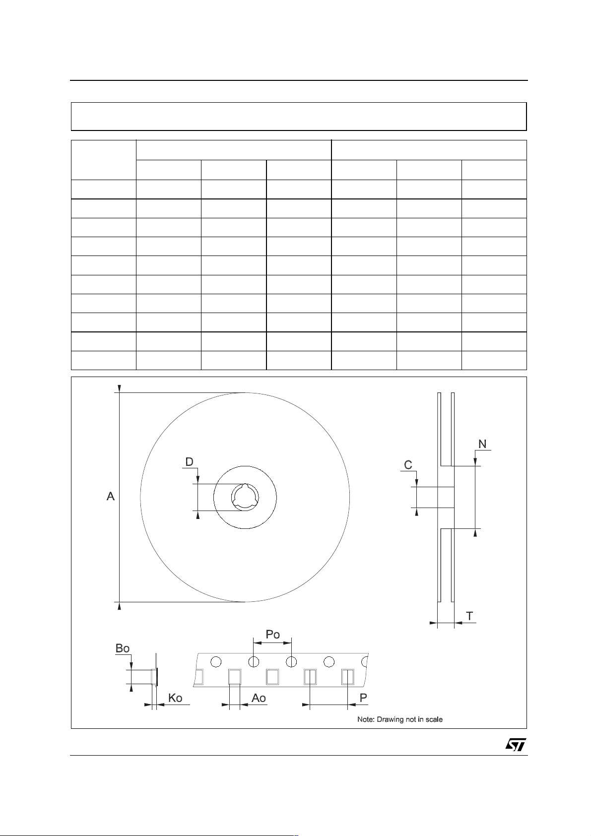
STP16CP596
Tape & Reel TSSOP24 MECHANICAL DATA
mm. inch
DIM.
MIN. TYP MAX. MIN. TYP. MAX.
A 330 12.992
C 12.8 13.2 0.504 0.519
D 20.2 0.795
N 60 2.362
T 22.4 0.882
Ao 6.8 7 0.268 0.276
Bo 8.2 8.4 0.323 0.331
Ko 1.7 1.9 0.067 0.075
Po 3.9 4.1 0.153 0.161
P 11.9 12.1 0.468 0.476
16/18
Page 17
Table 10: Revision History
Date Revision Description of Changes
08-Apr-2005 1 First Release.
02-May-2005 2 Typing Error on the description features.
25-Jul-2005 3 Add note on Fig. 1 and Table 5.
STP16CP596
17/18
Page 18

STP16CP596
Information furnished is believed to be accurate and reliable. However, STMicroelectronics assumes no responsibility for the consequences
of use of such information nor for any infringement of patents or other rights of third parties which may result from its use. No license is granted
by implic ati o n or ot h er wis e und er an y pat ent or pa te nt r igh ts of STMi cr oe l ect ro ni cs . Sp ec if i cat i on s ment i o ned i n th is p ub li c ati on ar e s ubj ec t
to change without notice. This publication supersedes and replac es all information previously supplied. STMicroelectronics product s are not
authorized for use as critical components in life support devices or systems without express written approval of STMicroelectronics.
The ST logo is a registered trademark of STMicroelectronics
All other names are the property of their respective owners
© 2005 STMicroelectronics - All Rights Reserved
STMicroelectronics group of companies
Australia - Belgium - Brazil - Canada - China - Czech Republic - Finland - France - Germany - Hong Kong - India - Israel - Italy - Japan -
Malaysia - Malta - Morocco - Singapore - Spain - Sweden - Switzerland - United Kingdom - United States of America
www.st.com
18/18
 Loading...