

Page 1
STB14NF10
STP14NF10 STP14NF10FP
N-CHANNEL 100V - 0.115 Ω - 15A TO-220/TO-220FP/D2PAK
LOW GATE CHARGE STripFET™ II POWER MOSFET
TYPE
STB14NF10
STP14NF10
STP14NF10FP
■ TYPICAL R
■ EXCEPTIONA L dv/d t CAPABILITY
■ 100% AVALANCHE TESTED
■ APPLICATION ORIENTED
V
DSS
100 V
100 V
100 V
(on) = 0.115 Ω
DS
R
DS(on)
<0.13
<0.13
<0.13
I
D
15 A
Ω
15 A
Ω
10 A
Ω
CHARACTERIZATION
■ SURFACE-MOUNTING D
2
PAK (TO-263)
POWER PACKAG E IN TU BE (NO SU FFIX) OR
IN TAPE & REEL (SUFFIX “T4”)
DESCRIPTION
This MOSFET series realized with STMicroelectronics
unique STripFET™ process has specifically been designed to minimiz e inpu t capa citanc e and gate c harge . It
is therefore su itable as p rima ry sw itch i n ad vanced hig hefficiency, high-frequency isolate d DC-DC c onverters for
T elecom and Computer applications. It is also intended for
any applications with low gate drive requirements.
APPLICATIONS
■ HIGH-EFFICIENCY DC-DC CONVERTERS
■ UPS AND MOTOR CONTROL
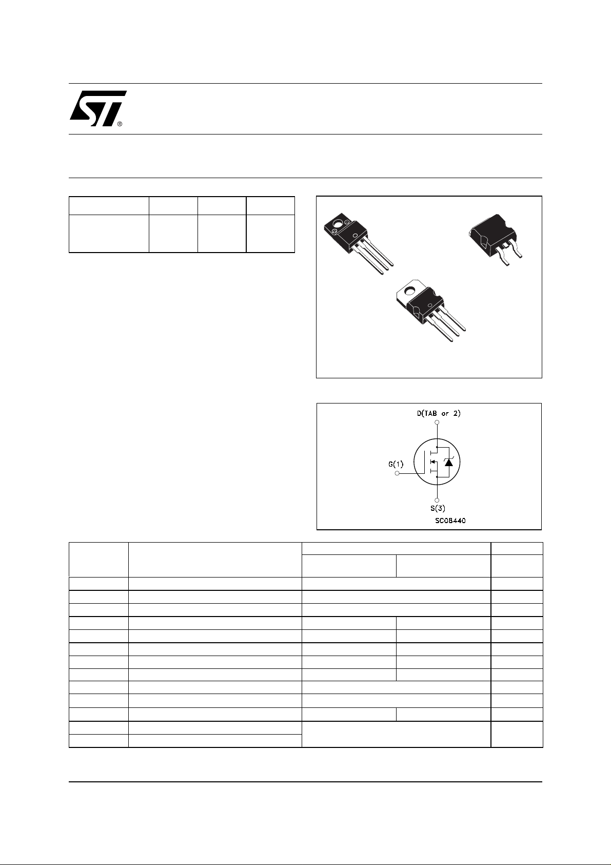
3
2
1
TO-220FP
3
2
1
TO-220
INTERNAL SCHEMATIC DIAGRAM
1
D2PAK
TO-263
(Suffix “T4”)
3
ABSOLUTE MAXIMUM RATINGS
Symbol Parameter Value Unit
STB14NF10
STP14NF10
Drain-source Voltage (VGS = 0)
Drain-gate Voltage (RGS = 20 kΩ)
Gate- source Voltage ± 20 V
Drain Current (continuous) at TC = 25°C
Drain Current (continuous) at TC = 100°C
•)
Drain Current (pulsed) 60 40 A
Total Dissipation at TC = 25°C
15 10 A
10 6.3 A
60 25 W
V
I
V
V
DM
P
DS
DGR
GS
I
D
I
D
(
tot
Derating Factor 0.4 0.17 W/°C
(1)
dv/dt
E
AS
V
ISO
T
stg
T
j
(
Pulse width l i mited by safe operating area . (1) ISD ≤14A, di/dt ≤300A/ µ s , VDD ≤ V
•)
.
Peak Diode Recovery voltage slope 9 V/ns
(2)
Single Pulse Avalanche Energy 70 mJ
Insulation Withstand Voltage (DC) ------ 2000 V
Storage Temperature
Operating Junction Temperature
(2) Starting Tj = 25 oC, ID = 15A, VDD= 50V
-55 to 175 °C
STP14NF10FP
100 V
100 V
, Tj ≤ T
(BR)DSS
JMAX
1/11June 2002
Page 2
STB14NF10 STP14NF10 STP14NF10FP
THERMA L D ATA
D2PAK
TO-220
Rthj-case Thermal Resistance Junction-case Max 2.5 6 °C/W
TO-220FP
Rthj-amb
T
ELECTRICAL CHARACTERISTICS (T
Thermal Resistance Junction-ambient
Maximum Lead Temperature For Soldering Purpose
l
= 25 °C unless otherwise specified)
case
Max 62.5
300
OFF
Symbol Parameter Test Conditions Min. Typ. Max. Unit
I
= 250 µA, VGS = 0
D
V
= Max Rating
DS
V
= Max Rating TC = 125°C
DS
V
= ± 20 V
GS
100 V
1
10
±100 nA
ON
V
(BR)DSS
I
DSS
I
GSS
(*)
Drain-source
Breakdown Voltage
Zero Gate Voltage
Drain Current (V
GS
Gate-body Leakage
Current (V
DS
= 0)
= 0)
Symbol Parameter Test Conditions Min. Typ. Max. Unit
V
GS(th)
R
DS(on)
Gate Threshold Voltage
Static Drain-source On
= VGS I
DS
V
= 10 V ID = 7 A
GS
= 250 µA
D
234V
0.115 0.13
V
Resistance
DYNAMIC
Symbol Parameter Test Conditions Min. Typ. Max. Unit
(*)
g
fs
C
iss
C
oss
C
rss
Forward Transconductance
Input Capacitance
Output Capacitance
Reverse Transfer
Capacitance
V
= 15 V ID=7 A
DS
= 25V, f = 1 MHz, VGS = 0
V
DS
20 S
460
70
30
°C/W
°C
µA
µA
Ω
pF
pF
pF
2/11
Page 3
STB14NF10 STP14NF10 STP14NF10FP
ELECTRICAL CHARACTERISTICS (continued)
SWITCHING ON
Symbol Parameter Test Conditions Min. Typ. Max. Unit
= 50 V ID = 7 A
t
d(on)
Turn-on Delay Time
t
r
Rise Time
V
DD
R
= 4.7 Ω VGS = 10 V
G
(Resistive Load, Figure 3)
Q
g
Q
gs
Q
gd
Total Gate Charge
Gate-Source Charge
Gate-Drain Charge
= 80 V ID= 12 A VGS= 10V
V
DD
SWITCHING OFF
Symbol Parameter Test Conditions Min. Typ. Max. Unit
= 50 V ID = 7 A
t
d(off)
Turn-off Delay Time
t
f
Fall Time
V
DD
R
= 4.7Ω, V
G
GS
= 10 V
(Resistive Load, Figure 3)
SOURCE DRAIN DIODE
Symbol Parameter Test Conditions Min. Typ. Max. Unit
I
SD
I
SDM
V
SD
t
rr
Q
rr
I
RRM
(*)
Pulsed: P ul se duration = 300 µs, duty cycle 1. 5 %.
(
•)Pulse width limited by saf e operating ar ea.
Source-drain Current
(•)
Source-drain Current (pulsed)
(*)
Forward On Voltage
Reverse Recovery Time
Reverse Recovery Charge
Reverse Recovery Current
I
= 14 A VGS = 0
SD
= 14 A di/dt = 100A/µs
I
SD
V
= 50 V Tj = 150°C
DD
(see test circuit, Figure 5)
16
25
15.5
3.7
4.7
32
8
90
230
5
21 nC
15
60
1.5 V
ns
ns
nC
nC
ns
ns
A
A
ns
nC
A
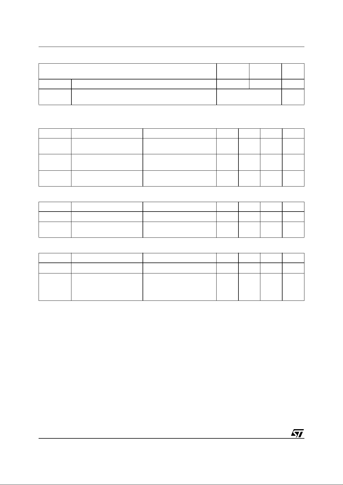
Safe Operating Area for TO-220FPSafe Operating Area for TO-220
3/11
Page 4
STB14NF10 STP14NF10 STP14NF10FP
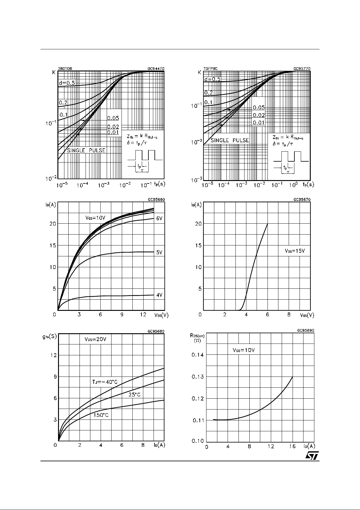
Thermal Impedance Thermal Impedance for TO-220FP
Output Characteristics Transfer Characteristics
Transconductance Static Drain-source On Resistance
4/11
Page 5

STB14NF10 STP14NF10 STP14NF10FP
Gate Charge vs Gate-source Voltage Capacitance Variations
Normalized Gate Threshold Voltage vs Temperature Normalized on Resistance vs Temperature
Source-drain Diode Forward Characteristics Normalized Breakdown Voltage Temperature
5/11
Page 6

STB14NF10 STP14NF10 STP14NF10FP
Fig. 1: Unclamped Inductive Load Test CircuitFig. 1: Unclamped Inductive Load Test Circuit Fig. 2: Unclamped Inductive Waveform
Fig. 3: Switching Times Test Circuits For Resistive
Load
Fig. 5: Test Circuit For Inductive Load Switching
And Diode Recovery Times
Fig. 4: Gate Charge test Circuit
6/11
Page 7

STB14NF10 STP14NF10 STP14NF10FP
D2PAK MECHANICAL DATA
DIM.
A 4.4 4.6 0.173 0.181
A1 2.49 2.69 0.098
A2 0.03 0.23 0.001 0.009
B 0.7 0.93 0.028 0.037
B2 1.14 1.7 0.045 0.067
C 0.45 0.6 0.018 0.024
C2 1.21 1.36 0.048 0.054
D 8.95 9.35 0.352 0.368
D1 8 0.315
E 10 10.4 0.394 0.409
E1 8.5 0.334
G 4.88 5.28 0.192 0.208
L 15 15.85 0.591 0.624
L2 1.27 1.4 0.050 0.055
L3 1.4 1.75 0.055 0.069
M 2.4 3.2 0.094 0.126
R 0.4 0.016
V2 0° 8° 0° 8°
MIN. TYP. MAX. MIN. TYP. TYP.
mm. inch.
0.106
7/11
Page 8

STB14NF10 STP14NF10 STP14NF10FP
E
TO-220 MECHANICAL DATA
DIM.
MIN. TYP. MAX. MIN. TYP. MAX.
A 4.40 4.60 0.173 0.181
C 1.23 1.32 0.048 0.051
D 2.40 2.72 0.094 0.107
D1 1.27 0.050
E 0.49 0.70 0.019 0.027
F 0.61 0.88 0.024 0.034
F1 1.14 1.70 0.044 0.067
F2 1.14 1.70 0.044 0.067
G 4.95 5.15 0.194 0.203
G1 2.4 2.7 0.094 0.106
H2 10.0 10.40 0.393 0.409
L2 16.4 0.645
L4 13.0 14.0 0.511 0.551
L5 2.65 2.95 0.104 0.116
L6 15.25 15.75 0.600 0.620
L7 6.2 6.6 0.244 0.260
L9 3.5 3.93 0.137 0.154
DIA. 3.75 3.85 0.147 0.151
mm inch
A
C
D
D1
L2
F1
L5
Dia.
G1
F
F2
L9
G
H2
L7
L6
L4
P011C
8/11
Page 9

STB14NF10 STP14NF10 STP14NF10FP
TO-220FP MECHANICAL DAT A
DIM.
MIN. TYP. MAX. MIN. TYP. MAX.
A 4.4 4.6 0.173 0.181
B 2.5 2.7 0.098 0.106
D 2.5 2.75 0.098 0.108
E 0.45 0.7 0.017 0.027
F 0.75 1 0.030 0.039
F1 1.15 1.7 0.045 0.067
F2 1.15 1.7 0.045 0.067
G 4.95 5.2 0.195 0.204
G1 2.4 2.7 0.094 0.106
H 10 10.4 0.393 0.409
L2 16 0.630
L3 28.6 30.6 1.126 1.204
L4 9.8 10.6 0.385 0.417
L6 15.9 16.4 0.626 0.645
L7 9 9.3 0.354 0.366
Ø 3 3.2 0.118 0.126
mm inch
A
B
H
E
D
L3
L6
L7
¯
F1
F
G1
G
F2
123
L2
L4
9/11
Page 10

STB14NF10 STP14NF10 STP14NF10FP
D2PAK FOOTPRINT
TAPE AND REEL SHIPMENT (suffix ”T4”)*
TUBE SHIPMENT (no suffix)*
REEL MECHANICAL DATA
DIM.
A 330 12.992
B 1.5 0.059
C 12.8 13.2 0.504 0.520
D 20.2 0.795
G 24.4 26.4 0.960 1.039
N 100 3.937
T 30.4 1.197
mm inch
MIN. MAX. MIN. MAX.
TAPE MECHANICAL DATA
DIM.
A0 10.5 10.7 0.413 0.421
B0 15.7 15.9 0.618 0.626
D 1.5 1.6 0.059 0.063
D1 1.59 1.61 0.062 0.063
E 1.65 1.85 0.065 0.073
F 11.4 11.6 0.449 0.456
K0 4.8 5.0 0.189 0.197
P0 3.9 4.1 0.153 0.161
P1 11.9 12.1 0.468 0.476
P2 1.9 2.1 0075 0.082
R50 1.574
T0.25 0.35 .0.0098 0.0137
W 23.7 24.3 0.933 0.956
mm inch
MIN. MAX. MIN. MAX.
* on sales type
10/11
BASE QTY BULK QTY
1000 1000
Page 11

STB14NF10 STP14NF10 STP14NF10FP
Information furnished is believed to be accurate and reliable. However, STMicroelectronics assumes no responsibility for the consequences
of use of such information nor for any infringement of patents or other rights of third parties which may result from its use. No license is granted
by implic ation or otherwise unde r any patent or patent rights of STMicroelectroni cs. Specifications me ntioned in th i s publication are subj ect
to change without notice. This publication supersedes and replaces all information previously supplied. STMicroelectronics produ ct s are not
authorized for use as crit i cal component s in l i fe support dev i ces or systems without express written approval of STMic roelectronics.
The ST logo is registered trademark of STMicroelectronics
2002 STMi croelectroni cs - All Rights Reserved
All other na m es are the property of their respective owners.
Australi a - Brazil - Cana da - China - Finland - France - Germany - Hong Ko ng - India - Israel - Italy - Japa n - M al aysia - Malta - Morocco -
Singap ore - Spain - Sweden - Switzerl and - United Ki ngdom - United S tates.
STMicroelectronics GROUP OF COMPANIES
http:// www.st.com
11/11
 Loading...