

Page 1
STP14NF06
N-CHANNEL 60V - 0.1Ω - 14A TO-220
STripFET™ POWER MOSFET
TYPE V
DSS
STP14NF10 60 V < 0.12
■ TYPICAL R
■ EXCEPTIONA L dv/d t CAPABILITY
■ LOW GATE CHARGE AT 100 °C
■ APPLICATION ORIENTED
(on) = 0.1Ω
DS
R
DS(on)
I
D
Ω
14 A
CHARACTERIZATION
DESCRIPTION
This Power MOSFET is t he latest development of
STMicroelectronics unique "Single Feature Size™"
strip-based process. The resulting transistor shows
extremely high packing density for low on-resistance, rugged avalanche characteristics and less
critical alignment steps therefore a remarkable
manufacturing reproducibility.
APPLICATIONS
■ DC-DC & DC-AC CONVERTERS
■ MOTOR CONTROL, AUDIO AMPLIFIERS
■ HIGH CURRENT, HIGH SPEED SWITCHING
■ SOLENOID AND RELAY DRIVERS
■ AUTOMOTIVE ENVIRONMENT
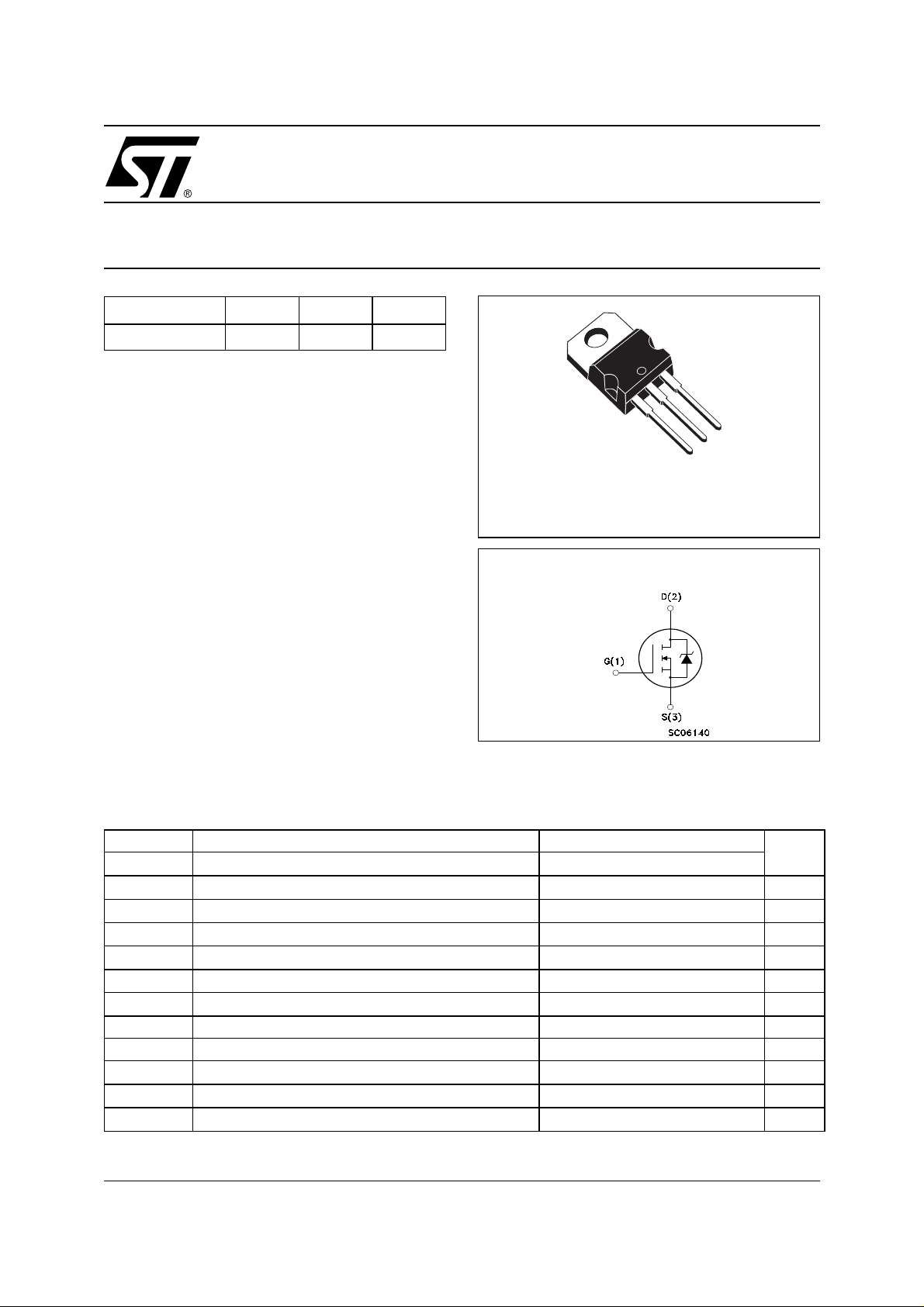
3
2
1
TO-220
INTERNAL SCHEMATIC DIAGRAM
ABSOLUTE MAXIMUM RATINGS
Symbol Parameter Value Unit
V
DS
V
DGR
V
GS
I
D
I
D
I
DM
P
TOT
dv/dt (1) Peak Diode Recovery voltage slope 6 V/ns
E
AS
T
stg
T
j
(●) Pulse width limited by safe operating area
Drain-source Voltage (VGS = 0)
Drain-gate Voltage (RGS = 20 kΩ)
60 V
60 V
Gate- source Voltage ±20 V
Drain Current (continuos) at TC = 25°C
Drain Current (continuos) at TC = 100°C
(●)
Drain Current (pulsed) 56 A
Total Dissipation at TC = 25°C
14 A
10 A
45 W
Derating Factor 0.3 W/°C
(2)
Single Pulse Avalanche Energy 50 mJ
Storage Temperature –65 to 175 °C
Max. Operating Junction Temperature 175 °C
(1) ISD ≤7A, di/dt ≤300A/µs, VDD ≤ V
(2) Starting Tj = 25°C, ID = 114A, VDD = 15V
(BR)DSS
, Tj ≤ T
JMAX.
1/8December 2000
Page 2
STP14NF06
THERMA L D ATA
Rthj-case Thermal Resistance Junction-case Max 3.33 °C/W
Rthj-amb Thermal Resistance Junction-ambient Max 62.5 °C/W
T
l
ELECTRICAL CHARACTERISTICS (TCASE = 25 °C UNLESS OTHERWISE SPECIFIED)
OFF
Symbol Parameter Test Conditions Min. Typ. Max. Unit
V
(BR)DSS
I
DSS
I
GSS
ON
(1)
Symbol Parameter Test Conditions Min. Typ. Max. Unit
V
GS(th)
R
DS(on)
Maximum Lead Temperature For Soldering Purpose 300 °C
Drain-source
ID = 250 µA, VGS = 0 60 V
Breakdown Voltage
Zero Gate Voltage
Drain Current (V
GS
= 0)
Gate-body Leakage
Current (V
DS
= 0)
Gate Threshold Voltage
Static Drain-source On
V
= Max Rating
DS
V
= Max Rating, TC = 125 °C
DS
V
= ±20V ±100 nA
GS
V
= VGS, ID = 250µA
DS
VGS = 10V, ID = 7 A
2V
0.10 0.12
1µA
10 µA
Resistance
Ω
I
D(on)
On State Drain Current VDS > I
D(on)
x R
DS(on)max,
14 A
VGS=10V
DYNAMIC
Symbol Parameter Test Conditions Min. Typ. Max. Unit
(1) Forward Transconductance VDS > I
g
fs
C
iss
C
oss
C
rss
Input Capacitance
Output Capacitance 54 pF
Reverse Transfer
Capacitance
ID= 7 A
V
DS
D(on)
x R
DS(on)max,
= 25V, f = 1 MHz, VGS = 0
7S
361 pF
21 pF
2/8
Page 3
STP14NF06
ELECTRICAL CHARACTERISTICS (CONTINUED)
SWITCHING ON
Symbol Parameter Test Conditions Min. Typ. Max. Unit
V
t
d(on)
Q
Q
Q
t
r
g
gs
gd
Turn-on Delay Time
Rise Time 32 ns
Total Gate Charge
Gate-Source Charge
Gate-Drain Charge
SWITCHING OFF
Symbol Parameter Test Conditions Min. Typ. Max. Unit
t
d(off)
t
f
Turn-off-Delay Time
Fall Time
SOURCE DRAIN DIODE
Symbol Parameter Test Conditions Min. Typ. Max. Unit
I
SD
I
SDM
VSD (2)
t
rr
Q
rr
I
RRM
Note: 1. Pulsed: Pu l se duration = 300 µs, duty cycle 1. 5 % .
2. Pulse width li mited by safe operating area.
Source-drain Current 14 A
(1)
Source-drain Current (pulsed) 56 A
Forward On Voltage
Reverse Recovery Time
Reverse Recovery Charge
Reverse Recovery Current
= 30V, ID = 7 A
DD
R
= 4.7Ω VGS = 10V
G
(see test circuit, Figure 3)
VDD = 48 V, ID = 14 A,
VGS = 10V
VDD = 30 V, ID = 7 A,
RG=4.7Ω, V
GS
= 10V
(see test circuit, Figure 3)
ISD = 14 A, VGS = 0
= 14 A, di/dt = 100A/µs,
I
SD
VDD = 30 V, Tj = 150°C
(see test circuit, Figure 5)
12.5 ns
11.2
15 nC
3.7
3.2
30
9.5
1.3 V
38
61
3.2
nC
nC
ns
ns
ns
nC
A
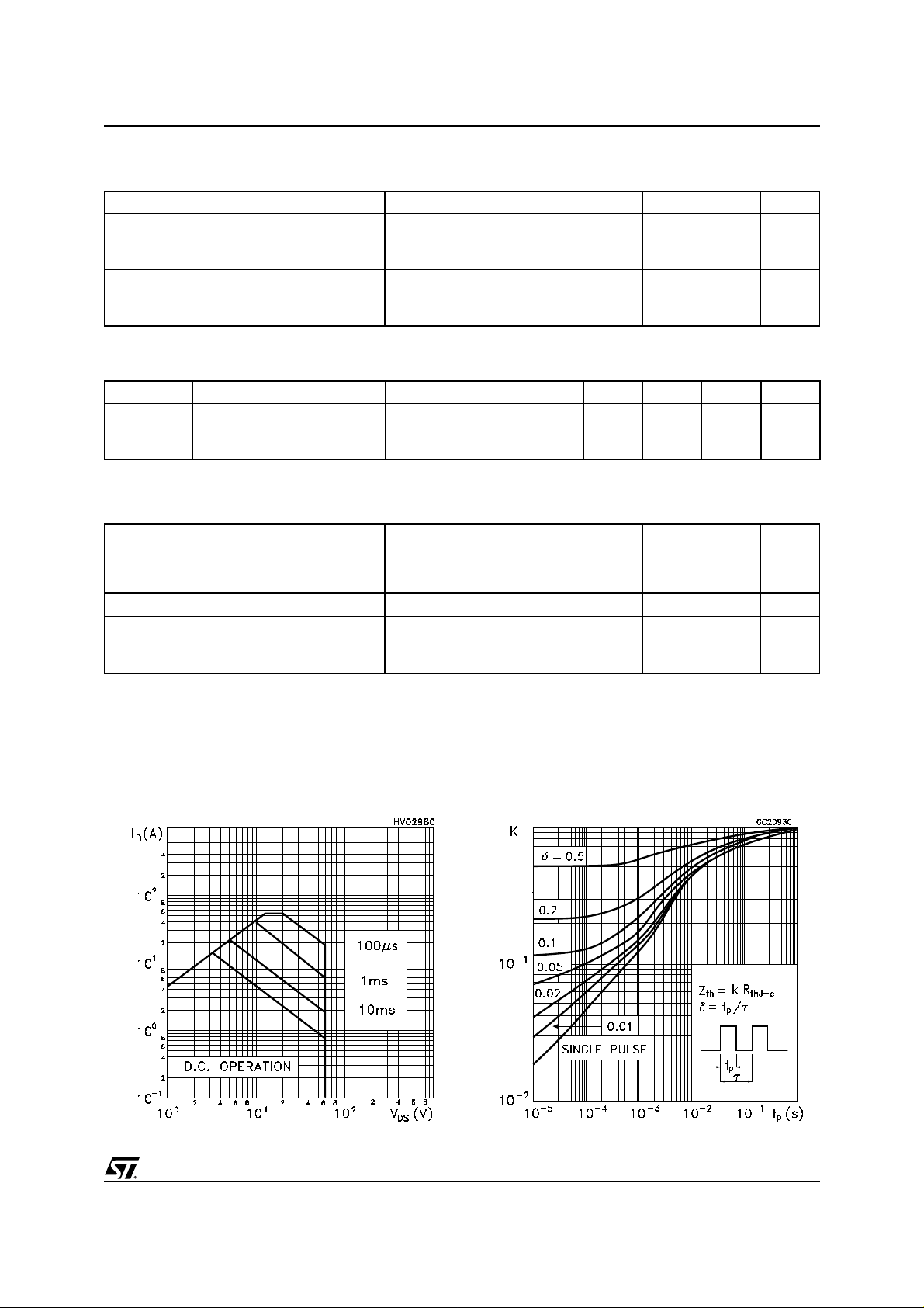
Safe Operating Area Thermal Impedence
3/8
Page 4

STP14NF06
Transfer CharacteristicsOutput Characteristics
Transconductance Static Drain-source On Resistance
Gate Charge vs Gate-source Voltage Capacitance Variation s
4/8
Page 5

STP14NF06
Normalized Gate Thereshold Voltage vs Temp.
Source-drain Diode Forward Characteristics
Normalized On Resistance vs Temperature
5/8
Page 6

STP14NF06
Fig. 2: Unclamped Inductive WaveformFig. 1: Unclamped Inductive Load Test Circuit
Fig. 3: Switching Times Test Circuit For
Resistive Load
Fig. 5: Test Circuit For Inductive Load Switching
And Diode Recovery Times
Fig. 4: Gate Charge test Circuit
6/8
Page 7

E
TO-220 MECHANICAL DATA
STP14NF06
DIM.
A 4.40 4.60 0.173 0.181
C 1.23 1.32 0.048 0.051
D 2.40 2.72 0.094 0.107
D1 1.27 0.050
E 0.49 0.70 0.019 0.027
F 0.61 0.88 0.024 0.034
F1 1.14 1.70 0.044 0.067
F2 1.14 1.70 0.044 0.067
G 4.95 5.15 0.194 0.203
G1 2.4 2.7 0.094 0.106
H2 10.0 10.40 0.393 0.409
L2 16.4 0.645
L4 13.0 14.0 0.511 0.551
L5 2.65 2.95 0.104 0.116
L6 15.25 15.75 0.600 0.620
L7 6.2 6.6 0.244 0.260
L9 3.5 3.93 0.137 0.154
DIA. 3.75 3.85 0.147 0.151
MIN. TYP. MAX. MIN. TYP. MAX.
mm inch
A
C
D
L5
Dia.
L7
D1
L6
L2
L9
F1
G1
F
H2
G
F2
L4
P011C
7/8
Page 8

STP14NF06
8/8
Information furnished is believed to be accurate and reliable. However, STMicroelectronics assumes no responsibility for the consequences
of use of such informa tion n or for an y infring ement of patent s or other rig hts of third part ies which may resu lt from its use . No l i cen se i s
granted by implication or otherwise under any patent or patent rights of STMicroelectronics. Specification mentioned in this publication are
subject to change without notice. This publication supersedes and replaces all information previously supplied. STMicroelectronics products
are not authorized for use as critical compo nents in life support devices or systems without express written approval of STMicroelectronics.
Australia - Brazil - China - Finland - France - Germany - Hong Kong - India - Italy - Japan - Malaysia - Malta - Morocco -
The ST logo is a trademark of STMicroelectronics
© 2000 STMicroelectronics – Printed in Italy – All Rights Reserved
STMicroelectronics GROUP OF COMPANIES
Singapore - Spain - Sweden - Switzerland - United Kingdom - U.S.A.
http://www.st.com
 Loading...