

Page 1

AN5042
Application note
Precise HSE frequency and startup time tuning
for STM32 wireless MCUs
Introduction
This application note describes how to tune the HSE for RF applications using STM32WB
and STM32WL Series microcontrollers (hereinafter referred to as STM32 wireless MCUs).
These products offer a cost-effective and efficient solution by using their internal load
capacitances to control the oscillator accuracy, hence saving the cost of external
capacitances and lowering the crystal constraints.
STM32 wireless MCUs use an external oscillator high-speed clock source as the base for
RF clock generation. HSE accuracy is essential for RF system performance and the
external oscillator is therefore fine-tuned to achieve the highest clock accuracy.
The first part of this application note introduces the crystal oscillator solutions. The second
part introduces and then compares three HSE frequency tuning methods, namely a manual
one, an automatic one and another one based on STM32CubeMonitor-RF (for the
STM32WB Series only). The application of these methods to STM32WB and STM32WL
Nucleo boards is described in the following sections and provided as firmware and script
examples in X-CUBE-CLKTRIM, an STM32Cube Expansion Package.
A specific section of this document is dedicated to a description of how to configure HSE to
make its startup phase reliable and optimized for STM32WB Series microcontrollers.
This application note must be read in conjunction with the reference manuals and
datasheets available at www.st.com.
January 2021 AN5042 Rev 10 1/47
www.st.com
1
Page 2

Contents AN5042
Contents
1 HSE oscillator . . . . . . . . . . . . . . . . . . . . . . . . . . . . . . . . . . . . . . . . . . . . . . 6
1.1 Crystal oscillator . . . . . . . . . . . . . . . . . . . . . . . . . . . . . . . . . . . . . . . . . . . . . 7
1.2 STM32 wireless MCUs architecture . . . . . . . . . . . . . . . . . . . . . . . . . . . . . . 8
1.3 HSE configuration parameters - STM32WB Series . . . . . . . . . . . . . . . . . . 9
1.4 HSE configuration parameters - STM32WL Series . . . . . . . . . . . . . . . . . 10
1.5 Board implementation . . . . . . . . . . . . . . . . . . . . . . . . . . . . . . . . . . . . . . . 10
1.6 Crystal references . . . . . . . . . . . . . . . . . . . . . . . . . . . . . . . . . . . . . . . . . . .11
1.7 Tuning in production . . . . . . . . . . . . . . . . . . . . . . . . . . . . . . . . . . . . . . . . . 12
2 Trimming methods comparison . . . . . . . . . . . . . . . . . . . . . . . . . . . . . . . 13
3 Manual frequency trimming procedure example for
the STM32WB Series . . . . . . . . . . . . . . . . . . . . . . . . . . . . . . . . . . . . . . . . 15
3.1 Procedure description . . . . . . . . . . . . . . . . . . . . . . . . . . . . . . . . . . . . . . . 15
3.2 Implementation . . . . . . . . . . . . . . . . . . . . . . . . . . . . . . . . . . . . . . . . . . . . . 15
3.2.1 Hardware setup . . . . . . . . . . . . . . . . . . . . . . . . . . . . . . . . . . . . . . . . . . . 16
3.2.2 Software implementation . . . . . . . . . . . . . . . . . . . . . . . . . . . . . . . . . . . . 19
3.2.3 Scripts . . . . . . . . . . . . . . . . . . . . . . . . . . . . . . . . . . . . . . . . . . . . . . . . . . 20
4 Manual frequency trimming procedure example for
the STM32WL Series . . . . . . . . . . . . . . . . . . . . . . . . . . . . . . . . . . . . . . . . 21
4.1 Procedure description . . . . . . . . . . . . . . . . . . . . . . . . . . . . . . . . . . . . . . . 21
4.2 Implementation . . . . . . . . . . . . . . . . . . . . . . . . . . . . . . . . . . . . . . . . . . . . . 21
4.2.1 Hardware setup . . . . . . . . . . . . . . . . . . . . . . . . . . . . . . . . . . . . . . . . . . . 22
4.2.2 Software implementation . . . . . . . . . . . . . . . . . . . . . . . . . . . . . . . . . . . . 25
4.2.3 Scripts . . . . . . . . . . . . . . . . . . . . . . . . . . . . . . . . . . . . . . . . . . . . . . . . . . 25
5 Automatic frequency trimming procedure example
for the STM32WB Series . . . . . . . . . . . . . . . . . . . . . . . . . . . . . . . . . . . . . 27
5.1 Procedure description . . . . . . . . . . . . . . . . . . . . . . . . . . . . . . . . . . . . . . . 27
5.2 Implementation . . . . . . . . . . . . . . . . . . . . . . . . . . . . . . . . . . . . . . . . . . . . . 28
5.2.1 Hardware setup . . . . . . . . . . . . . . . . . . . . . . . . . . . . . . . . . . . . . . . . . . . 28
5.2.2 Software implementation . . . . . . . . . . . . . . . . . . . . . . . . . . . . . . . . . . . . 30
5.2.3 Scripts . . . . . . . . . . . . . . . . . . . . . . . . . . . . . . . . . . . . . . . . . . . . . . . . . . 31
2/47 AN5042 Rev 10
Page 3

AN5042 Contents
6 Automatic frequency trimming procedure example
for the STM32WL Series . . . . . . . . . . . . . . . . . . . . . . . . . . . . . . . . . . . . . 33
6.1 Procedure description . . . . . . . . . . . . . . . . . . . . . . . . . . . . . . . . . . . . . . . 33
6.2 Implementation . . . . . . . . . . . . . . . . . . . . . . . . . . . . . . . . . . . . . . . . . . . . . 34
6.2.1 Hardware setup . . . . . . . . . . . . . . . . . . . . . . . . . . . . . . . . . . . . . . . . . . . 34
6.2.2 Software implementation . . . . . . . . . . . . . . . . . . . . . . . . . . . . . . . . . . . . 34
6.2.3 Scripts . . . . . . . . . . . . . . . . . . . . . . . . . . . . . . . . . . . . . . . . . . . . . . . . . . 36
7 STM32CubeMonitor-RF frequency trimming
procedure example for the STM32WB Series . . . . . . . . . . . . . . . . . . . . 37
7.1 Procedure description . . . . . . . . . . . . . . . . . . . . . . . . . . . . . . . . . . . . . . . 37
7.2 Procedure steps . . . . . . . . . . . . . . . . . . . . . . . . . . . . . . . . . . . . . . . . . . . . 37
7.3 Implementation . . . . . . . . . . . . . . . . . . . . . . . . . . . . . . . . . . . . . . . . . . . . . 38
7.3.1 Hardware setup . . . . . . . . . . . . . . . . . . . . . . . . . . . . . . . . . . . . . . . . . . . 38
7.3.2 Software and scripts setup . . . . . . . . . . . . . . . . . . . . . . . . . . . . . . . . . . 38
7.3.3 Scripts . . . . . . . . . . . . . . . . . . . . . . . . . . . . . . . . . . . . . . . . . . . . . . . . . . 39
7.3.4 C code . . . . . . . . . . . . . . . . . . . . . . . . . . . . . . . . . . . . . . . . . . . . . . . . . . 40
8 HSE startup optimization for the STM32WB Series . . . . . . . . . . . . . . . 42
9 Conclusion . . . . . . . . . . . . . . . . . . . . . . . . . . . . . . . . . . . . . . . . . . . . . . . . 44
10 Revision history . . . . . . . . . . . . . . . . . . . . . . . . . . . . . . . . . . . . . . . . . . . 45
AN5042 Rev 10 3/47
3
Page 4

List of tables AN5042
List of tables
Table 1. Carrier accuracy requirement for RF protocols. . . . . . . . . . . . . . . . . . . . . . . . . . . . . . . . . . . 6
Table 2. Oscillator pin numbers for the STM32WB Series . . . . . . . . . . . . . . . . . . . . . . . . . . . . . . . . 10
Table 3. Crystal specifications . . . . . . . . . . . . . . . . . . . . . . . . . . . . . . . . . . . . . . . . . . . . . . . . . . . . . 11
Table 4. Trimming methods . . . . . . . . . . . . . . . . . . . . . . . . . . . . . . . . . . . . . . . . . . . . . . . . . . . . . . . 13
Table 5. Comparison of trimming methods . . . . . . . . . . . . . . . . . . . . . . . . . . . . . . . . . . . . . . . . . . . . 13
Table 6. Document revision history . . . . . . . . . . . . . . . . . . . . . . . . . . . . . . . . . . . . . . . . . . . . . . . . . 45
4/47 AN5042 Rev 10
Page 5

AN5042 List of figures
List of figures
Figure 1. Crystal oscillator principle . . . . . . . . . . . . . . . . . . . . . . . . . . . . . . . . . . . . . . . . . . . . . . . . . . . 7
Figure 2. Crystal oscillator system overview . . . . . . . . . . . . . . . . . . . . . . . . . . . . . . . . . . . . . . . . . . . . 8
Figure 3. UFQFPN48 (USB dongle board) footprint detail. . . . . . . . . . . . . . . . . . . . . . . . . . . . . . . . . 11
Figure 4. Manual calibration overview - STM32WB Series . . . . . . . . . . . . . . . . . . . . . . . . . . . . . . . . 16
Figure 5. OB configuration to boot from SRAM with BOOT0 value driven by PH3 pin . . . . . . . . . . . 17
Figure 6. OB configuration to boot from SRAM with BOOT0 value
driven by option bit nBOOT0 . . . . . . . . . . . . . . . . . . . . . . . . . . . . . . . . . . . . . . . . . . . . . . . 17
Figure 7. Configuration store in OTP bytes . . . . . . . . . . . . . . . . . . . . . . . . . . . . . . . . . . . . . . . . . . . . 20
Figure 8. Manual calibration overview - STM32WL Series . . . . . . . . . . . . . . . . . . . . . . . . . . . . . . . . 22
Figure 9. OB configuration to boot from SRAM with BOOT0 value driven by PH3 pin . . . . . . . . . . . 23
Figure 10. OB configuration to boot from SRAM with BOOT0 value
driven by option bit nBOOT0 . . . . . . . . . . . . . . . . . . . . . . . . . . . . . . . . . . . . . . . . . . . . . . . 23
Figure 11. Automatic calibration overview - STM32WB Series . . . . . . . . . . . . . . . . . . . . . . . . . . . . . . 28
Figure 12. Procedure implementation . . . . . . . . . . . . . . . . . . . . . . . . . . . . . . . . . . . . . . . . . . . . . . . . . 29
Figure 13. Automatic calibration overview - STM32WL Series . . . . . . . . . . . . . . . . . . . . . . . . . . . . . . 34
Figure 14. STM32CubeMonitor-RFcalibration overview - STM32WB Series . . . . . . . . . . . . . . . . . . . 38
AN5042 Rev 10 5/47
5
Page 6
HSE oscillator AN5042
1 HSE oscillator
RF systems require high frequency accuracy to achieve the best performance. Any clock
deviation can cause system malfunctions and/or degrade performance.
Tab l e 1 shows the accuracy requirements for two RF pr
Series microcontrollers. For other protocols and
standards refer to the corresponding
otocols supported by STM32WB
specifications.
Bluetooth
IEEE 802.15.4 / Thread ± 40 ppm
®
In STM32 wireless MCUs, based on Arm
high frequency VCO, which takes
Table 1. Carrier accuracy requirement for RF protocols
RF standard Carrier accuracy
Low Energy ± 50 ppm
®(a)
Cortex® cores, the RF clock is provided by a
as reference a signal created by an embedded oscillator
using an external crystal.
This crystal is the HSE (high-speed external) clock
source of the RF synthesizer and of the
microcontroller. Its nominal frequency can vary, depending on factors such as process
variations, used crystal and PCB design. Since the inaccuracy of the HSE is directly
transferred to the RF clock, it must be fine-tuned by adjusting load capacitance at crystal
terminals.
STM32 wireless MCUs offer an efficient architectu
re with internal load capacitances that
allows the users to fine tune the crystal frequency without extra cost for additional external
capacitances.
The reliability of the startup phase of an
HSE oscillator depends on its actual
implementation (e.g. upon associated crystal, external components, environment). For the
STM32WB Series a method is proposed to adjust its internal operation to optimize and
consolidate this phase. A longer startup improves reliability but increases power
consumption.
Note: AN2867 (Oscillator design guide for
ST microcontrollers), which generally describes HSE
for STM32 product, does not apply to STM32 wireless MCUs due to the RF constraints. This
application note is the correct reference for these products.
a. Arm is a registered trademark of Arm Limited (or its subsidiaries) in the US and/or elsewhere.
6/47 AN5042 Rev 10
Page 7
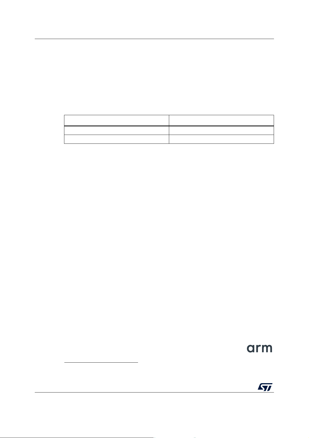
AN5042 HSE oscillator
MSv47132V1
C
L2
C
L1
R
f
Inv
XTAL
C
S
C
L
C
L1CL2
C
L1CL2
+
----------------------------- Cs+=
1.1 Crystal oscillator
Figure 1 shows the crystal oscillator system principle. An oscillator consists of an inverting
amplifier, a feedback resistor (Rf), a crystal (XTAL) and two load capacitors (CL1 and CL2).
C
is the stray capacitance, resulting from the sum of the MCU pin capacitances (OSC_IN
s
and OSC_OUT) and the PCB capacitance: it is a parasitic capacitance.
Figure 1. Crystal oscillator principle
CL load capacitance
The load capacitance is the terminal capacitance of the circuit connected to the crystal
oscillator. This value is determined by the external capacitors C
capacitance of the printed circuit board and connections (C
the crystal manufacturer. For the frequency to be accurate, the oscillator circuit has to show
the same load capacitance to the crystal as the one the crystal was adjusted for.
Frequency stability mainly requires that the load capacitance be constant. The external
trimming capacitors C
and CL2 are used to tune the desired value of CL to reach the value
L1
specified by the crystal manufacturer.
The following equation gives the expression of C
L
Equation 1: Load capacitance
and CL2 and the stray
L1
). The CL value is specified by
s
AN5042 Rev 10 7/47
46
Page 8
HSE oscillator AN5042
MS53500V1
XTAL
OSC_IN
OSC_OUT
Capacitance
Bank IN
Capacitance
Bank OUT
Amplifier
and
Reshaping
Crystal oscillator
STM32WB/WL
HSE_CLK
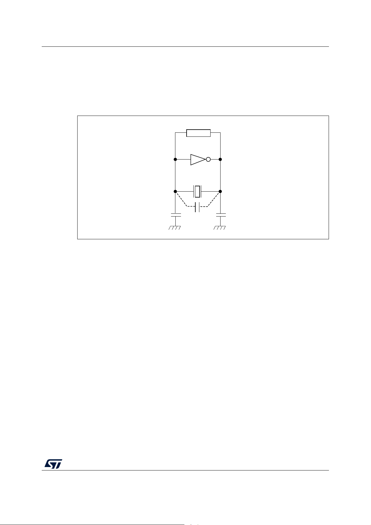
1.2 STM32 wireless MCUs architecture
These MCUs embed an efficient and cost-effective crystal oscillator system with internal
capacitances for trimming. The advantages of the internal mechanism for load capacitance
tuning are twofold:
it reduces the accuracy constraints on the external crystal
it reduces the global BOM (and the footprint) of the PCB.
Figure 2 shows the crystal oscillator system embedded in the STM32 wireless MCUs. The
crystal is the only external component, no extra load capacitances are needed.
Figure 2. Crystal oscillator system overview
The crystal oscillator system consists of two pads (OSC_IN and OSC_OUT) with their
respective capacitance banks, and the amplifier stage.
For STM32WB Series, the capacitance value is the same for both the IN and the OUT
banks. This value, alongside with the oscillator gain and sense (the parameters that make
possible the optimization of the start-up phase), is driven by a register and controls the
system behavior. These parameters are explained in
For STM32WL Series, the capacitance values for the IN and the OUT banks are
independent. These two values are driven by two sub-GHz radio registers and control the
system behavior. These parameters are explained in
8/47 AN5042 Rev 10
Section 1.3.
Section 1.4.
Page 9
AN5042 HSE oscillator
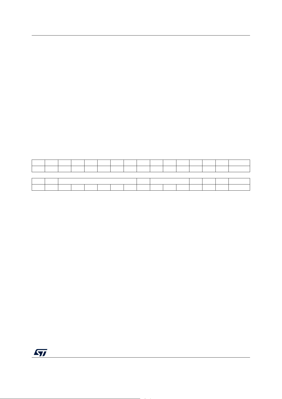
1.3 HSE configuration parameters - STM32WB Series
Three parameters can be set to control the oscillator module. They are accessible
in the RCC_HSECR register described below.
RCC_HSECR
Address 0x09C
Reset 0x0000 0030
Access This register is protected to avoid on-the-fly modification.
A key (0xCAFECAFE) must be written at the register address to unlock it
before any single write access, it is then locked again.
The HSE clock must be switched off during register access procedure to avoid
unpredictable behavior. Note that HSE must not be used as CPU clock source
during this step.
In this document the default MSI clock is used as system clock source after
startup from Reset.
31 30 29 28 27 26 25 24 23 22 21 20 19 18 17 16
Res. Res. Res. Res. Res. Res. Res. Res. Res. Res. Res. Res. Res. Res. Res. Res.
15 14 13 12 11 10 9 8 7 6 5 4 3 2 1 0
Res. Res. HSETUNE[5:0] Res. HSEGMC[2:0] HSES Res. Res. UNLOCKED
rw rw rw rw rw rw rw rw rw rw rw
Load capacitance: HSETUNE[5:0]
This is the parameter responsible for the clock accuracy. It selects the capacitance value
added on both input and output pads. The adjustable range is set to have a global load
capacitance comprised between 12 and 16 pf. The minimum (0x00) and maximum (0x3F)
values correspond, respectively, to the smallest and to the largest load capacitance.
Default value is 0x00 (minimum load capacitance).
Current control: HSEGMC[2:0]
This parameter (referred to as Gm or Gm_crit_max in the documentation of other STM32
products for which it has a fixed value) is the maximum critical crystal transconductance of
the oscillator. It controls the startup performance of the system. A low value decreases the
power consumption, while a high value improves the startup time.
The minimum value (0b000) corresponds to Gm = 0.18 mA/V, the maximum value (0b111)
to Gm = 2.84 mA/V. Default value is 0x3 (Gm = 1.13 mA/V).
HSES sense amplifier threshold
This parameter controls an internal comparison threshold for the oscillator startup. When
this bit is set (1), the startup time is reduced (from around 15 µs) but the current
consumption is higher.
Default value is 0x0 (1/2 ratio).
AN5042 Rev 10 9/47
46
Page 10
HSE oscillator AN5042
1.4 HSE configuration parameters - STM32WL Series
For the STM32WL Series two parameters can be set to control the oscillator module. They
are accessible in the SUBGHZ_HSEINTRIMR and the SUBGHZ_HSEOUTTRIMR sub-GHz
radio registers, which contain the capacitance value of the IN and OUT banks, respectively.
The associated value is represented by their six lower bits (the remaining bits of these
registers must be kept at their reset values).
For both registers:
0x00 corresponds to the minimum capacitance (~11.3 pF)
0x2F corresponds to the maximum capacitance (~33.4 pF)
the values must not exceed 0x2F and the trimming step is ~0.47 pF
the reset value is 0x12, which corresponds to ~20.3 pF.
As mentioned earlier, SUBGHZ_HSEINTRIMR and SUBGHZ_HSEOUTTRIMR are part of
the sub-GHz radio and not of the system CPU. To modify their values the user code needs
to communicate with the sub-GHz radio via its SPI interface. The addresses of these
registers, considering this SPI interface, are 0x911 for SUBGHZ_HSEINTRIMR and 0x912
for SUBGHZ_HSEOUTTRIMR.
1.5 Board implementation
Oscillator pads are available on different pins (named OSC_IN and OSC_OUT), depending
upon the package.
Tab l e 2 shows the pin numbers for four different packages used in
Nucleo and USB dongle boards for the STM32WB Series.
Table 2. Oscillator pin numbers for the STM32WB Series
Package OSC_IN OSC_OUT
UFQFPN48 25 24
VFQFPN68 35 34
WLCSP100 J1 J2
BGA129 M13 N13
The crystal is plugged directly onto the pads, with no extra capacitance, and as close as
possible to the device to minimize parasitic capacitance.
Figure 3 shows a typical UFQFPN48 footprint for the STM32WB Series.
10/47 AN5042 Rev 10
Page 11
AN5042 HSE oscillator
MS47142V1
OSC_IN
OSC_OUT
Crystal_pins
GND
Figure 3. UFQFPN48 (USB dongle board) footprint detail
The PCB layout for the STM32WB and STM32WL Series reference designs are detailed,
respectively, in AN5165 “Development of RF hardware using STM32WB microcontrollers”
and AN5407 “Optimized RF board layout for STM32WL Series”, both available on
www.st.com.
1.6 Crystal references
Tab l e 3 shows the specification of the crystals used to validate the reference designs.
Series NDK crystal Parameter Value
STM32WB
STM32WL
NX2016SA 32 MHz
EXS00A-CS06654
NX2016SA 32 MHz
EXS00A-CS06465
Table 3. Crystal specifications
Load capacitance 8 pF
Frequency tolerance (25 ± 3 °C) ± 10 × 10
Frequency vs. temperature
(with reference to +25 °C)
Load capacitance 10 pF
Frequency tolerance ± 10 ppm at 25 °C
Frequency vs. temperature
−6
± 25 × 10
−6
± 10 ppm (-25 to +70 °C)
± 30 ppm (-40 to +85 °C)
AN5042 Rev 10 11/47
46
Page 12

HSE oscillator AN5042
It is possible to use other crystals, as long as they respect the carrier accuracy requirements
(see
Tabl e 1). More precisely, the sum of the maximum values for the following parameter
specifications of the chosen crystal must be below the carrier accuracy requirements:
frequency tolerance
frequency versus temperature characteristics (for the temperature in which the crystal
must be used)
aging (for the duration during which the crystal must be used).
Note: Such data can be named differently or absent in the crystal documentation.
The previous verification is reliable if the PCB based on the chosen crystal is designed with
the requirements mentioned in
methods described in the next sections of this document.
Note that the accuracy of the capacitance bank used for the HSE trimming can vary from a
product to another. If the carrier accuracy verification is needed for the whole production
chain refer to
Section 1.7.
Section 1.5 and fine-tuned with one of the HSE trimming
1.7 Tuning in production
With mass production in perspective, it is important to know if the trimming parameters
defined for a test PCB will have the same efficiency when applied to all the PCBs to be
produced.
To have a faster and more efficient production chain, it is not mandatory to operate the
trimming process on each PCB.
Data gathered during the production of the STM32WB Nucleo boards have shown some
variations of the HSE frequency for a fixed HSETUNE value (HSETUNE accuracy).
Besides, the typical HSETUNE granularity is 1 ppm (see XOTUNE granularity in STM32WB
datasheets). To compensate for these variations, the following trimming method is
suggested for production:
1. tune some PCBs (not more than a few dozens) to get a significant span of HSETUNE
values
2. calculate the median of the found values, and use the result to trim all other PCBs
3. the interval between the median and the maximum/minimum of the found values
corresponds to the HSETUNE accuracy for the tuned design.
Moreover, after having followed this process, a potential frequency deviation due to the
HSETUNE accuracy (point
accuracy verification calculation presented in Section 1.6.
A similar method can be used for STM32WL Series. The number of test boards must be
larger because of the two trimming parameters for these products.
3) has to be taken into account and added to the carrier
12/47 AN5042 Rev 10
Page 13

AN5042 Trimming methods comparison
2 Trimming methods comparison
The three trimming methods described in this document are detailed in Tabl e 4, and
compared in Tabl e 5.
Method Description
Manual
Automatic
STM32CubeMonitor-RF
(1)
Table 4. Trimming methods
A precision frequency meter is used to measure the HSE frequency
output on one of the STM32 pins. Then, the user tunes the HSE
frequency with the buttons of a Nucleo board. A button is dedicated to
the saving of the tuning parameters in the STM32 non-volatile memory.
One STM32 timer is clocked with a precision external clock source
provided by the user via one of the STM32 pins. This reference clock
allows the user to measure the internal STM32 system HSE frequency.
Then, the STM32 can compare the frequency measured with the one
expected, to test and determine the best tuning parameters. Finally, the
STM32 saves these parameters in its non-volatile memory.
A precision frequency meter is used to measure the HSE frequency
output on one of the STM32 pins. Then, the user tunes the HSE
frequency with a script to run in STM32CubeMonitor-RF. The user has
to change the tuning parameter values in the script to test them. When
the correct values are found, another script saves them in the STM32
non-volatile memory.
1. Compatible with STM32WB Series only.
Table 5. Comparison of trimming methods
Method Advantages Disadvantages
Manual
Runs in SRAM (user program in
Flash memory is not affected).
Needs the use of buttons and a
frequency meter for each product.
Runs in SRAM (user program in
Automatic
Flash memory is not affected).
The user needs to set up a
reference clock only once to trim as
Method based on a more complex
principle.
many devices as wanted.
BLE stack and transparent mode
FW must be flashed in the device.
Requires several actions from the
user for each product (modifying
and running the script, use of a
STM32CubeMonitor-RF
Convenient for users familiar with
(1)
STM32CubeMonitor-RF, willing to
achieve the maximum functionality.
frequency meter).
1. Compatible with STM32WB Series only.
Note: The proposed methods require the use of a pin (MCO) to output the HSE signal for the
frequency measurement. If no MCO pin is available for this purpose, AN5378 (available on
www.st.com) describes another technique: instead of measuring the frequency on the MCO
pin, it proposes to do the measurement on a tone frequency emitted by the STM32WB
radio. However, while this tone is emitted, HSE cannot be trimmed because it is used by the
AN5042 Rev 10 13/47
46
Page 14

Trimming methods comparison AN5042
radio (actually this is more a verification than a real trimming method like those exposed in
this document).
14/47 AN5042 Rev 10
Page 15

AN5042 Manual frequency trimming procedure example for the STM32WB Series
3 Manual frequency trimming procedure example for
the STM32WB Series
The firmware and scripts associated to this document are available as an STM32Cube
Expansion Package
(X-CUBE-CLKTRIM_vx.y\Projects\P-NUCLEO-WB55.Nucleo\RCC_HSE_Calib).
3.1 Procedure description
The procedure consists in measuring the HSE clock generated inside the device from the
external crystal. This clock is output on pin PA8 and is measured by a precision frequency
meter.
Note: An external reference is mandatory since no such accurate one is integrated in the device.
A step-by-step tuning of the load capacitance is performed to reach the best accuracy of the
HSE clock. The load capacitance value is then stored inside a non-volatile location of the
device, either a dedicated area of the user Flash memory or in the One-Time-Programming
area.
Flash memory or OTP programming is done with a double-word granularity (64 bits). To
save OTP bytes (1
be appended to a 64-bit wide structure with other personalization data (such as the
Bluetooth
®
device address, the MAC short address, the product specific code, the key).
K in the STM32WB Series), the load capacitance value on six bits can
This procedure can be done several times, only the latest setup is active.
Once the procedure is completed, the active load capacitance value can be retrieved at
startup (in the clock configuration function) and the HSE configuration register set
accordingly.
3.2 Implementation
The procedure is executed in SRAM, so it can be run on an already programmed device
without modifying the Flash memory content.
AN5042 Rev 10 15/47
46
Page 16

Manual frequency trimming procedure example for the STM32WB Series AN5042
3.2.1 Hardware setup
Figure 4 shows the manual calibration procedure for a STM32WB Series Nucleo-68 board.
Figure 4. Manual calibration overview - STM32WB Series
A precision frequency meter (better than 0.1 ppm) must be connected to pin PA8/MCO and
must be set to detect a 32
Note: Standard oscilloscopes are not sufficiently accurate for this kind of measurement.
MHz 3.3 V square wave peak to peak signal.
Boot from SRAM
Boot selection can be done through the BOOT0 pin and nBOOT1 bit in the User options
(FLASH_OPTR).
The boot from SRAM configuration is set by both Boot0 = 1 and nBoot1 = 0 conditions,
nBoot1 is set only by option bit FLASH_OPTR[23].
Boot0 can be selected
through value of pin PH3 at startup if option bit nSWBOOT0 = 1
(FLASH_OPTR[26] = 1), see the option byte panel in Figure 5
through option bit value nBOOT0 if option bit nSWBOOT0 = 0 (FLASH_OPTR[26] = 0),
see the option byte panel in Figure 6
Option bits can be selected through STM32CubeProgrammer.
16/47 AN5042 Rev 10
Page 17

AN5042 Manual frequency trimming procedure example for the STM32WB Series
Figure 5. OB configuration to boot from SRAM with BOOT0 value driven by PH3 pin
Figure 6. OB configuration to boot from SRAM with BOOT0 value
driven by option bit nBOOT0
AN5042 Rev 10 17/47
46
Page 18

Manual frequency trimming procedure example for the STM32WB Series AN5042
Clock output
HSE clock is output on the pin PA8 (MCO), which is available on connectors CN9/D6 and
CN10/25. PA8 configuration is performed in the firmware. Frequency meter probe is
connected to one of these connectors and ground can be taken from connector CN11 or
CN12. According to the type of frequency meter used, AC coupling instead of DC may be
needed.
The next sequence is required to output the HSE on the MCO pin.
1. Turn on the HSE oscillator:
a) Set clock control register RCC_CR[16] = 1
2. Configure PA8 pin to Clock output function
a) Select GPIO alternate function to MCO (= 0x0)
b) Select GPIO speed to Very high frequency (= 0x3)
3. Select HSE as output clock with no division factor:
a) Clock configuration register RCC_CFGR[30:24] = 0b000_0100
Load capacitance setting
The RCC_HSECR[13:8] register drives the load capacitance.
The proposed procedure uses the three push-button available on the Nucleo68 board to
modify the register value:
Pushing SW1 button increases this value by 1.
Pushing SW2 button saves it in the non-volatile memory.
Pushing SW3 button decreases it by 1.
– Initial value is set to 0 after reset, it cannot be increased above 0x3F (maximum
load capacitance) and cannot be decreased below 0x0 (minimum load
capacitance). After each action, the frequency has to be measured.
The next sequence is required for each tested value:
1. Disable the HSE clock:
– Clock control register RCC_CR[16] = 0
2. Unlock RCC_HSECR register:
– WRITE_REG(RCC_HSECR, 0xCAFECAFE);
3. Write the six bits of load capacitance in RCC_HSECR[13:8]
4. Turn on the HSE oscillator:
– Clock control register RCC_CR[16] = 1
Other fields of the register remain unchanged in this procedure and keep their initial value:
HSE current control (HSEGMC = RCC_HSECR[6:4]) is set to 0x3 → current max limit
1.13 mA / V.
HSE sense amplifier threshold (HSES = RCC_HSECR[3]) is set to 0 → HSE bias
current factor 1/2
18/47 AN5042 Rev 10
Page 19

AN5042 Manual frequency trimming procedure example for the STM32WB Series
3.2.2 Software implementation
Project configurations
Two project configurations are available in the package, one for the calibration procedure
(STM32WBxx_Nucleo_Set_Calibration), another one to test the stored value
(STM32WBxx_Nucleo_Test_Calibration). This last configuration is given as an
implementation example of the HSE clock initialization in RF applications.
The firmware is built on the STM32WB HAL drivers.
1. STM32WBxx_Nucleo_Set_Calibration: the device is programmed to:
– Send the HSE clock on the PA8 pin.
– Modify and set the load capacitance value when push-buttons SW1 and SW3 are
actioned.
– Store the load capacitance value together with the 48 bits of additional data
(Bluetooth device address) in the OTP or the selected Flash area when SW2
button is pushed.
2. STM32WBxx_Nucleo_Test_Calibration: configuration to test the actual HSE settings:
– Configure the HSE clock and output it on PA8 pin.
– Fetch the load capacitance value from the OTP/Flash memory area.
– Program RCC_HSECR register accordingly.
Storage in OTP (one-time-programmable) bytes
Load capacitance value is included in a 64-bit structure. Each OTP structure type is
indicated by its index (one byte). The index used for the structure in this application note
is
0. Six bytes remain to store additional data like MAC, Bluetooth device address or crypto
key.
typedef __packed struct
{
uint8_t additional _data[6]; /* 48 bits */
uint8_t hse_tuning; /* Load capacitance value */
uint8_t index; /* structure index ==0x00*/
} OTP_BT_t;
AN5042 Rev 10 19/47
46
Page 20

Manual frequency trimming procedure example for the STM32WB Series AN5042
MSv47146V1
OTP_data
Idx = n
OTP_data
Idx = m
0x1FFF7000
0x1FFF7008 0x1FFF7010
0x1FFF7018
0x1FFF7020
Previous calibration
obsolete
Current OTP_data
for HSE
Next free OTP
double-word
0xFFFFFFFF_FFFFFFFF
OTP_data
Idx = 0
OTP_data
Idx = 0
Even if the configuration phase is not supposed to be repeated, there may be some case
when it must be overwritten. When using OTP bytes, the current configuration cannot be
removed, hence the new one is placed at the next free double-word slot (see
Figure 7).
Figure 7. Configuration store in OTP bytes
When the calibration phase has been done, the application initialization phase must retrieve
the load capacitance (and other additional data) from this OTP area. The value retained is
then the last one with the right index.
3.2.3 Scripts
Two batch scripts are provided to run each firmware configuration:
1. STM32WBxx_Nucleo_Set_HSE_Calibration_OTP.bat
2. STM32WBxx_Nucleo_Test_HSE_Calibration_OTP.bat
These scripts call the STM32CubeProgrammer in command-line mode, and the path to the
tool must be set accordingly: SET CLI="C:\Program Files
(x86)\STMicroelectronics\STM32Cube\STM32CubeProgrammer\bin\STM32_Programmer_
CLI.exe.
The binary or hex file of the configuration must be set also (example for Set_Calibration)
1. For Keil®:
SET HEXFILE="STM32WBxx_Nucleo\STM32WBxx_Nucleo_Set_Calibration.hex"
2. For IAR™:
SET HEXFILE="STM32WBxx_Nucleo_Set_Calibration\Exe\
STM32WBxx_Nucleo_Set_Calibration.hex"
3. For STM32CubeIDE:
SET HEXFILE="STM32WBxx_Nucleo_Set_Calibration\Debug\
STM32WBxx_Nucleo_Set_Calibration.hex"
The 48 bits of additional data (last parameter) are transmitted to the device through these
scripts. They are stored inside the SRAM and read by the FW.
%CLI% -c port=swd -w32 0x2002FFF0 0x33445566
%CLI% -c port=swd -w32 0x2002FFF4 0x00001122
20/47 AN5042 Rev 10
Page 21

AN5042 Manual frequency trimming procedure example for the STM32WL Series
4 Manual frequency trimming procedure example for
the STM32WL Series
The firmware associated to this application note is available as an STM32Cube Expansion
Package
(X-CUBE-CLKTRIM_vx.y\Projects\Nucleo-WL55JC\RCC_HSE_Calib_SingleCore).
Note: The trimmed NUCLEO-WL55JC board needs to be configured to use the on-board crystal
as HSE instead of the TCXO (which adjusts its frequency autonomously, according to the
temperature). For details refer to UM2592, available on www.st.com.
4.1 Procedure description
The procedure consists in measuring the HSE clock generated inside the device from the
external crystal. This clock is output on pin PA8 and is measured by a precision frequency
meter.
Note: An external reference is mandatory since no such accurate internal one exists in the device.
A step-by-step tuning of the load capacitance is performed to reach the best accuracy of the
HSE clock. The IN and OUT banks load capacitance values are then stored in a non-volatile
location of the device, either a dedicated area of the user Flash memory or in the OTP
programming area.
Flash memory or OTP programming is done with a double-word granularity (64 bits). To
save OTP bytes (1 K in the STM32WL Series), the IN and OUT load capacitance values,
each one on six bits, can be appended to a 64-bit wide structure with other personalization
data (such as device address, product specific code, key).
This procedure can be done several times, only the last setup is active.
Once the procedure is completed, the active load capacitance value can be retrieved at
startup (in the clock configuration function) and the HSE configuration register set
accordingly.
4.2 Implementation
The procedure runs in SRAM, so it can be executed on an already programmed device
without modifying the Flash memory content.
AN5042 Rev 10 21/47
46
Page 22

Manual frequency trimming procedure example for the STM32WL Series AN5042
4.2.1 Hardware setup
Figure 8 shows the manual calibration procedure for a STM32WL Series Nucleo board.
Figure 8. Manual calibration overview - STM32WL Series
A precision frequency meter (better than 0.1 ppm) must be connected to pin PA8/MCO and
set to detect a 32 MHz square wave 3.3 V peak to peak signal.
Note: Standard oscilloscopes are not enough accurate for this kind of measurement.
Boot from SRAM
Boot selection can be done through the BOOT0 pin and nBOOT1 bit in the user options
(FLASH_OPTR).
The boot from SRAM configuration is set by both BOOT0 = 1 and nBOOT1 = 0 conditions,
nBOOT1 is set only by option bit FLASH_OPTR[23].
BOOT0 can be selected
through value of pin PH3 at startup if option bit nSWBOOT0 = 1
(FLASH_OPTR[26] = 1), see the option byte panel in Figure 9
through option bit value nBOOT0 if option bit nSWBOOT0 = 0 (FLASH_OPTR[26] = 0),
see the option byte panel in Figure 10
Option bits can be selected through STM32CubeProgrammer.
22/47 AN5042 Rev 10
Page 23

AN5042 Manual frequency trimming procedure example for the STM32WL Series
Figure 9. OB configuration to boot from SRAM with BOOT0 value driven by PH3 pin
Figure 10. OB configuration to boot from SRAM with BOOT0 value
driven by option bit nBOOT0
AN5042 Rev 10 23/47
46
Page 24

Manual frequency trimming procedure example for the STM32WL Series AN5042
Clock output
HSE clock is output on pin PA8 (MCO), available on connectors CN10/16. PA8 configuration
is performed by the firmware. Frequency meter probe is connected to this connector and
ground can be taken from connector CN3 or CN4. According to the type of frequency meter
used, it can be needed to use AC coupling instead of DC.
The next sequence is required to output the HSE on the MCO pin.
1. Turn on the HSE oscillator:
a) Set clock control register RCC_CR[16]=1
2. Configure PA8 pin to clock output function:
a) Select GPIO alternate function to MCO (= 0x0)
b) Select GPIO speed to Very high frequency (= 0x3)
3. Select HSE as output clock with no division factor:
a) Clock configuration register RCC_CFGR[30:24] = 0b000_0100
Load capacitance setting
The SUBGHZ_HSEINTRIMR[5:0] bits set the capacitance for bank IN.
The SUBGHZ_HSEOUTTRIMR[5:0] bits set the capacitance for bank OUT.
The proposed procedure uses the three push-buttons available on the Nucleo board to
modify the registers value:
After startup, each push of SW1 or SW3 respectively increases the value of
SUBGHZ_HSEINTRIMR and SUBGHZ_HSEOUTTRIMR by 1.
One short push on SW2 changes the variations direction. For example if we push one
time SW2 after startup, then each SW1 / SW3 push respectively decreases the value of
SUBGHZ_HSEINTRIMR / SUBGHZ_HSEOUTTRIMR by 1. Another SW2 push sets
back an increasing variations direction, another one sets back a decreasing variations
direction, and so on.
Pushing SW2 for two seconds (the three Nucleo LEDs blink at the same time when the
push has been taken into account) stores the parameters in memory (OTP or Flash
memory according to constants defined by the user).
For these two registers the initial value is set to 0x12 (20.3 pF) after reset. It cannot be
increased above 0x2F (maximum load capacitance 33.4 pF), and cannot be decreased
below 0x0 (minimum load capacitance 11.3 pF). After each action, the frequency must be
measured.
The next sequence is required for each tested value:
1. Enter the sub-GHz radio in standby with HSE32 mode:
sends the command code 0x80 to the sub-GHz radio SPI interface with no parameters
(set the parameter to 0 by default).
2. Write the six bits of load capacitance in SUBGHZ_HSEINTRIMR[5:0] or
SUBGHZ_HSEOUTTRIMR[5:0]:
sends the command code 0x0D (write register command) to the sub-GHz radio SPI
interface followed by the register address (0x0911 for SUBGHZ_HSEINTRIMR and
0x0912 for SUBGHZ_HSEOUTTRIMR) and the value they have to take.
3. Enter the sub-GHz radio in FS (frequency synthesis) mode (to exit standby mode):
sends the command code 0xC1 to the sub-GHz radio SPI interface with no parameters
(set the parameter to 0 by default).
24/47 AN5042 Rev 10
Page 25

AN5042 Manual frequency trimming procedure example for the STM32WL Series
4.2.2 Software implementation
Project configurations
Two project configurations are available in the package, one for the calibration procedure
(determination called RCC_HSE_Calib_SingleCore) and another to test the stored value
(called RCC_HSE_Calib_SingleCore_Test). The latter configuration is given as an
implementation example of the HSE clock initialization in RF applications.
The firmware is built on the STM32WL HAL drivers.
1. RCC_HSE_Calib_SingleCore: the device is programmed to:
a) Send the HSE clock on the PA8 pin.
b) Modify and set the IN and OUT load capacitance values when push-buttons SW1
and SW3 are actioned (short push on SW2 changes the variations direction).
c) Store the load capacitance value together with the 40 bits of additional data
(Bluetooth device address) in the OTP or the selected Flash area when SW2 is
pushed for two seconds.
2. RCC_HSE_Calib_SingleCore_Test, a configuration to test the saved HSE settings:
a) Configure the HSE clock and output it on PA8 pin.
b) Fetch the IN and OUT load capacitance values from the OTP/Flash area.
c) Program SUBGHZ_HSEINTRIMR and SUBGHZ_HSEOUTTRIMR registers
accordingly.
Storage in OTP bytes
Load capacitance values are included in a 64-bit structure. Each OTP structure type is
indicated by its index (one byte). The index used for the structure in this application note is
0. Five bytes remain to store additional data like device address or crypto key.
typedef __packed struct
{
uint8_t additional _data[5]; /* 48 bits */
uint8_t hse_tuning_in; /* IN bank load capacitance value */
uint8_t hse_tuning_out; /* OUT bank load capacitance value */
uint8_t index; /* structure index ==0x00*/
} OTP_BT_t
Even if the configuration phase is not supposed to be repeated, there may be some case
where it should be overwritten. When using OTP bytes, the current configuration cannot be
removed, so the new one is placed at the next free double-word slot (see
When the calibration phase has been done, the application initialization phase must retrieve
the IN and OUT load capacitances (and other additional data) from this OTP area. The
values retained are the last ones with the right index.
4.2.3 Scripts
Two batch scripts are provided to run each firmware configuration:
RCC_HSE_Calib_SingleCore_OTP.bat
RCC_HSE_Calib_SingleCore_Test_OTP.bat
Figure 7).
AN5042 Rev 10 25/47
46
Page 26

Manual frequency trimming procedure example for the STM32WL Series AN5042
These scripts call the STM32CubeProgrammer command-line interface, and the path to the
tool must be set accordingly:
SET CLI="C:\Program Files (x86)
\STMicroelectronics\STM32Cube\STM32CubeProgrammer\bin\STM32_Programmer_CLI
.exe"
The binary or hex file of the configuration must be set also
For IAR™:
SET BINFILE="RCC_HSE_Calib_SingleCore\Exe\RCC_HSE_Calib_SingleCore.bin"
For Keil®:
SET HEXFILE="RCC_HSE_Calib_SingleCore\Exe\RCC_HSE_Calib_SingleCore.hex"
The 40 bits of additional data (last parameter) are transmitted to the device through these
scripts. They are stored inside the SRAM and read by the firmware.
STM32_Programmer_CLI.exe -c port=swd -w32 0x20006FF0 0x22334455
STM32_Programmer_CLI.exe -c port=swd -w32 0x20006FF4 0x00000011
26/47 AN5042 Rev 10
Page 27

AN5042 Automatic frequency trimming procedure example for the STM32WB Series
5 Automatic frequency trimming procedure example
for the STM32WB Series
The firmware and scripts associated to this document are available as an STM32Cube
Expansion Package
(X-CUBE-CLKTRIM_vx.y\Projects\P-NUCLEO-WB55.Nucleo\RCC_HSE_AutoCalib).
5.1 Procedure description
The procedure consists in measuring the HSE clock generated inside the device from the
external crystal. The measure is done internally to the STM32 system and is based on an
accurate external 16 MHz clock reference provided by the user on PA9.
Note: An external reference is mandatory since no such accurate one is integrated in the device.
An automatic tuning of the load capacitance is performed by a specific STM32 application to
reach the best accuracy of the HSE clock. The load capacitance value found is then stored
in a non-volatile location of the device, in a dedicated area of the user Flash memory or of
the OTP.
Flash memory or OTP programming is done with a double-word granularity (64 bits). To
save OTP bytes (1 K in the STM32WB Series), the load capacitance value on six bits can be
appended to a 64-bit wide structure with other personalization data (such as the Bluetooth
device address, the MAC short address, the product specific code, the key).
This procedure can be done several times, only the latest setup is active.
Once the procedure is completed, the active load capacitance value can be retrieved at
startup (in the clock configuration function) and the HSE configuration register set
accordingly.
AN5042 Rev 10 27/47
46
Page 28

Automatic frequency trimming procedure example for the STM32WB Series AN5042
MS53505V2
PA5/TIM2_ETR
16 MHz precision
reference clock source
PA9/TIM1_CH2
BOOT0 to 3.3V
PA8/MCO
5.2 Implementation
5.2.1 Hardware setup
Figure 11 shows the automatic calibration procedure for a STM32WB Series
Nucleo-68 board.
Figure 11. Automatic calibration overview - STM32WB Series
Note: A standard signal generator does not give enough accuracy for this application.
Note: OFF time is needed to temporize and wait for HSE stabilization when several HSE
A precision clock generator (better than 0.1 ppm) must be connected to pin PA9/TIM1_CH2,
and set to generate a 16 MHz, 3.3 V
as to boot from SRAM refer to
Section 3.2.1: Hardware setup.
square wave. To see how to configure the board so
PP
Hardware connections principle
Two timers (TIMER1 and TIMER2) are used by the MCU to exploit the external reference
clock and thus to measure and tune the HSE frequency.
TIMER1 is clocked by the 16 MHz precision external reference clock and generate a PWM
signal low during an OFF time (fixed to 16 ms) and high during a REF time (100 or 1000
depending on the stage of the calibration procedure).
This PWM signal is used to enable TIMER2 counter when high.
TIMER2 is clocked by HSE/2 output on MCO pin.
Then, after one PWM signal period, TIMER2 counter corresponds to the number of HSE/2
periods elapsed during REF time.
This value can be compared to the expected value to adjust the load capacitance
conditioning HSE frequency.
measurements are done in sequence.
ms,
28/47 AN5042 Rev 10
Page 29

AN5042 Automatic frequency trimming procedure example for the STM32WB Series
MS5308V1
TIM1
TRGO
TIM2
ITR0
PA9
PA5
PA8
HSE/2 = 16 MHz
(frequency to tune)
TIM1_CH2/TI2
ETR
MCO
STM32
16 MHz precision
reference clock source
Figure 12 illustrates the connections between the elements involved in the procedure.
Figure 12. Procedure implementation
TIMER1 configuration
TIM1 is configured to be clocked by a 16 MHz external signal provided on PA9. PA9 is
associated to the TIM1 CH2, which provides the TI2 (trigger input 2) input. So TI2 has to be
chosen as TIM1 clock source.
SMS bits of TIM1_SMCR register = b0111 (external clock mode 1)
TS bits of TIM1_SMCR register = b00110 (trigger input = TI2, filter and polarity for the
input also must be set).
TIM1 has to generate a PWM signal low during OFF time and high during REF time.
For this purpose, TIM1 CH3 is configured in PWM mode 2 (low then high cycles) with a
prescaler of 16000 to get a 1 ms granularity (APB2 frequency is configured to be 16
and 16
MHz / 16000 = 1000 Hz). The period is set to REF time + OFF time - 1 and the pulse
MHz
duration to OFF time to get the desired signal (REF and OFF times in milliseconds).
TIM1_ARR register = 0x3E7F (prescaler = 16000)
TIM1_PSC register = REF time + OFF time - 1 (period)
OC3M bits of TIM1_CCMR2 register = b111 (PWM mode 2)
TIM1_CCR3 register = OFF time (pulse for channel 3)
Finally, TIM1 has to be set in master mode OC3REF so that its TRGO (trigger output) relays
the PWM signal generated by its CHANNEL 3.
MMS bits of TIM1_CR2 register = b110 (OC3REF master mode).
TIMER2 configuration
TIM2 needs to be clocked by HSE/2.
For this purpose we output HSE/2 on MCO pin PA8:
RCC_CFGR[30:24] = b001_0100 (HSE as MCO output with a division factor of 2).
And PA8 is linked externally to PA5, corresponding to TIM2 ETR (external trigger) input.
AN5042 Rev 10 29/47
46
Page 30

Automatic frequency trimming procedure example for the STM32WB Series AN5042
Then, external clock mode 2 (counter clocked by any active edge on the ETRF signal) must
be chosen as TIM2 clock source.
ECE bits in TIM2_SMCR = b1
TIM2 CH2 is configured as a simple time base to count the HSE/2 periods. The time base
period is set to its maximum value 0xFFFFFFFF to be sure HSE/2 measurement does not
overflow.
TIM2_ARR register = 0 (prescaler = 0)
TIM2_PSC register = 0xFFFFFFFF (period)
Finally, TIM2 has to be set in GATED slave mode with ITR0 as trigger input. Since TIM2
ITR0 and TIM1 TRGO are connected, the GATED mode enables the TIM2 CH2 counter
only when the TIM1 CH3 PWM signal displayed on TRGO is high.
SMS bits in TIM2_SMCR register = b0101 (GATED mode)
TS bits in TIM2_SMCR register = b00000 (ITR0 as trigger input)
5.2.2 Software implementation
Firmware tuning algorithm principle
The TIMER links presented above allows to count the number of HSE/2 periods elapsed
during REF time with the external reference clock precision.
The HSE_Measurement function of the firmware provided with this AN allows to get this
number of periods by launching one TIM1 CH3 PWM cycle and returning the value of the
TIM2 CH2 counter.
The function HSE_Tuning exploits HSE_Measurement to tune HSE, using dichotomy logic
to find the best load capacitance value for HSE to be the closest to 32 MHz.
The tuning parameter that sets the load capacitance can take values from 0 to 63. So the
function starts by setting it to 32 (RCC_HSECR[13:8] = HSETUNE = 32). Then, it makes an
HSE/2 measurement.
If the frequency measured (calculated thanks to the number of periods returned by
HSE_Measurement) is above 16 MHz, the function increases HSETUNE to lower the
frequency. If it is below, it decreases it to increase the frequency.
The variations of HSETUNE are done with a step starting with a value of 16 when
HSETUNE is 32. After each measurement, this step is divided by two to calculate the new
HSETUNE value to test.
So far, the measurements duration is 100 ms. When the step value reaches a value of 1 and
that the load capacitance approaches the best value, the duration is set to 1000 ms to be
even more precise.
When the step reaches 1, if the measured HSE/2 frequency is below 16 MHz, the function
decrements HSETUNE and makes new measurements and adjustments until the measured
frequency exceeds 16 MHz. Then the function takes the HSETUNE value between the one
above 16 MHz and the last one below with the best HSE precision.
The reasoning is the same if the last 100 ms measurement (the last one before the step has
reached 1) is above 16 MHz.
Finally, the HSETUNE value found is saved in a non-volatile memory.
30/47 AN5042 Rev 10
Page 31

AN5042 Automatic frequency trimming procedure example for the STM32WB Series
Other fields of the RCC_HSECR register remain unchanged in this procedure and keep
their initial value:
HSE current control (HSEGMC = RCC_HSECR[6:4]) is set to 0x3 → current max limit
1.13 mA/V
HSE sense amplifier threshold (HSES = RCC_HSECR[3]) is set to 0 → HSE bias
current factor 1/2
Firmware configurations
The constant STORE_ADDRESS in hse_trimming.h allows the user to choose to save
HSETUNE in OTP (STORE_ADDRESS = 0x1FFF7000U) or Flash memory
(STORE_ADDRESS = 0x080A0000 for example).
Two project configurations are available in the package, one (RCC_HSE_AutoCalib) for the
calibration procedure, another one (RCC_HSE_AutoCalib_Test) to test the stored value.
This last configuration is given as an implementation example of the HSE clock initialization
in RF applications.
Note: Under STM32CubeIDE, the two projects are called, respectively,
STM32WBxx_Nucleo_Set_AutoCalibration, STM32WBxx_Nucleo_Test_AutoCalibration.
The firmware is built on the STM32WB HAL drivers.
RCC_HSE_AutoCalib: the device is programmed to:
– send the HSE clock on the PA8 pin, configure the timers and exploit the external
clock source
– modify and set the load capacitance value following the trimming algorithm
presented before
– store the load capacitance value together with the 48 bits of additional data
(Bluetooth device address) in the OTP memory or in the selected Flash memory
area.
RCC_HSE_AutoCalib_Test: the device is programmed to test the actual HSE setting:
– configure the HSE clock and output it on PA8 pin
– fetch the load capacitance value from the OTP/Flash memory area
– program RCC_HSECR register accordingly.
Storage in OTP bytes
The way to store tuning parameters in OTP memory is the same used for the manual
trimming procedure for STM32WB Series (see
5.2.3 Scripts
Two batch scripts are provided to run each FW configuration:
1. STM32WBxx_Nucleo_Set_HSE_AutoCalibration_OTP.bat
2. STM32WBxx_Nucleo_Test_HSE_AutoCalibration_OTP.bat
These scripts call the STM32CubeProgrammer in command-line mode, and the path to the
tool must be set accordingly: SET CLI="C:\Program Files
(x86)\STMicroelectronics\STM32Cube\STM32CubeProgrammer\bin\STM32_Programmer_
CLI.exe"
Section 3.2.2: Software implementation).
AN5042 Rev 10 31/47
46
Page 32

Automatic frequency trimming procedure example for the STM32WB Series AN5042
The binary or hex file of the configuration must be set also (example for the Set Calibration
application)
for IAR™: SET HEXFILE="RCC_HSE_AutoCalib \Exe\RCC_HSE_AutoCalib.hex"
for Keil
®
: SET HEXFILE="RCC_HSE_AutoCalib\ RCC_HSE_AutoCalib.hex"
For STM32CubeIDE:
SET HEXFILE="STM32WBxx_Nucleo_Set_AutoCalibration\Debug
\STM32WBxx_Nucleo_Set_AutoCalibration.hex"
The 48 bits of additional data (last parameter) are transmitted to the device through these
scripts. They are stored inside the SRAM and read by the FW.
%CLI% -c port=swd -w32 0x2002FFF0 0x33445566
%CLI% -c port=swd -w32 0x2002FFF4 0x00001122
32/47 AN5042 Rev 10
Page 33

AN5042 Automatic frequency trimming procedure example for the STM32WL Series
6 Automatic frequency trimming procedure example
for the STM32WL Series
The firmware associated to this document is available as an STM32Cube Expansion
Package
(X-CUBE-CLKTRIM_vx.y\Projects\NUCLEO-WL55JC\RCC_HSE_AutoCalib_SingleCore).
Note: The trimmed NUCLEO-WL55JC board needs to be configured to use the on-board crystal
as HSE instead of the TCXO (which adjusts its frequency autonomously, according to the
temperature). For details refer to UM2592, available on www.st.com.
6.1 Procedure description
The procedure consists in measuring the HSE clock generated inside the device from the
external crystal. The measure is done internally to the STM32 system and is based on an
accurate external 16 MHz clock reference provided by the user on PA9.
Note: An external reference is mandatory since no such accurate internal one exists in the device.
An automatic tuning of the load capacitance is performed by a specific STM32 application to
reach the best accuracy of the HSE clock. The load capacitance values are then stored
inside a non-volatile location of the device, either a dedicated area of the user Flash
memory or in the One-Time-Programming area.
Flash or OTP memory programming is done with a double-word granularity (64 bits). In
order to save OTP bytes (1 K in the STM32WL Series), the IN and OUT load capacitance
values, each one on 6 bits, can be appended to a 64-bit wide structure with other
personalization data (such as device address, product specific code, key).
This procedure can be repeated several times, only the last setup is active.
Once the procedure is completed, the active load capacitance values can be retrieved at
startup (in the clock configuration function) and the HSE configuration register set
accordingly.
AN5042 Rev 10 33/47
46
Page 34

Automatic frequency trimming procedure example for the STM32WL Series AN5042
MS5307V1
BOOT0 to 3.3V
16 MHz precision
reference clock source
PA9/TIM1_CH2
PA5/TIM2_ETR
PA8/MCO
6.2 Implementation
6.2.1 Hardware setup
Figure 13 shows the automatic HSE calibration procedure for a STM32WL Series Nucleo
board.
Figure 13. Automatic calibration overview - STM32WL Series
Note: A standard signal generator does not give enough accuracy for this application.
6.2.2 Software implementation
A precision clock generator (better than 0.1 ppm) must be connected to pin PA9/TIM1_CH2,
and set to generate a 16 MHz, 3.3 V
boot from SRAM refer to
Section 4.2.1: Hardware setup.
square wave.To see how to configure the board to
PP
Hardware connections principle
The ways to establish connections and to implement TIMER1 and TIMER2 are the same
than for the automatic trimming procedure for STM32WB Series (see
Section 5.2.1).
Firmware tuning algorithm principle
The TIMER links presented in Section 5.2.1 allows to count the number of HSE/2 periods
elapsed during REF time with the external reference clock precision.
The HSE_Measurement function of the firmware provided with this document can be used
to get this number by launching one TIM1 CH3 PWM cycle and returning the value of the
TIM2 CH2 counter.
The function HSE_Tuning exploits HSE_Measurement to tune HSE.
It follows a dichotomy logic to find the best load capacitance value for HSE to be the closest
to 32 MHz.
34/47 AN5042 Rev 10
Page 35

AN5042 Automatic frequency trimming procedure example for the STM32WL Series
The tuning parameters that sets the IN and OUT load capacitances can take values from 0
to 47. So the function starts by setting it both to 24 (SUBGHZ_HSEINTRIMR[5:0] = 24 and
SUBGHZ_HSEOUTTRIMR[5:0] = 24). Then, it makes an HSE/2 measurement.
If the frequency measured (calculated thanks to the number of periods returned by
HSE_Measurement) is above 16 MHz, the function increases SUBGHZ_HSEINTRIMR to
lower the frequency. If it is below, it decreases it to increase the frequency.
The variations of SUBGHZ_HSEINTRIMR are done with a step starting with a value of 12
when SUBGHZ_HSEINTRIMR is 24. After each measurement, this step is divided by two to
calculate the new SUBGHZ_HSEINTRIMR value to test.
For each measurement, the parameter tuned is changed. That is to say, a first
measurement is done and SUBGHZ_HSEINTRIMR is adjusted, another measurement is
done and SUBGHZ_HSEOUTTRIMR is adjusted (and the adjustment principle explained
above for SUBGHZ_HSEINTRIMR is followed), then another measurement is done and
SUBGHZ_HSEINTRIMR is adjusted again, and so on.
So far, the measurements duration is 100 ms. When, the step values reaches a value of 1
for one of the two parameters (the load capacitance approaches its best value), the duration
is set to 1000 ms to be even more precise.
When the step reaches 1, if the HSE/2 frequency measured is below 16 MHz, the function
decrements successively SUBGHZ_HSEINTRIMR and SUBGHZ_HSEOUTTRIMR, and
makes new measurements and adjustments until the HSE/2 frequency measured exceeds
16 MHz. Once above 16 MHz, the function keeps the SUBGHZ_HSEINTRIMR and
SUBGHZ_HSEOUTTRIMR pair between the one above and the last one below that got the
best HSE precision.
The reasoning is the same if the last 100 ms measurement (the last one before the step has
reached 1) is above 16 MHz.
Finally, the SUBGHZ_HSEINTRIMR and SUBGHZ_HSEOUTTRIMR pair found is saved in
a non-volatile memory.
Firmware configurations
The constant STORE_ADDRESS in hse_trimming.h allows the user to choose to save the
SUBGHZ_HSEINTRIMR and SUBGHZ_HSEOUTTRIMR pair in OTP (STORE_ADDRESS
= 0x1FFF7000U) or Flash memory (STORE_ADDRESS = 0x0803F800 for example).
Also two project configurations are available in the package, one for the calibration
procedure (RCC_HSE_AutoCalib_SingleCore), and another one to test the stored value
(RCC_HSE_AutoCalib_SingleCore_Test).This last configuration is given as an
implementation example of the HSE clock initialization in RF applications.
AN5042 Rev 10 35/47
46
Page 36

Automatic frequency trimming procedure example for the STM32WL Series AN5042
The firmware is built on the STM32WL HAL drivers.
RCC_HSE_AutoCalib_SingleCore: the device is programmed to
– Send the HSE clock on the PA8 pin, configure the timers and exploit the external
clock source
– Modify and set the IN and OUT load capacitance values following the trimming
algorithm presented before
– Store the IN and OUT load capacitance values together with the 40 bits of
additional data in the OTP or in the selected Flash area.
RCC_HSE_AutoCalib_SingleCore_Test, to test the actual HSE settings saved:
– Configure the HSE clock and output it on PA8 pin
– Fetch the load capacitance value from the OTP/Flash area
– Program SUBGHZ_HSEINTRIMR and SUBGHZ_ HSEOUTTRIMR registers
accordingly
Storage in OTP
The way to store tuning parameters in the OTP memory is the same as the one for the
manual trimming procedure for STM32WL Series (see
Section 4.2.2).
6.2.3 Scripts
Two batch scripts are provided to run each FW configuration:
RCC_HSE_AutoCalib_SingleCore_OTP.bat
RCC_HSE_AutoCalib_SingleCore_Test_OTP.bat
These scripts call the STM32CubeProgrammer command-line interface, and the path to the
tool must be set accordingly:
SET CLI="C:\Program Files (x86)
\STMicroelectronics\STM32Cube\STM32CubeProgrammer\bin\STM32_Programmer_CLI
.exe"
The binary or hex file of the configuration must be set also
For IAR: SET
BINFILE="RCC_HSE_AutoCalib_SingleCore\Exe\RCC_HSE_AutoCalib_SingleCore
.bin"
For Keil: SET
HEXFILE="RCC_HSE_AutoCalib_SingleCore\Exe\RCC_HSE_AutoCalib_SingleCore
.hex"
The 40 bits of additional data are transmitted to the device through these scripts. They are
stored inside the SRAM and read by the FW.
STM32_Programmer_CLI.exe -c port=swd -w32 0x20006FF0 0x22334455
STM32_Programmer_CLI.exe -c port=swd -w32 0x20006FF4 0x00000011
36/47 AN5042 Rev 10
Page 37

AN5042 STM32CubeMonitor-RF frequency trimming procedure example for the STM32WB Series
7 STM32CubeMonitor-RF frequency trimming
procedure example for the STM32WB Series
The firmware and scripts associated to this document are available as an STM32Cube
software expansion
(X-CUBE-CLKTRIM_vx.y\Projects\P-NUCLEO-WB55.Nucleo\RCC_HSE_MonitorRFCalib).
Note: STM32CubeMonitor-RF procedure has been developed only for the STM32WB Series
since the software does not support the STM32WL Series.
7.1 Procedure description
The procedure is the same as the one detailed in Section 3.1: Procedure description.
7.2 Procedure steps
Details for these steps are given in Section 7.3.2.
This procedure tunes the STM32WB HSE clock using STM32CubeMonitor-RF. Thus, a
connection between the two entities must be established.
To allow this connection, two softwares have to be flashed in the STM32WB cores:
the BLE transparent mode firmware in the Cortex® M4 core
the BLE stack in the Cortex
Once the flashing is done, connect the STM32WB to the PC running
STM32CubeMonitor-RF.
Go to the Script section in STM32CubeMonitor-RF.
Begin by running mco_output_config.txt to output HSE on pin PA8.
Modify hse_tunning.txt with the HSETUNE tuning parameter to test, and run it.
Measure the frequency of HSE on PA8 and adapt the tuning parameter in hse_tunning.txt if
needed, before running it again.
When a satisfying parameter has been found, insert it in trim_param_flash.txt or
trim_param_otp.txt, depending on the memory (Flash or OTP) where it is to be saved. Then
run the chosen script.
To save in the Flash memory the selected page may have to be erased (erase operations
are only possible at the page level), using the erase_flash_page.txt script.
Finally, the tuning parameter is saved in a non-volatile memory.
The C code retrieve_trimming_values gives an example for retrieving the parameter saved
in memory.
®
M0+ core.
AN5042 Rev 10 37/47
46
Page 38

STM32CubeMonitor-RF frequency trimming procedure example for the STM32WB Series AN5042
MS53509V2
PA8/MCO
32000.470 Hz
Frequency meter
32000.010 Hz
Stored in
Flash memory or in OTP
7.3 Implementation
7.3.1 Hardware setup
Figure 14 shows the STM32CubeMonitor-RF HSE calibration procedure for a STM32WB
Series Nucleo-68 board.
Figure 14. STM32CubeMonitor-RFcalibration overview - STM32WB Series
A precision frequency meter (better than 0.1 ppm) must be connected to pin PA8/MCO and
set to detect a 32 MHz 3.3 V square wave peak to peak signal.
Note: Standard oscilloscopes are not sufficiently accurate for this kind of measurement.
7.3.2 Software and scripts setup
Flashing transparent firmware in the Cortex® M4 core
The BLE transparent mode firmware is available in the STM32Cube_FW_WB package:
STM32Cube_FW_WB_Vx.y.z\Projects\P-NUCLEO-WB55.Nucleo\Applications\BLE\
BLE_TransparentMode
This project can be opened in the user favorite IDE and must run on the Cortex® M4 core.
Flashing BLE stack in the Cortex® M0+ core
The BLE stack is available in the STM32Cube_FW_WB package:
STM32Cube_FW_WB_Vx.y.z\Projects\STM32WB_Copro_Wireless_Binaries\
stm32wb5x_BLE_Stack_fw.bin
The instructions to flash this stack into the Cortex® M0+ core are given in the release notes
file: STM32Cube_FW_WB_
Vx.y.z\Projects\STM32WB_Copro_Wireless_Binaries\
Release_Notes.html
38/47 AN5042 Rev 10
Page 39

AN5042 STM32CubeMonitor-RF frequency trimming procedure example for the STM32WB Series
Note: For more information on transparent mode, BLE stack and STM32CubeMonitor-RF
relations, refer to UM2288 “STM32CubeMonitor-RF software tool for wireless performance
measurements”, available on www.st.com.
Connecting the product to STM32CubeMonitor-RF
If a Nucleo board is used simply link it to the PC via USB. If not, the user can communicate
with the transparent mode firmware through the USART interface of the MCU, available on
pins PB6/RX and PB7/TX.
Note: PB6 and PB7 are used by the ST-Link VCP (Virtual COM Port) on Nucleo boards.
7.3.3 Scripts
Note: The scripts presented below are available in the STM32Cube software expansion package
(X-CUBE-CLKTRIM_vx.y\Projects\P-NUCLEO-WB55.Nucleo\RCC_HSE_MonitorRFCalib).
mco_output_config.txt
No need to modify, run it in STM32CubeMonitor-RF to output HSE on PA8.
hse_tuning.txt
This script includes the HSETUNE value to test. This value is the last parameter in the script
line below (line 11) and is set to 0x18 for this example.
Send(VS_HCI_C1_WRITE_REGISTER;0x04;0x0000FF00;0x5800009C;0x00001800)
This line updates the HSETUNE bits of the RCC_HSECR register.
To test a HSETUNE tuning parameter, change this value as wanted and run the script in
STM32CubeMonitor-RF.
Then, use the frequency meter (HSE measurement on PA8) to evaluate the quality of the
HSETUNE value fixed: the closer the HSE frequency to 32 MHZ, the better the HSETUNE
quality.
erase_flash_page.txt
This script can be used to partially clean the Flash memory to save new tuning parameters
in an already full page.
Note: The running of the script is not mandatory for the procedure.
The number of the page to erase is the last parameter in the script line below (line 20) and is
set to 0xA0 for this example (since the trim_param_flash.txt script delivered saves the
parameter at this page).
Send(VS_HCI_C1_WRITE_REGISTER;0x04;0x000007F8;0x58004014;0x00000500)
This line updates the PNB bits of the FLASH_CR register.
Note: To traduce the page number (0x0500 → 0xA0) take into account the mask 0x7F8.
trim_param_flash.txt
This script saves a HSETUNE value in Flash memory at a given address.
AN5042 Rev 10 39/47
46
Page 40

STM32CubeMonitor-RF frequency trimming procedure example for the STM32WB Series AN5042
It must be modified with the HSETUNE value found with HSE_tuning.txt to get the best HSE
frequency, with other information to complete a 64-bit data and with the address where
these data must be saved.
The script lines below (lines 19 to 25) includes the HSETUNE value to modify and other
information that can be modified.
As an example, the HSETUNE value saved is 0x1B.
#Write lower BD Address : Company Id = 0xE105 + Board Id = 0x7777 (for
example)
Send(VS_HCI_C1_WRITE_REGISTER;0x04;0xFFFFFFFF;0x080A0000;0xE1057777)
Wait(100)
#Write upper BD Address : Id = 0x0 + HSE_Tun = 0x1B(for example) + Upper BD
= 0x0080
Send(VS_HCI_C1_WRITE_REGISTER;0x04;0xFFFFFFFF;0x080A0004;0x001B0080)
Wait(100)
These lines save in memory a 64-bit data equal to 0x 001B 0080 E105 7777 (64 bits is the
size of a Flash word line).
The other 58 bits apart from the HSETUNE value can be chosen as wanted. For example,
they can be the Bluetooth device address.
Moreover, 0x080A0000 corresponds to the address where the 64-bit data is saved (the 32
lower bits at 0x080A0000 and the 32 upper bits at 0x080A0004).
trim_param_otp.txt
trim_param_otp.txt is equivalent to trim_param_flash.txt: the user has to modify the same
elements for the script to get the requested behavior.
However, the saving address is not the same as OPT and Flash memory are mapped at
different addresses in the STM32WB microcontrollers. In the delivered script, the address is
close to the beginning of the OTP memory: 0x1FFF7008 and 0x1FFF700C.
7.3.4 C code
retrieve_trimming_values.c
This C code is given as an example of implementation for the HSE clock initialization
procedure for RF applications when tuning parameters are saved in OTP memory.
It gathers:
Two constants, CFG_OTP_BASE_ADDRESS and CFG_OTP_END_ADDRESS,
localizing the beginning and the ending of the OTP memory.
The structure OTP_ID0_t representing the 64-bit data saved in memory by
trim_param_otp.txt.
The OTP_Read function that seeks the most recent 64-bit data saved in OTP memory
with a 0 ID (0 has been chosen in this application note as the index for HSETUNE data
in OTP memory).
The Config_HSE function that exploits OTP_Read to find the most recent HSETUNE
value in OTP memory so as to set the HSETUNE bits in the RCC_HSECR register and
to get a satisfying HSE frequency.
40/47 AN5042 Rev 10
Page 41

AN5042 STM32CubeMonitor-RF frequency trimming procedure example for the STM32WB Series
Note: The same code can be used for Flash memory by changing the two constant values with
Flash memory addresses.
AN5042 Rev 10 41/47
46
Page 42

HSE startup optimization for the STM32WB Series AN5042
8 HSE startup optimization for the STM32WB Series
The HSE startup time influences the timings and consumption of an application.
Thanks to the HSEGMC and HSES bits in the HSECR register of the STM32WB Series
products, it is possible to find the best balance between startup reliability and consumption:
a higher HSEGMC value results in a shorter startup time, a lower HSEGMC value
reduces the current consumption.
HSES does not modify the consumption but shortens the startup time by a dozen of
microseconds when set.
To do this adjustment the following procedure can be followed:
First, the minimal transconductance g
of the implemented oscillator needs to be
mcrit
determined. It is computed from the oscillation-loop passive components parameters.
Assuming that CL1 = CL2, and that the crystal sees on its pads the CL value given by the
crystal manufacturer (see
Figure 1), g
= 4 * ESR * (2 * π * F)2 * (C0 + CL)2, where:
mcrit
ESR is the crystal equivalent series resistance
C0 is the crystal shunt capacitance
CL is the crystal nominal load capacitance
F is the crystal nominal oscillation frequency
Throughout this procedure, the HSEGMC value must stay above g
(see AN2867 for
mcrit
further details).
1. Set HSES to 1 for a higher comparison threshold (3/4). This higher threshold reduces
the time between HSEON = 1 and HSERDY = 1 (startup time).
2. Set HSEGMC to its maximum value (111) and check that the oscillator starts up
correctly by putting HSEON = 1 and observing HSERDY also getting to 1 after the
startup time. If successful, this configuration corresponds to the shortest startup time
your application can achieve.
3. If HSERDY is not triggered with HSES set and HSEGMC at its maximum, decrease
HSEGMC until it does. Beware that the HSEGMC successive Gm values are not linear
with its binary values (see the reference manual for details), e.g: b011 is 1.13 mA/V and
b100 is 0.61 mA/V. In fact, HSEGMC most significant bit distinguishes two value
ranges. Also, when decreasing HSEGMC, its value must not be set below the g
mcrit
value computed during the first step.
4. If all HSEGMC values have been tested without a successful startup, HSES need to be
reset and each HSEGMC value tested again, beginning by its highest value and
without going below g
mcrit
.
5. Procedure ends when a configuration triggers HSERDY: the startup phase has been
successful.
If all possible configurations fail, choose another crystal.
After going through this procedure, a (HSEGMC, HSES) combination is found,
corresponding to the shortest startup time that the oscillator can achieve. If the startup time
is not a problem for your application, decrease HSEGMC further so as to get a lower
consumption. Remember to stay above g
mcrit
HSEON being set, which indicates a successful startup.
The following software method is proposed to measure the startup duration obtained:
42/47 AN5042 Rev 10
and to verify that HSERDY is raised after
Page 43

AN5042 HSE startup optimization for the STM32WB Series
1. Set the (HSEGMC, HSES) combination to test.
2. Configure a timer or the clock cycles counter feature of the DWT peripheral so as to do
a microsecond measurement.
3. Launch this measurement before setting HSEON.
4. Set HSEON and wait for HSERDY to be raised before stopping the measurement.
5. The counter value gives an approximation of the startup phase duration.
Note: The right order to configure HSECR is to begin by adjusting HSEGMC and HSES to check if
it starts successfully. The tuning of the HSE frequency with HSETUNE comes as second
step.
AN5042 Rev 10 43/47
46
Page 44

Conclusion AN5042
9 Conclusion
RF applications require a very accurate clock, to ensure best performance. The RF clock is
derived from an external crystal, and the frequency fine tuning is obtained by setting the
right load capacitance at crystal pins.
STM32 wireless MCUs introduce a very efficient architecture with internal capacitances
setting, removing the need for extra components on PCB, and lightening the constraints on
the crystal performance.
For the products of the STM32WB Series another setting lets the user define the best
balance between oscillator startup time duration and consumption, depending upon the
application.
44/47 AN5042 Rev 10
Page 45

AN5042 Revision history
10 Revision history
Table 6. Document revision history
Date Revision Changes
27-Sep-2017 1 Initial release.
Updated:
14-Nov-2017 2
– Section 3.2.2: Software implementation
– Section 3.2.3: Scripts
Changed document classification, from ST restricted to Public.
21-Feb-2019 3
Updated Section 1: HSE oscillator.
Minor text edits across the whole document.
Introduced STM32WL Series, hence updated document title, Introduction
and Section 9: Conclusion.
Updated Section 1: HSE oscillator, Section 1.2: STM32 wireless MCUs
architecture, Section 1.3: HSE configuration parameters - STM32WB
Series, Section 1.6: Crystal references, Section 3: Manual frequency
trimming procedure example for the STM32WB Series, Load capacitance
30-Jan-2020 4
setting and Project configurations.
Added Section 1.4: HSE configuration parameters - STM32WL Series,
Section 2: Trimming methods comparison, Section 5: Automatic frequency
trimming procedure example for the STM32WB Series and Section 7:
STM32CubeMonitor-RF frequency trimming procedure example for the
STM32WB Series.
Updated Table 3: Crystal specifications.
Minor text edits across the whole document.
04-Feb-2020 5 Updated Introduction.
Updated Section 1: HSE oscillator, Section 1.5: Board implementation,
Section 1.6: Crystal references and Section 3: Manual frequency trimming
procedure example for the STM32WB Series.
27-Apr-2020 6
Added Section 1.7: Tuning in production.
Updated Table 1: Carrier accuracy requirement for RF protocols.
Minor text edits across the whole document.
26-May-2020 7 Added Note: in Section 2: Trimming methods comparison.
AN5042 Rev 10 45/47
46
Page 46

Revision history AN5042
Table 6. Document revision history
Date Revision Changes
Updated Introduction, Section 1.3: HSE configuration parameters -
STM32WB Series, Section 1.7: Tuning in production, Section 3: Manual
frequency trimming procedure example for the STM32WB Series,
Section 3.2.1: Hardware setup, Section 3.2.3: Scripts, Section 5:
Automatic frequency trimming procedure example for the STM32WB
Series, Section 5.2.1: Hardware setup, Firmware configurations,
Section 5.2.3: Scripts, Section 7: STM32CubeMonitor-RF frequency
29-Jun-2020 8
05-Nov-2020 9
26-Jan-2021 10
trimming procedure example for the STM32WB Series, Section 7.3.2:
Software and scripts setup and Section 7.3.3: Scripts.
Added footnotes to Table 4: Trimming methods and Table 5: Comparison
of trimming methods.
Updated Figure 5: OB configuration to boot from SRAM with BOOT0
value driven by PH3 pin, Figure 6: OB configuration to boot from SRAM
with BOOT0 value driven by option bit nBOOT0, Figure 11: Automatic
calibration overview - STM32WB Series and Figure 14:
STM32CubeMonitor-RFcalibration overview - STM32WB Series.
Introduced STM32WL Series, hence updated Introduction and added
Section 4: Manual frequency trimming procedure example for the
STM32WL Series, Section 6: Automatic frequency trimming procedure
example for the STM32WL Series and their subsections.
Updated document title, Introduction, Section 1: HSE oscillator and
Section 9: Conclusion.
Added Section 8: HSE startup optimization for the STM32WB Series.
Minor text edits across the whole document.
46/47 AN5042 Rev 10
Page 47

AN5042
IMPORTANT NOTICE – PLEASE READ CAREFULLY
STMicroelectronics NV and its subsidiaries (“ST”) reserve the right to make changes, corrections, enhancements, modifications, and
improvements to ST products and/or to this document at any time without notice. Purchasers should obtain the latest relevant information on
ST products before placing orders. ST products are sold pursuant to ST’s terms and conditions of sale in place at the time of order
acknowledgment.
Purchasers are solely responsible for the choice, selection, and use of ST products and ST assumes no liability for application assistance or
the design of Purchasers’ products.
No license, express or implied, to any intellectual property right is granted by ST herein.
Resale of ST products with provisions different from the information set forth herein shall void any warranty granted by ST for such product.
ST and the ST logo are trademarks of ST. For additional information about ST trademarks, please refer to www.st.com/trademarks. All other
product or service names are the property of their respective owners.
Information in this document supersedes and replaces information previously supplied in any prior versions of this document.
© 2021 STMicroelectronics – All rights reserved
AN5042 Rev 10 47/47
47
 Loading...