

Page 1
N - CHANNEL ENHANCEMENT MODE
FAST POWER MOS TRANSISTOR
TYPE V
DSS
STK3NA60 600 V < 4 Ω 2.7 A
R
DS(on)
I
D
STK3NA60
PRELIMINARY DATA
■ TYPICALR
■ ± 30V GATE TO SOURCE VOLTAGERATING
■ 100% AVALANCHETESTED
■ REPETITIVEAVALANCHEDATAAT 100
■ LOW INTRINSIC CAPACITANCES
■ GATEGHARGE MINIMIZED
■ REDUCEDTHRESHOLD VOLTAGESPREAD
DS(on)
=3.3 Ω
o
C
APPLICATIONS
■ HIGH CURRENT, HIGH SPEEDSWITCHING
■ SWITCHMODE POWER SUPPLIES (SMPS)
■ DC-ACCONVERTERS FOR WELDING
EQUIPMENTANDUNINTERRUPTIBLE
POWERSUPPLIESAND MOTOR DRIVE
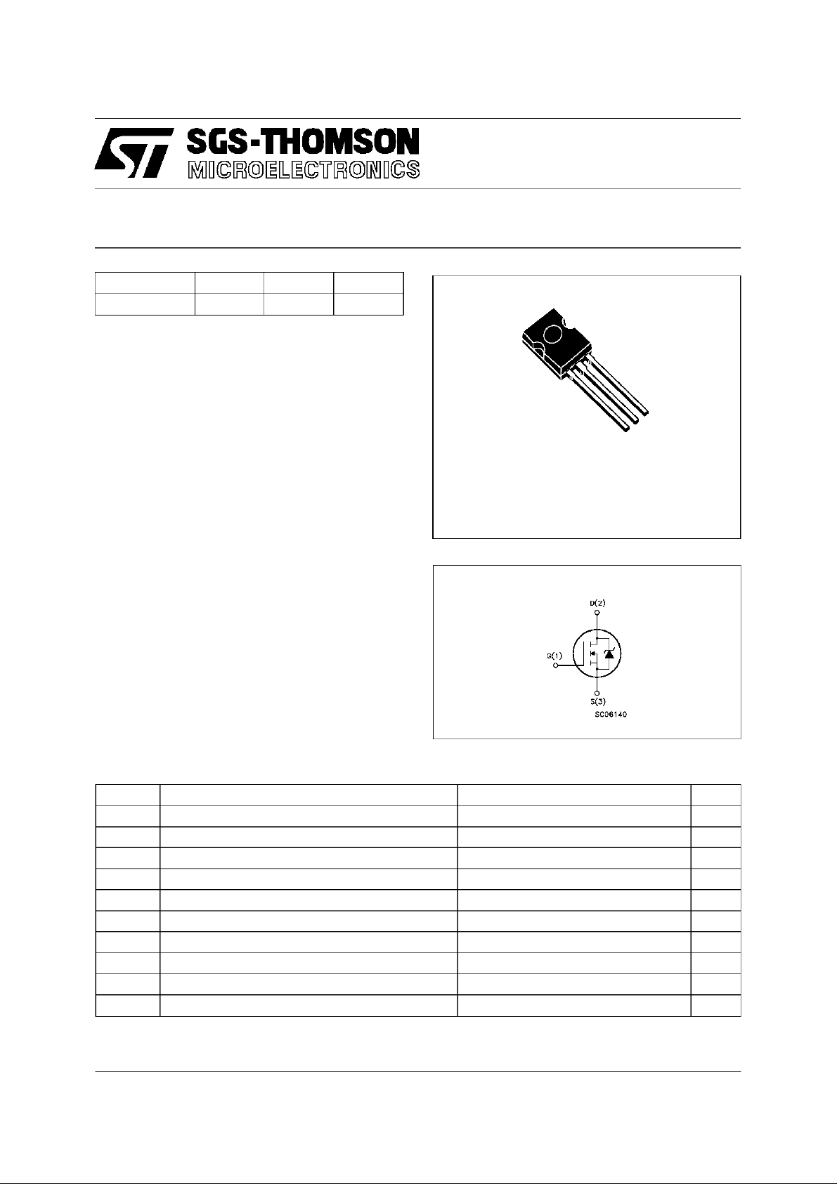
3
2
1
SOT82
INTERNAL SCHEMATIC DIAGRAM
ABSOLUTE MAXIMUM RATINGS
Symb o l Parame t er Val u e Uni t
V
V
DGR
V
I
DM
P
T
(•) Pulse width limited by safe operating area
March 1996
Drain-source Voltage (VGS= 0) 600 V
DS
Drain- gate Voltage (RGS=20kΩ) 600 V
Gate-sourc e Voltage ± 30 V
GS
I
Drain Current (c ont inuo us) a t Tc=25oC2.7A
D
I
Drain Current (c ont inuo us) a t Tc=100oC1.8A
D
(•) Drain Current (puls ed) 10.8 A
Total Dissipat i on at Tc=25oC60W
tot
Derat ing Factor 0.48 W/
Stora ge Temperatu re -65 to 150
stg
T
Max. Operat ing Junc t i on Temperatu r e 150
j
o
C
o
C
o
C
1/9
Page 2
STK3NA60
THERMAL DATA
R
thj-case
R
thj-amb
R
thc-sin k
T
AVALANCHE CHARACTERISTICS
Symb o l Para met er Max Val ue Uni t
I
AR
E
E
I
AR
Ther mal Resistance Junct ion-cas e Max
Ther mal Resistance Junct ion-ambient Max
Ther mal Resistance Case-s i nk Typ
Maximum Lead Tempera t ure For Soldering Purpo se
l
Avalanche Current, Repetitiv e or Not-Repe t it ive
(pulse width lim i t ed by T
Single Pu lse Avalanc he E nerg y
AS
(starti ng T
Repetitive Av alanche Energy
AR
=25oC, ID=IAR,VDD=50V)
j
(pulse width lim i t ed by T
max, δ <1%)
j
max, δ <1%)
j
Avalanche Current, Repetitiv e or Not-Repe t it ive
=100oC, p ulse width lim it ed by Tjmax, δ <1%)
(T
c
2.08
62.5
0.5
300
2.7 A
40 mJ
1.6 mJ
1.8 A
o
C/W
o
C/W
o
C/W
o
C
ELECTRICAL CHARACTERISTICS (T
=25oC unlessotherwise specified)
case
OFF
Symbol Parameter Test Condition s Min. Typ. Max. Unit
V
(BR)DSS
Drain-source
ID= 250 µAVGS= 0 600 V
Break dow n Voltage
I
I
DSS
GSS
Zero Gate Voltage
Drain Current (V
GS
Gat e- bod y Leaka ge
Current (V
DS
=0)
=0)
=MaxRating
V
DS
V
=MaxRatingx0.8 Tc= 125oC
DS
V
= ± 30 V ± 100 nA
GS
250
1000µAµA
ON (∗)
Symbol Parameter Test Condition s Min. Typ. Max. Unit
V
GS(th )
R
DS(on)
I
D(on)
Gat e Thre shold Volt age VDS=VGSID=250µA2.2533.75V
St at ic Drain-source On
Resistance
VGS= 10V ID=1.5A
= 10V ID=1.5A Tc=100oC
V
GS
On State Drain Current VDS>I
D(on)xRDS(on)max
2.9 A
3.3 4
8
VGS=10V
DYNAMIC
Symbol Parameter Test Condition s Min. Typ. Max. Unit
g
(∗)Forward
fs
Tr ansc on ductance
C
C
C
Input Capac it an ce
iss
Out put Capac itance
oss
Reverse Transfer
rss
Capacit a nc e
VDS>I
D(on)xRDS(on)maxID
=1.5A 1 2 S
VDS=25V f=1MHz VGS= 0 380
57
17
500
75
23
Ω
Ω
pF
pF
pF
2/9
Page 3
STK3NA60
ELECTRICAL CHARACTERISTICS (continued)
SWITCHINGON
Symbol Parameter Test Condition s Min. Typ. Max. Unit
t
d(on)
t
r
Turn-on Time
Rise Time
VDD=300V ID=1.5A
=18 Ω VGS=10V
R
G
(see test cir cuit, figure 3)
(di/dt)
Tur n-on C urr ent Slope VDD=400V ID=3A
on
R
=18 Ω VGS=10V
G
(see tes t circuit, f igure 5)
Q
Q
Q
Tot al Gat e Charge
g
Gate-Source Charge
gs
Gat e- Drain Charge
gd
VDD=480V ID=3A VGS=10V 22
SWITCHINGOFF
Symbol Parameter Test Condition s Min. Typ. Max. Unit
t
r(Voff)
t
Off -voltage Rise Time
t
Fall T ime
f
Cross-over T ime
c
VDD=480V ID=3A
=18 Ω VGS=10V
R
G
(see test cir cuit, figure 5)
SOURCE DRAIN DIODE
14
25
20
35
300 A/ µs
30 nC
6
9
13
24
12
18
34
17
ns
ns
nC
nC
ns
ns
ns
Symbol Parameter Test Condition s Min. Typ. Max. Unit
I
I
SDM
SD
Source-drain Current
(•)
Source-drain Current
2.7
10.8
(pulsed)
(∗)ForwardOnVoltage ISD=2.7A VGS=0 1.6 V
V
SD
t
Q
Reverse Recovery
rr
Time
Reverse Recovery
rr
ISD= 3 A di/dt = 100 A/µs
=100V Tj=150oC
V
DD
(see test cir cuit, figure 5)
460
5.6
Charge
I
RRM
Reverse Recovery
24
Current
(∗) Pulsed: Pulse duration =300 µs, duty cycle1.5 %
(•) Pulse width limited by safe operating area
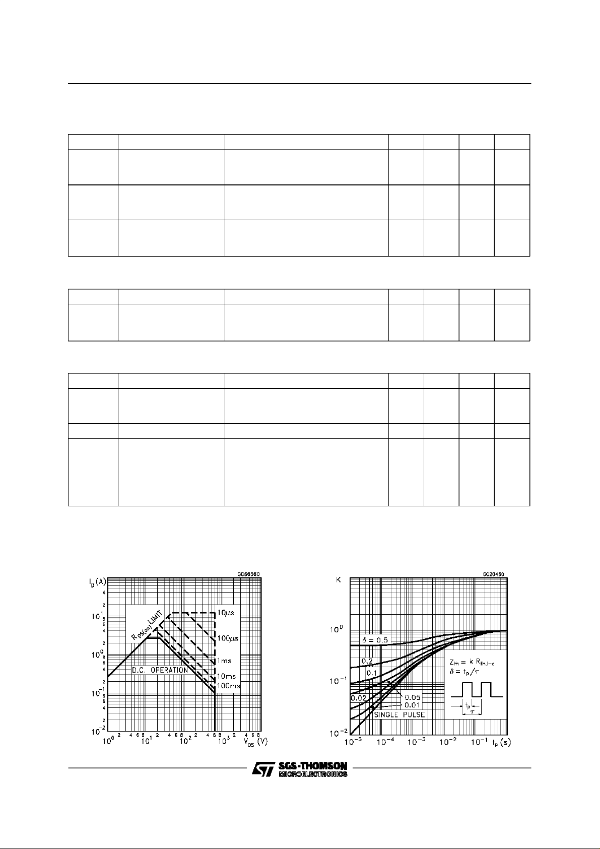
Safe Operating Area ThermalImpedance
A
A
ns
µC
A
3/9
Page 4

STK3NA60
Derating Curve
TransferCharacteristics
OutputCharacteristics
Transconductance
StaticDrain-source On Resistance
4/9
Gate Charge vs Gate-source Voltage
Page 5

STK3NA60
CapacitanceVariations
Normalized OnResistance vs Temperature
Normalized GateThreshold Voltage vs
Temperature
Turn-onCurrent Slope
Turn-offDrain-source VoltageSlope
Cross-overTime
5/9
Page 6

STK3NA60
SwitchingSafe OperatingArea
Source-drainDiode Forward Characteristics
AccidentalOverloadArea
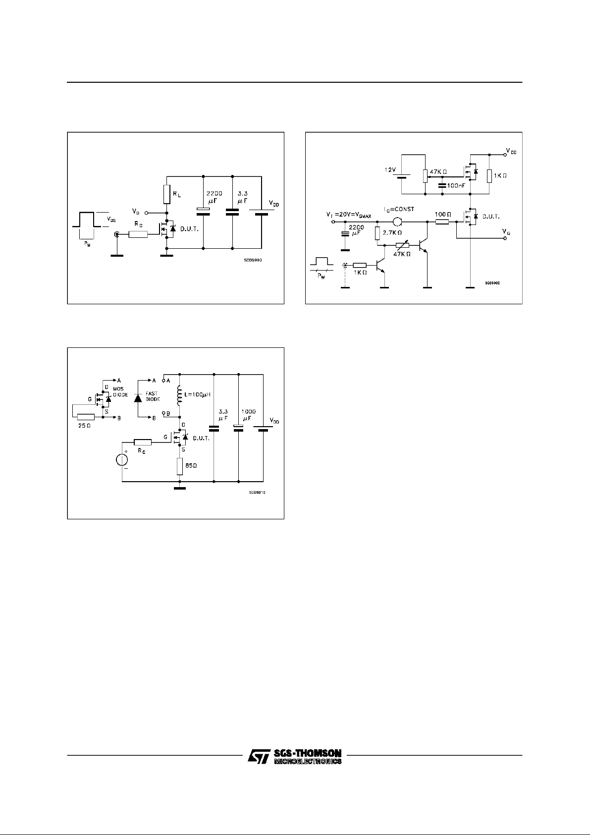
Fig. 1: UnclampedInductive Load Test Circuit
6/9
Fig. 2: UnclampedInductive Waveform
Page 7
STK3NA60
Fig. 3: SwitchingTimes Test Circuits For
ResistiveLoad
Fig. 5: Test CircuitFor InductiveLoad Switching
And DIodeRecovery Times
Fig. 4: GateCharge test Circuit
7/9
Page 8

STK3NA60
SOT-82 MECHANICAL DATA
DIM.
MIN. TYP. MAX. MIN. TYP. MAX.
A 7.4 7.8 0.291 0.307
B 10.5 11.3 0.413 0.445
b 0.7 0.9 0.028 0.035
b1 0.49 0.75 0.019 0.030
C 2.4 2.7 0.04 0.106
c1 1.2 0.047
D 15.7 0.618
e 2.2 0.087
e3 4.4 0.173
F 3.8 0.150
H 2.54 0.100
mm inch
C
c1
b
b1
A
F
BD
H
e
e3
P032A
8/9
Page 9

STK3NA60
Information furnished is believedto be accurateand reliable. However, SGS-THOMSONMicroelectronics assumes no responsability for the
consequencesof use of such information nor forany infringement of patents or otherrights of third parties which may resultsfrom its use. No
licenseis granted by implicationor otherwise underany patentor patent rights ofSGS-THOMSONMicroelectronics.Specificationsmentioned
in this publicationare subject to change without notice. This publication supersedes and replaces all information previously supplied.
SGS-THOMSONMicroelectronics productsare notauthorized for useas criticalcomponents in life supportdevicesor systemswithoutexpress
writtenapproval of SGS-THOMSONMicroelectonics.
1995 SGS-THOMSONMicroelectronics - All RightsReserved
Australia - Brazil - France - Germany- HongKong - Italy- Japan- Korea - Malaysia - Malta- Morocco- TheNetherlands -
Singapore- Spain- Sweden- Switzerland- Taiwan - Thailand - United Kingdom- U.S.A
SGS-THOMSONMicroelectronics GROUP OF COMPANIES
...
9/9
 Loading...