

Page 1
STK3NA50
N - CHANNEL ENHANCEMENT MODE
FAST POWER MOS TRANSISTOR
TYPE V
DSS
R
DS(on)
I
D
STK 3NA50 500 V < 3 Ω 2.7 A
■ TYPICAL R
■ ± 30V GATE TO SOURCE VOLTAGE RATING
■ 100% AVALANCHE TESTED
■ REPETITIVE AVALANCHE DATA AT 100
■ LOW INTRINSIC CAPACITANCES
■ GATE GHARGE MINIMIZED
■ REDUCED THRESHOLD VOLTAGE SPREAD
DS(on)
= 2.4 Ω
o
C
DESCRIPTION
This series of POWER MOSFETS represents the
most advanced high voltage technology. The optimized cell layout coupled with a new proprietary
edge termination concur to give the device low
R
and gate charge, unequalled ruggedness
DS(on)
and superior switching performance.
APPLICATIONS
■ HIGH CURRENT, HIGH SPEED SWITCHING
■ SWITCH MODE POWERSUPPLIES (SMPS)
■ DC-AC CONVERTERS FOR WELDING
EQUIPMENT AND UNINTERRUPTIBLE
POWER SUPPLIES AND MOTOR DRIVE
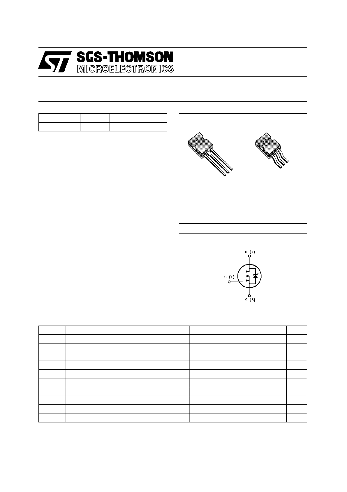
2
3
2
1
1
SOT-82 SOT-194
(option)
INTERNAL SCHEMATIC DIAGRAM
3
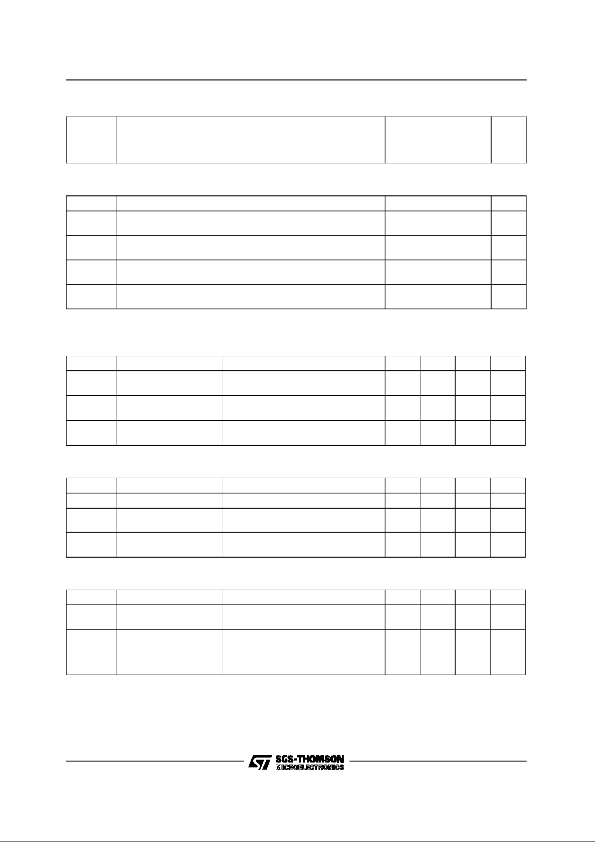
ABSOLUTE MAXIMUM RATINGS
Symb o l Paramet er Val u e Unit
V
V
V
I
DM
P
T
(•) Pulsewidth limited bysafe operating area
November 1996
Drain - s ource Voltage (VGS= 0) 500 V
DS
Drain- gate Voltage (RGS=20kΩ) 500 V
DGR
Gate-source Voltage ± 30 V
GS
Drain Current (continuous) at Tc=25oC2.7A
I
D
Drain Current (continuous) at Tc=100oC1.7A
I
D
(•) Drain Current (pulsed) 10.8 A
Total Di ssipation a t Tc=25oC50W
tot
Derat ing Factor 0.4 W/
St or a ge Tem perature -65 t o 150
stg
Max. Operating Jun ction T emperature 150
T
j
o
o
o
C
C
C
1/10
Page 2
STK3NA50
THERMAL DATA
R
thj-case
R
thj-amb
R
thj-amb
T
AVALANCHE CHARACTERISTICS
Symbol Parameter Max Valu e Uni t
I
AR
E
E
I
AR
Thermal Resistance Junction - cas e Max
Thermal Resistance Junction- ambient Max
Thermal Resistance Case-sink Typ
Maximum L ead Temperat ur e For Soldering Purpos e
l
Avalanc h e Cu rr ent , Repet itive or Not-Rep etitive
(pulse width limited by Tjmax, δ <1%)
Single Pul se Avalanche Ener gy
AS
(starti ng Tj=25oC, ID=IAR,VDD=50V)
Repetitive Avalanc he Energ y
AR
(pulse width limited by Tjmax, δ <1%)
Avalanc h e Cu rr ent , Repet itive or Not-Rep etitive
(Tc= 100oC, pulse width l imited by Tjmax, δ <1%)
2.5
80
0.7
275
2.7 A
40 mJ
2mJ
1.7 A
o
C/W
o
C/W
o
C/W
o
C
ELECTRICAL CHARACTERISTICS (T
=25oC unless otherwisespecified)
case
OFF
Symbol Parameter Test Conditions Min. Typ. Max. Unit
V
(BR)DSS
Drain - s ource
ID=250µAVGS= 0 500 V
Break d own Volta ge
I
DSS
I
GSS
Zer o G at e V oltage
Drain Current (V
GS
Gat e- body Leakage
=0)
=MaxRating
V
DS
V
= Max Rating x 0.8 Tc=125oC
DS
25
250
VGS= ± 30 V ± 100 nA
Current (VDS=0)
ON (∗)
Symbol Parameter Test Conditions Min. Typ. Max. Unit
V
GS(th)
R
DS(on)
Gate Threshold Voltage VDS=VGSID=250µA 2.25 3 3.75 V
St at ic Drain-s our ce O n
VGS=10V ID= 1.5 A 2.4 3 Ω
Resistance
I
D(on)
On State Drain Current VDS>I
D(on)xRDS(on)max
3.3 A
VGS=10V
DYNAMIC
Symbol Parameter Test Conditions Min. Typ. Max. Unit
(∗)Forward
g
fs
Tr ansconductance
C
C
C
Input Capacitance
iss
Out put Capacitance
oss
Reverse Transfer
rss
Capacitance
VDS>I
D(on)xRDS(on)maxID
=1.5A 1.2 2.2 S
VDS=25V f=1MHz VGS=0 370
62
20
485
81
27
µA
µA
pF
pF
pF
2/10
Page 3
STK3NA50
ELECTRICAL CHARACTERISTICS (continued)
SWITCHING ON
Symbol Parameter Test Conditions Min. Typ. Max. Unit
t
d(on)
(di/dt)
Q
Q
Q
Turn-on T ime
t
Rise Time
r
Turn-on Current S lope VDD=400V ID=3A
on
Total Gate Charge
g
Gat e- Source Charge
gs
Gate-Drain Charge
gd
SWITCHING OFF
Symbol Parameter Test Conditions Min. Typ. Max. Unit
t
r(Voff)
t
Off -voltage Rise Time
t
Fall Time
f
Cross-over Time
c
SOURCE DRAINDIODE
VDD=250V ID=1.5A
RG=18 Ω VGS=10V
14
23
(see test circuit, figure 3)
340 A/µs
RG=18 Ω VGS=10V
(see test circuit, figure 5)
VDD= 400 V ID=3A VGS=10V 21
6
9
VDD=400V ID=3A
RG=18 Ω VGS=10V
(see test circuit, figure 5)
13
11
26
20
30
28 nC
18
16
35
ns
ns
nC
nC
ns
ns
ns
Symbol Parameter Test Conditions Min. Typ. Max. Unit
I
I
SDM
SD
Source-drain C urrent
(•)
Source-drain C urrent
2.7
10.8
(pulsed)
V
(∗) Forward On Voltage ISD=2.7A VGS=0 1.6 V
SD
t
Reverse Recovery
rr
Time
Q
Reverse Recovery
rr
ISD=3A di/dt=100A/µs
VDD= 100 V Tj=150oC
(see test circuit, figure 5)
350
4.2
Charge
I
RRM
Reverse Recovery
24
Current
(∗) Pulsed:Pulse duration = 300 µs, dutycycle 1.5 %
(•) Pulse widthlimited by safeoperating area
Safe Operating Area Thermal Impedance
A
A
ns
µC
A
3/10
Page 4

STK3NA50
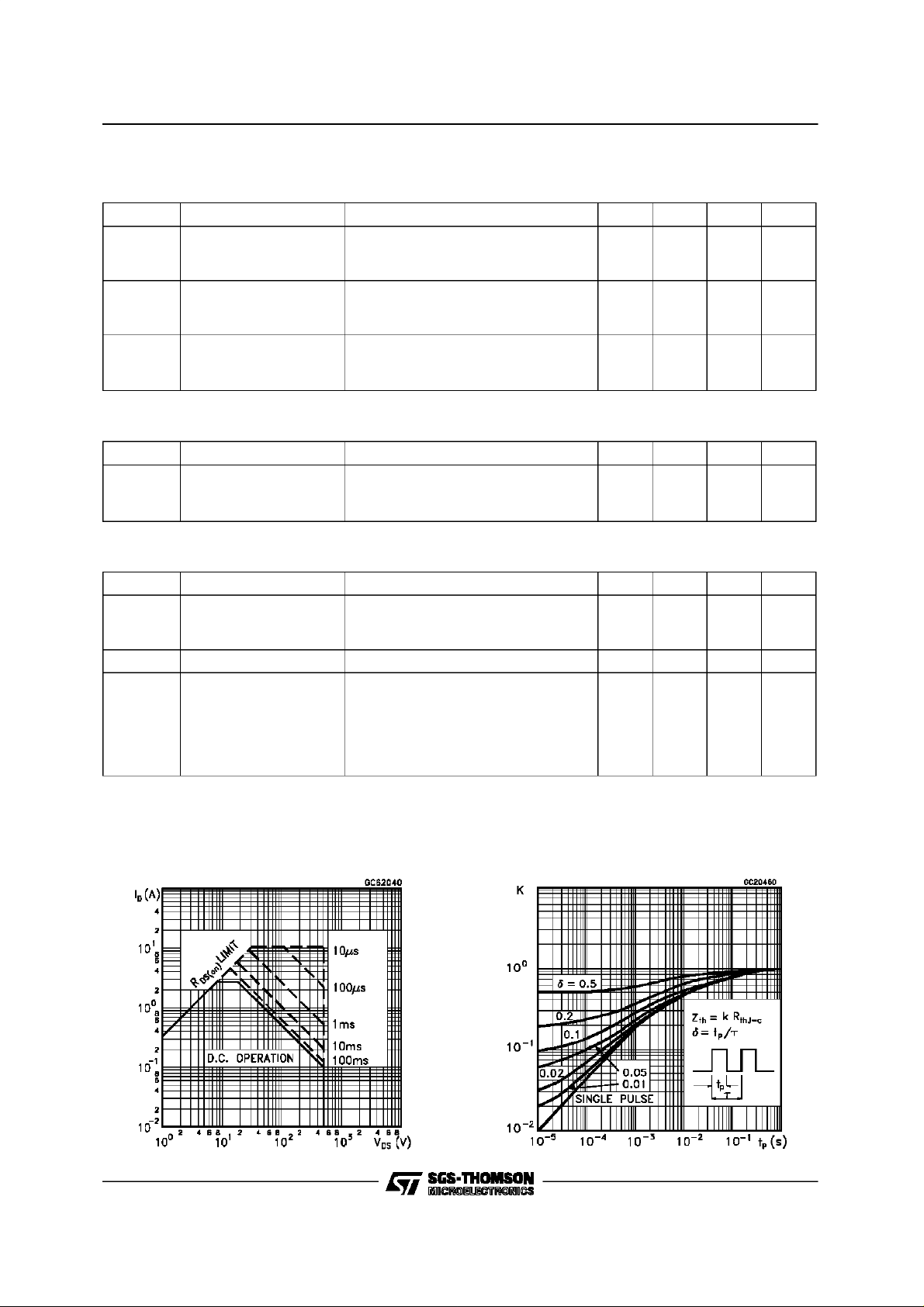
Derating Curve
Transfer Characteristics
Output Characteristics
Transconductance
Static Drain-source On Resistance
4/10
Gate Charge vs Gate-source Voltage
Page 5
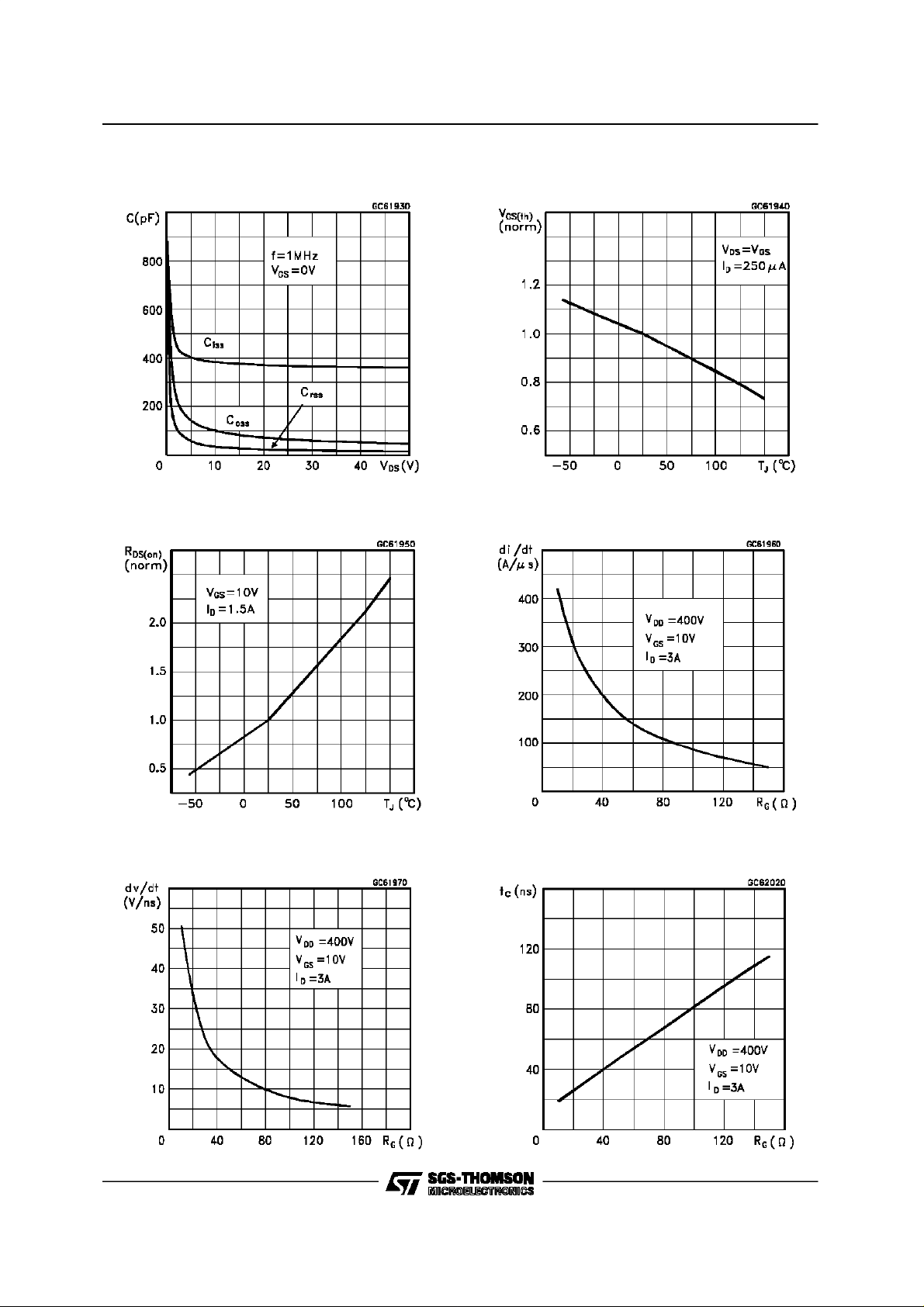
STK3NA50
Capacitance Variations Normalized Gate Threshold Voltage vs
Temperature
Normalized On Resistance vs Temperature Turn-on Current Slope
Cross-over TimeTurn-off Drain-source Voltage Slope
5/10
Page 6

STK3NA50
Switching SafeOperating Area Accidental Overload Area
Source-drain Diode Forward Characteristics
Fig. 1: Unclamped Inductive Load Test Circuits Fig. 2: Unclamped Inductive Waveforms
6/10
Page 7

STK3NA50
Fig. 3: Switching Times Test Circuits For
Resistive Load
Fig. 5: Test Circuit For Inductive Load Switching
And Diode Recovery Times
Fig. 4: Gate Charge Test Circuit
7/10
Page 8

STK3NA50
SOT-82 MECHANICAL DATA
DIM.
MIN. TYP. MAX. MIN. TYP. MAX.
A 7.4 7.8 0.291 0.307
B 10.5 11.3 0.413 0.445
b 0.7 0.9 0.028 0.035
b1 0.49 0.75 0.019 0.030
C 2.4 2.7 0.04 0.106
c1 1.2 0.047
D 15.7 0.618
e 2.2 0.087
e3 4.4 0.173
F 3.8 0.150
H 2.54 0.100
mm inch
C
c1
b
b1
A
F
BD
H
e
e3
P032A
8/10
Page 9

SOT-194 MECHANICAL DATA
STK3NA50
DIM.
MIN. TYP. MAX. MIN. TYP. MAX.
A 7.4 7.8 0.291 0.307
B 10.5 11.3 0.413 0.445
b 0.7 0.9 0.028 0.035
b1 0.49 0.75 0.019 0.030
C 2.4 2.7 0.094 0.106
c1 1.2 0.047
c2 1.3 0.051
D 6 0.236
e 2.2 0.087
e3 4.4 0.173
F 3.8 0.150
H 2.54 0.100
P45°(typ.)
S 4 0.157
S1 2 0.079
T 0.1 0.004
mm inch
C
A
F
B
C1
H
D
b1
T
e
SS1
P
b
c2
e3
P032B
9/10
Page 10

STK3NA50
Information furnished is believed to be accurate and reliable. However, SGS-THOMSON Microelectronics assumes no responsability for the
consequences of use of such information nor for any infringement of patents or other rightsof third parties which mayresults fromits use. No
licenseis granted by implication or otherwise under any patentor patent rights of SGS-THOMSON Microelectronics. Specifications mentioned
in thispublication are subject to change withoutnotice. Thispublication supersedes andreplacesall information previously supplied.
SGS-THOMSONMicroelectronics products are not authorizedfor use ascriticalcomponents in lifesupport devices or systems withoutexpress
writtenapproval ofSGS-THOMSONMicroelectonics.
1996 SGS-THOMSON Microelectronics -Printed in Italy- AllRightsReserved
Australia- Brazil -Canada -China - France- Germany - HongKong- Italy - Japan- Korea- Malaysia - Malta- Morocco - The Netherlands -
Singapore - Spain - Sweden - Switzerland-Taiwan - Thailand- UnitedKingdom - U.S.A
SGS-THOMSONMicroelectronics GROUPOF COMPANIES
.
10/10
 Loading...