

Page 1
Overview
The STK301-220 is a hybrid IC (HIC) for electronically
controlled graphic equalizer applications and is equipped
with on-chip electronic volume control for 7-band, 2channel graphic equalization, thereby permitting onetouch up-down control of all band gains. The STK301220 is a hybrid IC which combines SC system and
photoresist techniques with folded board construction
while incorporating Sanyo’s unique insulated metal
substrate technology (IMST) to the base.
Applications
• Car stereos
• Portable radio-cassette players
• Home stereos
Features
• All bands are set for L/R simultaneous 2 dB incremental
operation (typ).
• All bands are equipped with 13 positions and range
between +12 dB maximum boost to –12 dB maximum cut.
• Crossover frequencies include fo; 60 Hz, 150 Hz,
400 Hz, 1 kHz, 2.5 kHz, 6 kHz and 15 kHz.
• The following features can be made available with an
electronic graphic equalizer system which incorporates
the 3-IC construction consisting of the STK301-220, a
controller (universal microcontroller) along with the
display LSI (LC75821→LCD, LC7565→FLT, LED):
— One-touch up-down control of all band gains.
—
Immediate recall of preferred frequency levels tailored
to suit musical selections. This is possible using preset
functions to retrieving items from one-touch memory
.
— Such functions as setting all bands to 0 dB (flat
function), or switching frequency characteristics
from 0 dB to center (reverse function) may be
simply performed with supported software.
— Dual control lines permit mutual use with display
LSI and help to simplify wiring between
microcontroller and LSI.
• Minimal operating shock noise when boost or cut is used.
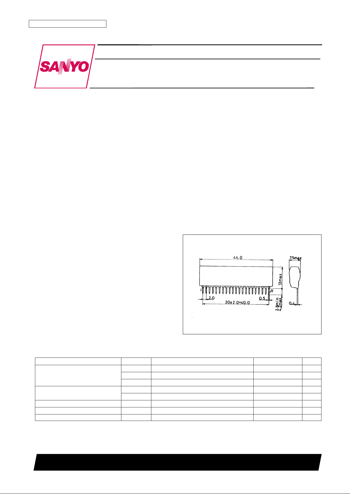
Package Dimensions
unit : mm
4143
Thick-Film Hybrid IC
N3096HA (OT)/82294TH (OT) 5-3398 No. 4793-1/8
[STK301-220]
SANYO Electric Co.,Ltd. Semiconductor Bussiness Headquarters
TOKYO OFFICE Tokyo Bldg., 1-10, 1 Chome, Ueno, Taito-ku, TOKYO, 110 JAPAN
7-band, 2-channel Electronic Graphic Equalizer
STK301-220
Ordering number : EN4793A
Specifications
Maximum Ratings at Ta = 25°C, VSS= 0 V
Parameter Symbol Conditions Ratings Unit
V
DD-VEE
max 16 V
Maximum supply voltage V
CC
1 max ±18 (36) V
V
CC
2 max 7V
Input voltage
V
I
1 CLK, DI, IN1, IN2 0 to VCC2 + 0.3 V
V
I
2 CLK, DI, IN1, IN2 VEE– 0.3 to VDD+ 0.3 V
Allowable power dissipation Pd max 920 mW
Operating temperature Topr –20 to +70 °C
Storage temperature Tstg –40 to +100 °C
Page 2
No. 4793-2/8
STK301-220
Recommended Operational Voltage at Ta = 25°C
Parameter Symbol Conditions Ratings Unit
V
DD/VEEVSS
= 0 V ±7 (14) V
Supply voltage V
CC
1 VSS= 0 V ±7 (14) V
V
CC
2 VSS= 0 V 5 V
Allowable Operating Ranges at Ta = 25°C, VSS= 0 V
Parameter Symbol Conditions Ratings Unit
V
DD-VEE
7.5 to 15.0 V
Supply voltage V
CC
1 ±4 to ±18 (8 to 36) V
V
CC
2 4.5 to 5.5 V
Input high level voltage V
IH
CLK, DI 0.8 VCC2 to VCC2 V
Input low level voltage V
IL
CLK, DI 0.2 VCC2 V
Input pulse width t
ØW
CLK from 1 µs
Setup time t
setup
DI from 1 µs
Hold time t
hold
DI from 1 µs
Operating frequency f
opg
CLK up to 330 kHz
Operating Characteristics at Ta = 25°C, VSS= 0 V, VDD/V
EE
= ±7 V, VCC1 = ±7 V, VCC2 = 5 V, f = 1 kHz
All bands flat, using the specified test circuit
Parameter Symbol Conditions
Ratings
Unit
min typ max
I
DD
VDD/VEE= ±7 V, VCC1 = ±7 V,VSS= 0 V
1 mA
Current dissipation I
CC
1
V
CC
2 = 5 V
20 30 mA
I
CC
2 1 mA
Voltage gain VG V
IN
= –10 dB–4.0 –1.0 +2.0 dB
Total harmonic distortion THD f = 1 kHz, V
O
= 1V, 30 kHz L.P.F 0.005 0.1 %
Crosstalk C.T. f = 20 kHz, V
IN
= 0 dB 45 55 dB
Output noise voltage V
NO
Rg = 0 Ω, 10 Hz to 30 kHz B.P.F 9 25 µV
Setting error ∆B –1 +1 dB
f (1) f = 60 Hz ±10 ±12 ±14 dB
f (2) f = 150 Hz ±10 ±12 ±14 dB
f (3) f = 400 Hz
When operating at f = 1 kHz,
±10 ±12 ±14 dB
Frequency response f (4) f = 1 kHz all bands are flat and ±10 ±12 ±14 dB
f (5) f = 2.5 kHz
V
O
= –10 dB set at 0 dB.
±10 ±12 ±14 dB
f (6) f = 6 kHz ±10 ±12 ±14 dB
f (7) f = 15 kHz ±10 ±12 ±14 dB
Note: With constant voltage power supply.
The supply voltage figures in parentheses indicate the voltages when a single voltage power supply is used.
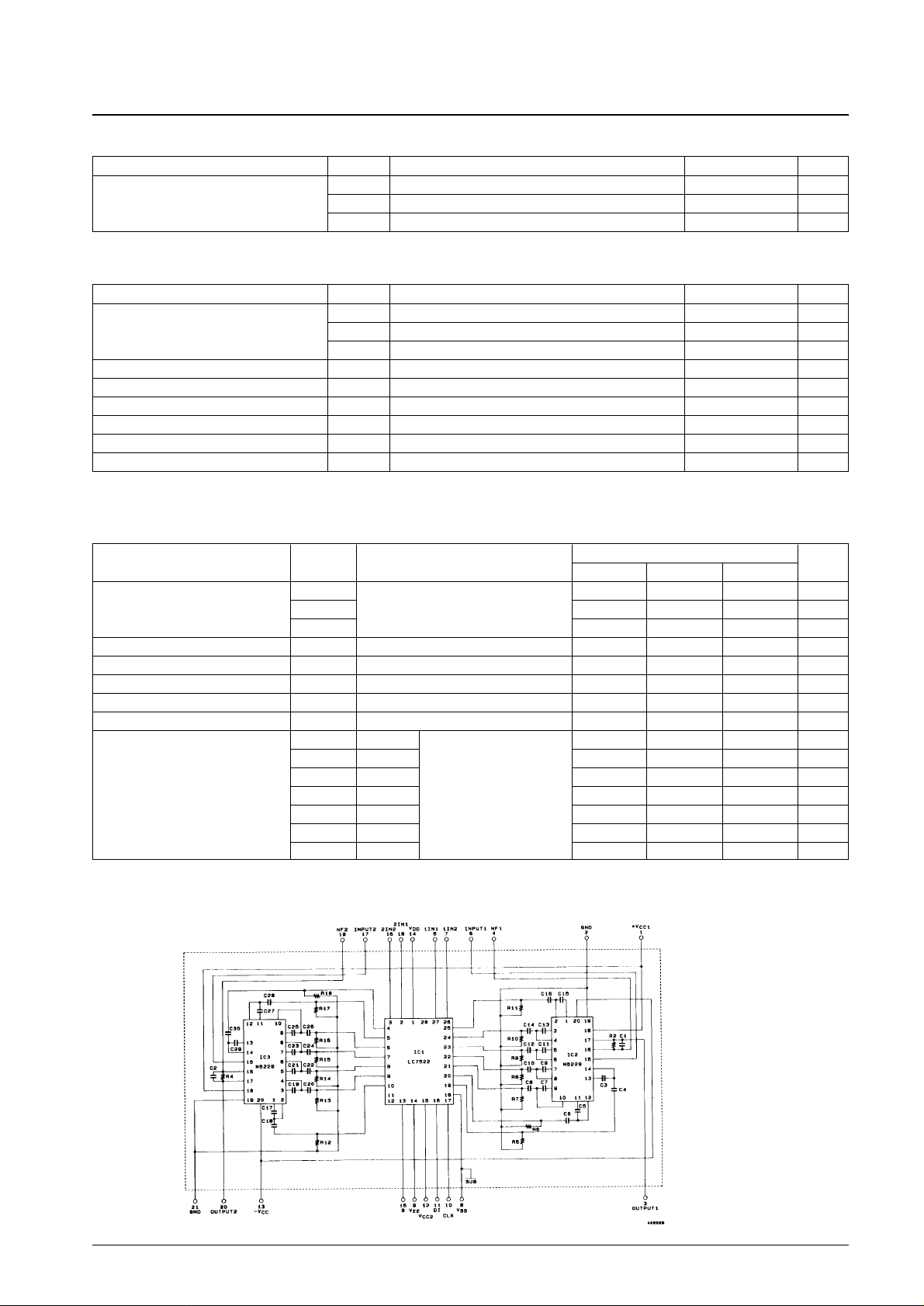
Internal Equivalent Circuit
Page 3
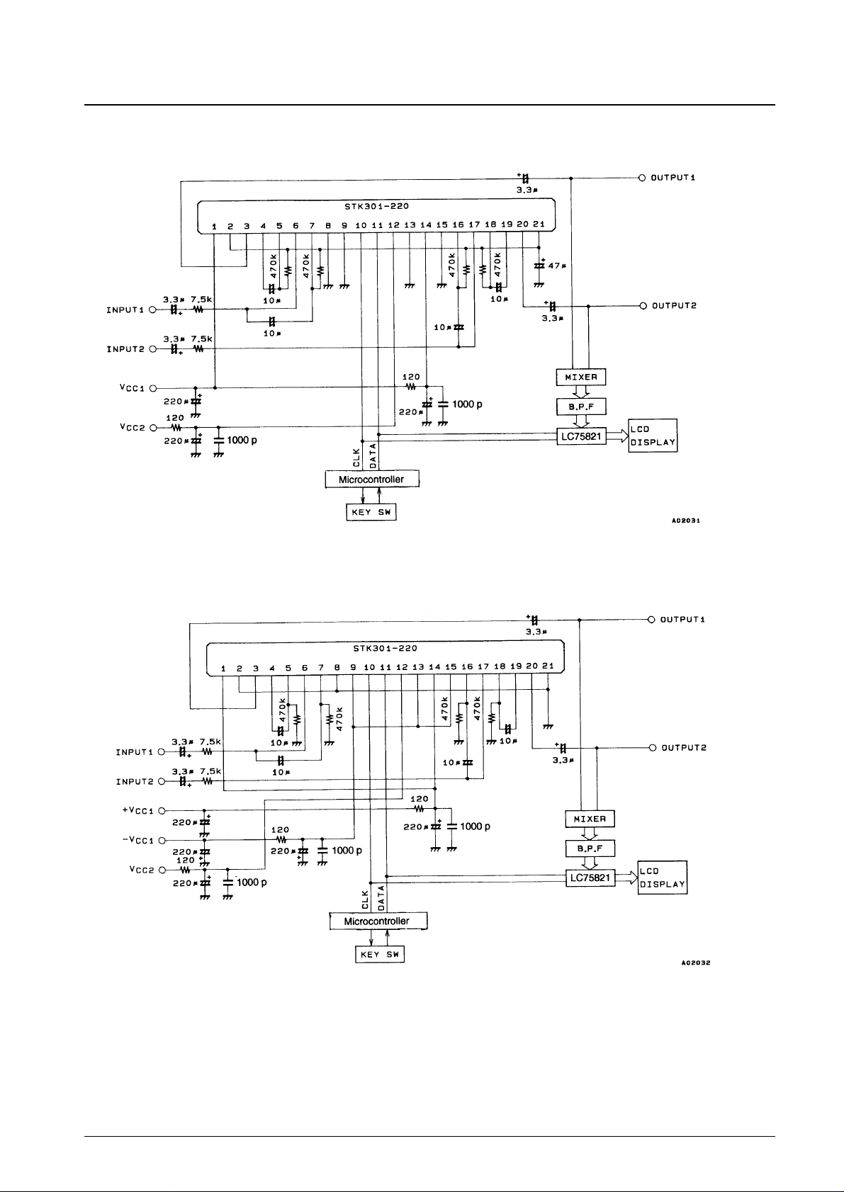
Sample Application Circuit
Single Power Supply
Split Power Supply
Unit (resistance: Ω, capacitance:F)
Unit (resistance: Ω, capacitance:F)
No. 4793-3/8
STK301-220
Page 4

No. 4793-4/8
STK301-220
Pin Descriptions
Pin No. Pin name Functions
1 +V
CC
1 Power supply pin used for + power supply to IC2 and IC3 graphic equalizer.
2, 21 DC
Pin for 1/2 V
CC
1 decoupling capacitor of graphic equalizer IC. When shortened, power supply becomes more effective and
ripples are vulnerable.
3 OUTPUT 1 Output pin 1.
4 NF 1 Inverting input for the graphic equalizer IC2 internal operational amplifier.
5 1IN 1 Audio signal input 1 (INPUT1) for electronic volume control IC1
6 INPUT 1 Input impedance for input pin 1 rated at approximately 60 kΩ (1 kHz, flat).
7 1IN 2 Audio signal input 2 (INPUT1) for electronic volume control IC1
8 V
SS
Power supply pin connected to ground (GND).
9 V
EE
Power supply pin used for audio signal power supply to electronic volume control section. When single power supply is used,
connect to V
SS
.
10 CLK Input pin for data from CPU according to Schmitt inverter format.
11 DI Input pin for clock from the CPU according to Schmitt inverter format.
12 +V
CC
2 Power supply pin rated at +5 V (typ). Make sure that VCC2 does not onset before VDD.
13 GND (–V
CC
1) Power supply pin for ground (- power supply) of IC2 and IC3 graphic equalizer.
14 V
DD
Power supply pin used for audio signal power supply to electronic volume control section.
Select pin for applications using two ICs. Input “1” to initiate key code 7C3 for
15 S
connecting to V
DD
. Input “0” to initiate key code 7C2 for connecting to VEE.
16 2IN 2 Audio signal input 2 (INPUT2) for electronic volume control IC1
17 INPUT 2 Input impedance for input pin 2 rated at approximately 60 kΩ (1 kHz, flat).
18 2IN 1 Audio signal input 1 (INPUT2) for electronic volume control IC1
19 NF 2 Inverting input for the graphic equalizer IC3 internal operational amplifier.
20 OUTPUT 2 Output pin 2.
Note: Refer to LC7522 or LC7523 specifications concerning pins which do not appear here and are hybrid IC (HIC) pins connected directly to a LC7522 or
LC7523 pins.
Description of Operation
The STK301-220 is a hybrid IC (HIC) with a 7-component 2-channel construction for electronically controlled graphic
equalizer applications. It employs an LC7522 for graphic equalizer electronic volume control and an M5229 for 7component graphic equalizer functions.
Figure 1 Equivalent Circuit Block Diagram
Page 5

Pins f (1) through f (7) are used as pin connections for the
LC7522 band filter. Supported frequencies and their pin
assignments are listed in the following.
Pin Name Frequency
f (1) 60Hz
f (2) 150Hz
f (3) 400Hz
f (4) 1kHz
f (5) 2.5kHz
f (6) 6kHz
f (7) 15kHz
In order to minimize the noise which occurs during changeover,
connections are made using 1 MΩ resistors from pins f (1)
through f (7) to 1/2 VCC1.
Resistor Equivalent Circuit
(single band)
Principles of Operation
The graphic equalizer section is constructed from 7 resonance circuits and output buffer amplifiers (every channel);
variable resistors (LC7522) and resonance circuit capacitors C1 and C2 are built-in. Resonance circuits utilize
semiconductor inductors and apply resonation to reduced impedance; all frequency gains are altered.
1. Resonance Circuit
Semiconductor inductors replace the L of the R, L, C series
resonance circuit with a CR element passing through the
buffer function of active elements such as the transistor and
op-amp (operational amplifier), thereby effecting the
equivalent operation of a R, L, C series resonance circuit.
The STK301-220 resonance circuit buffer is constructed
using transistors and arranged as illustrated in Figure 2.
Resonance frequency fo is determined using the following
formula:
fo =
Figure 2 Resonance Circuit
2. Flat, Boost and Cut
Gains matching resonance circuit frequency gains are altered
by altering the built-in resonance circuits and electronic
volume control. Figure 3 is presented to describe the
equivalent circuit. Z represents the impedance of the
resonance circuit in Figure 2.
Figure 3 Equivalent Circuit
No. 4793-5/8
STK301-220
2π1C1 · C2 · R1 · R2
Page 6

No. 4793-6/8
STK301-220
3. Flat
When the volume control is set to the midrange
position and Ri=RNF, the following relationships are
established:
ei' =
R/2
· ei
Ri = R/2
AV=
RNF+ R/2
R/2
in which
eo = AV·ei' = ei
with no relation to the resonance circuit and frequency
characteristics become flat.
When VR is set to R, the resistance value using the VR
center position becomes R/2.
4. Boost
When the volume control is set to the boost position, the resonance circuit is linked to the NF loop of the output
buffer amplifier. Under these circumstances and when R»Ri and RNF, the following relationship exist:
AV=
RNF+ Z
Z
is established and output voltageeo is calculated as
eo = AV·ei =
R
NF
+ Z
· ei
Z
The gain becomes a minimum when the resonance circuit
has Z at a minimum so that the frequency option is boosted.
5. Cut
When volume is set to the cut side, resonance circuit is linked to the input side of the output buffer amplifier. Under
these circumstances and when ignoring R similarly to boost, the following relationship exist:
ei' =
Z
· ei, AV= 1
Ri+Z
is established and output voltage eo is calculated as
eo = AV·ei' =
Z
· ei
Ri+Z
The gain becomes a minimum when the resonance circuit
has Z at a minimum so that the frequency option is cut.
6. Resonance Circuit Crest Acuteness (Q)
Resonance circuit crest acuteness is determined by
comparing frequency widths ω2 - ω1 for GVmax/√2 where
GVmax represents point ω0 as the maximum value of the
resonance circuit crest.
The following formula is used to calculate the value for Q:
Q =
As the value for Q becomes larger, the participating frequency bandwidth of the resonance circuit becomes narrower.
Although neighboring bands distinction is precise, the swell of frequency characteristics under total boost is larger
while the peak of the resultant frequency is lowered.
C1 · R2
C2 · R1
Page 7

With the STK301-220, few crossover bands exist with an increase in swell during total boost. Pass-band-ripple
(P.B.R.) width at this time is 4 dB with Q set at 3.5 fore and aft.
Data Code
1. Turning on the power initiates a process which transmits no
data (0) for 60 clock cycles (initialization clock). When data
is stopped en route, the remaining data is sent only after the
clock has been initialized.
2. Using DI and CLK in conjunction with LC75821 (or
equivalent) involves the transmission of the maximum
initialization clock to those devices involved.
Things to Note
1. A 1000pF rated capacitor (or higher) should be installed between the current pin and VSS.
2. When the control signal on the microcontroller side onsets faster than STK301-220’s VDD, a resistor rated at
2 kΩ or more should be placed on the DI and CLK line.
3. Since the STK301-220 is equipped with a built-in CMOS LSI, sufficient caution should be extended to damage
caused by static electricity.
4. Refer to the specification sheet for itemized details about the LC7522.
No. 4793-7/8
STK301-220
Page 8

No. 4793-8/8
STK301-220
This catalog provides information as of August, 1997. Specifications and information herein are subject to
change without notice.
■ No products described or contained herein are intended for use in surgical implants, life-support systems, aerospace
equipment, nuclear power control systems, vehicles, disaster/crime-prevention equipment and the like, the failure of
which may directly or indirectly cause injury, death or property loss.
■ Anyone purchasing any products described or contained herein for an above-mentioned use shall:
➀ Accept full responsibility and indemnify and defend SANYO ELECTRIC CO., LTD., its affiliates, subsidiaries and
distributors and all their officers and employees, jointly and severally, against any and all claims and litigation and all
damages, cost and expenses associated with such use:
➁ Not impose any responsibility for any fault or negligence which may be cited in any such claim or litigation on
SANYO ELECTRIC CO., LTD., its affiliates, subsidiaries and distributors or any of their officers and employees
jointly or severally.
■ Information (including circuit diagrams and circuit parameters) herein is for example only; it is not guaranteed for
volume production. SANYO believes information herein is accurate and reliable, but no guarantees are made or implied
regarding its use or any infringements of intellectual property rights or other rights of third parties.
 Loading...