

Page 1
STK2N80
N - CHANNEL ENHANCEMENT MODE
POWER MOS TRANSISTOR
TYPE V
DSS
R
DS(on)
I
D
STK 2N80 800 V < 7 Ω 2.1 A
■ TYPICAL R
■ AVALANCHE RUGGED TECHNOLOGY
■ 100% AVALANCHE TESTED
■ REPETITIVE AVALANCHE DATA AT 100
■ LOW INPUT CAPACITANCE
■ LOW GATE CHARGE
■ APPLICATION ORIENTED
DS(on)
=5Ω
o
C
CHARACTERIZATION
APPLICATIONS
■ HIGH CURRENT, HIGH SPEED SWITCHING
■ SWITCH MODE POWERSUPPLIES (SMPS)
■ CONSUMER AND INDUSTRIAL LIGHTING
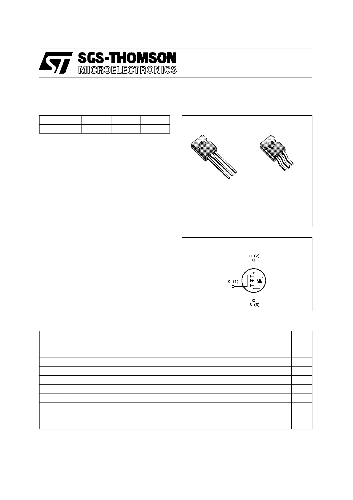
2
3
2
1
1
SOT-82 SOT-194
(option)
INTERNAL SCHEMATIC DIAGRAM
3
ABSOLUTE MAXIMUM RATINGS
Symb o l Paramet er Val u e Unit
V
V
V
I
DM
P
T
(•) Pulsewidth limited bysafe operating area
December 1996
Drain - s ource Voltage (VGS= 0) 800 V
DS
Drain- gate Voltage (RGS=20kΩ) 800 V
DGR
Gate-source Voltage ± 20 V
GS
Drain Current (continuous) at Tc=25oC2.1A
I
D
Drain Current (continuous) at Tc=100oC1.3A
I
D
(•) Drain Current (pulsed) 9.6 A
Total D i ssipation at Tc=25oC70W
tot
Derat ing Factor 0.56 W/
St or a ge Tem perature -65 to 150
stg
Max. Operating Junctio n Temperatur e 150
T
j
o
o
o
C
C
C
1/10
Page 2
STK2N80
THERMAL DATA
R
thj-case
R
thj-amb
R
thj-amb
T
AVALANCHE CHARACTERISTICS
Symbol Parameter Max Valu e Uni t
I
AR
E
E
I
AR
Thermal Res istance Junction -c as e Max
Thermal Resis tance Junction- ambient Max
Thermal Res istance Case-sink Typ
Maximum Lead Temperature For Soldering Purpose
l
Avalanc h e Cu rr ent , Repet itive or Not-R epetitive
(pulse width limited by Tjmax, δ <1%)
Single Pul se Avalanche Ener gy
AS
(starti ng Tj=25oC, ID=IAR,VDD=25V)
Repetitive Avalanc he Energ y
AR
(pulse width limited by Tjmax, δ <1%)
Avalanc h e Cu rr ent , Repet itive or Not-R epetitive
(Tc= 100oC, puls e width limited by Tjmax, δ <1%)
1.78
80
0.7
275
2.1 A
80 mJ
2.8 mJ
1.3 A
o
C/W
o
C/W
o
C/W
o
C
ELECTRICAL CHARACTERISTICS (T
=25oC unless otherwise specified)
case
OFF
Symbol Parameter Test Condition s Min. Typ. Max. Unit
V
(BR)DSS
Drain - s ource
ID=250µAVGS= 0 800 V
Break d own Volta ge
I
DSS
I
GSS
Zer o Gate Voltage
Drain Current (V
GS
Gat e- body Leakage
=0)
=MaxRating
V
DS
V
= Max R ating x 0.8 Tc=125oC
DS
25
250
VGS= ± 20 V ± 100 nA
Current (VDS=0)
ON (∗)
Symbol Parameter Test Condition s Min. Typ. Max. Unit
V
GS(th)
R
DS(on)
Gate Threshold V oltage VDS=VGSID=250µA234V
St at ic Drain-s our ce O n
VGS=10V ID=1A 5 7 Ω
Resistance
I
D(on)
On St ate Dra in Current VDS>I
D(on)xRDS(on)max
2.1 A
VGS=10V
DYNAMIC
Symbol Parameter Test Condition s Min. Typ. Max. Unit
(∗)Forward
g
fs
Tr ansconductance
C
C
C
Input Capacitance
iss
Out put Capacitance
oss
Reverse Transfer
rss
Capacitance
VDS>I
D(on)xRDS(on)maxID
=1A 1.2 1.9 S
VDS=25V f=1MHz VGS=0 460
55
22
600
70
30
µA
µA
pF
pF
pF
2/10
Page 3
STK2N80
ELECTRICAL CHARACTERISTICS (continued)
SWITCHING ON
Symbol Parameter Test Condition s Min. Typ. Max. Unit
t
d(on)
(di/dt)
Q
Q
Q
Turn-on Time
t
Rise Time
r
Turn-on C urrent Slope VDD=640V ID=2A
on
Total Gate Charge
g
Gat e- Source Charge
gs
Gate-Drain Charge
gd
SWITCHING OFF
Symbol Parameter Test Condition s Min. Typ. Max. Unit
t
r(Voff)
t
Off -voltage R ise Time
t
Fall Time
f
Cross-over Time
c
SOURCE DRAIN DIODE
VDD=400V ID=1.5A
RG=50 Ω VGS=10V
38
42
(see test circuit, figure 3)
160 A/µs
RG=50 Ω VGS=10V
(see test circuit, figure 5)
VDD= 640 V ID=2A VGS=10V 31
6
14
VDD=640V ID=2A
RG=50 Ω VGS=10V
(see test circuit, figure 5)
70
25
108
50
57
40 nC
90
32
140
ns
ns
nC
nC
ns
ns
ns
Symbol Parameter Test Condition s Min. Typ. Max. Unit
I
I
SDM
SD
Source-drain Current
(•)
Source-drain Current
2.1
9.6
(pulsed)
V
(∗) For w ar d On Volt age ISD=2.1A VGS=0 2 V
SD
t
Reverse Recovery
rr
Time
Q
Reverse Recovery
rr
ISD= 2 A di/dt = 100 A/µs
VDD= 100 V Tj=150oC
(see test circuit, figure 5)
920
18.4
Charge
I
RRM
Reverse Recovery
40
Current
(∗) Pulsed:Pulse duration = 300 µs, dutycycle 1.5 %
(•) Pulse widthlimited by safeoperating area
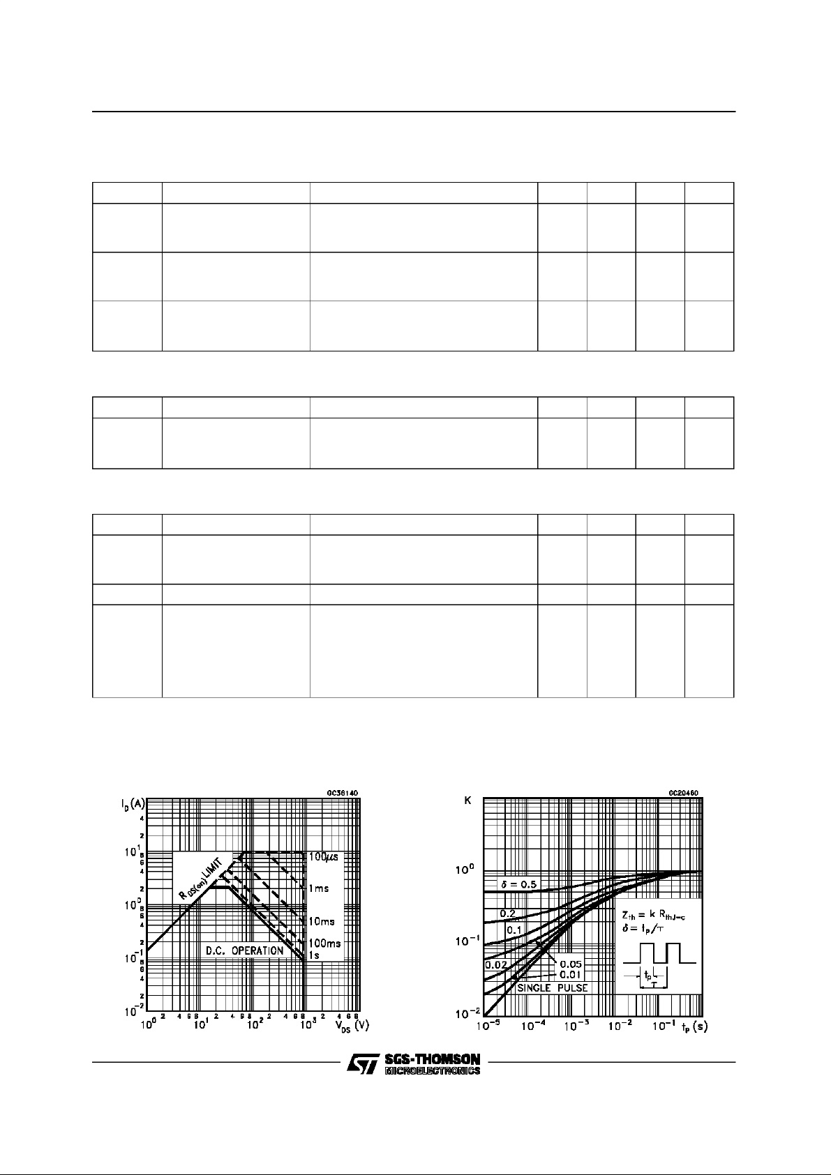
Safe Operating Area Thermal Impedance
A
A
ns
µC
A
3/10
Page 4

STK2N80
Derating Curve
Transfer Characteristics
Output Characteristics
Transconductance
Static Drain-source On Resistance
4/10
Gate Charge vs Gate-source Voltage
Page 5

Capacitance Variations Normalized Gate Threshold Voltage vs
Temperature
Normalized On Resistance vs Temperature Turn-on Current Slope
STK2N80
Cross-over TimeTurn-off Drain-source Voltage Slope
5/10
Page 6

STK2N80
Switching SafeOperating Area Accidental Overload Area
Source-drain Diode Forward Characteristics
Fig. 1: Unclamped Inductive Load Test Circuits Fig. 2: Unclamped Inductive Waveforms
6/10
Page 7

STK2N80
Fig. 3: Switching Times Test Circuits For
Resistive Load
Fig. 5: Test Circuit For Inductive Load Switching
And Diode Recovery Times
Fig. 4: Gate Charge Test Circuit
7/10
Page 8

STK2N80
SOT-82 MECHANICAL DATA
DIM.
MIN. TYP. MAX. MIN. TYP. MAX.
A 7.4 7.8 0.291 0.307
B 10.5 11.3 0.413 0.445
b 0.7 0.9 0.028 0.035
b1 0.49 0.75 0.019 0.030
C 2.4 2.7 0.04 0.106
c1 1.2 0.047
D 15.7 0.618
e 2.2 0.087
e3 4.4 0.173
F 3.8 0.150
H 2.54 0.100
mm inch
C
c1
b
b1
A
F
BD
H
e
e3
P032A
8/10
Page 9

SOT-194 MECHANICAL DATA
STK2N80
DIM.
MIN. TYP. MAX. MIN. TYP. MAX.
A 7.4 7.8 0.291 0.307
B 10.5 11.3 0.413 0.445
b 0.7 0.9 0.028 0.035
b1 0.49 0.75 0.019 0.030
C 2.4 2.7 0.094 0.106
c1 1.2 0.047
c2 1.3 0.051
D 6 0.236
e 2.2 0.087
e3 4.4 0.173
F 3.8 0.150
H 2.54 0.100
P45°(typ.)
S 4 0.157
S1 2 0.079
T 0.1 0.004
mm inch
C
A
F
B
C1
H
D
b1
T
e
SS1
P
b
c2
e3
P032B
9/10
Page 10

STK2N80
Information furnished is believed to be accurate and reliable. However, SGS-THOMSON Microelectronics assumes no responsability for the
consequences of use of such information nor for any infringement ofpatents or other rights of third parties which mayresults from its use. No
licenseis granted by implicationor otherwise under any patentor patentrights of SGS-THOMSON Microelectronics. Specifications mentioned
in thispublication aresubject tochange withoutnotice. This publicationsupersedes and replaces allinformation previously supplied.
SGS-THOMSON Microelectronics products are notauthorizedfor use ascriticalcomponents in lifesupportdevices orsystemswithout express
writtenapproval of SGS-THOMSONMicroelectonics.
1996 SGS-THOMSONMicroelectronics - Printed in Italy- All Rights Reserved
Australia- Brazil - Canada -China - France- Germany - HongKong- Italy- Japan- Korea- Malaysia - Malta - Morocco - The Netherlands-
Singapore - Spain- Sweden- Switzerland- Taiwan- Thailand- United Kingdom - U.S.A
SGS-THOMSONMicroelectronics GROUP OF COMPANIES
.
10/10
 Loading...