

Page 1
STE53NC50
N-CHANNEL 500V - 0.070Ω - 53A ISOTOP
PowerMesh™II MOSFET
TYPE V
STE53NC50 500V < 0.08Ω 53 A
n
TYPICAL RDS(on) = 0.07 Ω
n
EXTREMELY HIGH dv /d t C APABILITY
n
100% AVALANCHE TESTED
n
NEW HIGH VOLTAGE BENCHMARK
n
GATE CHARGE MINIMIZED
DSS
R
DS(on)
I
D
DESCRIPTION
The PowerMESH
generation of MESH OVERLAY
™II is the evolution of the first
™. The layout re-
finements introduced greatly improve the Ron*area
figure of merit while keeping the device at the lea ding edge for what concerns swithing speed, gate
charge and ruggedness.
APPLICATIONS
n
HIGH CURRENT, HIGH SPEED SWITCHING
n
SWITH MODE POWER SUPPLI ES (SMPS)
n
DC-AC CONVERTERS FOR WELDING
EQUIPMENT AND UNINTERRUPTIBLE
POWER SUPPLIES AND MOTOR DRIVER
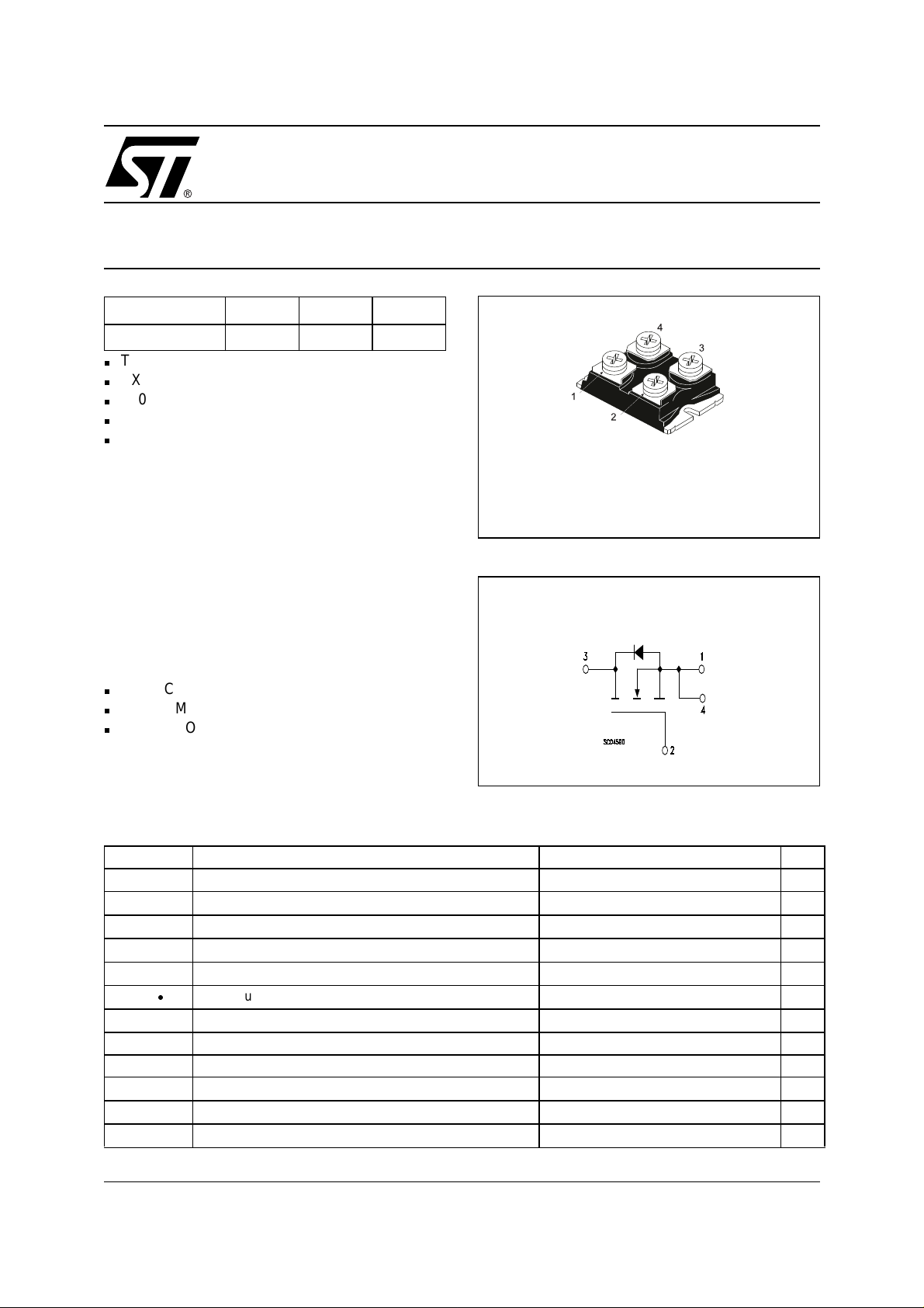
ISOTOP
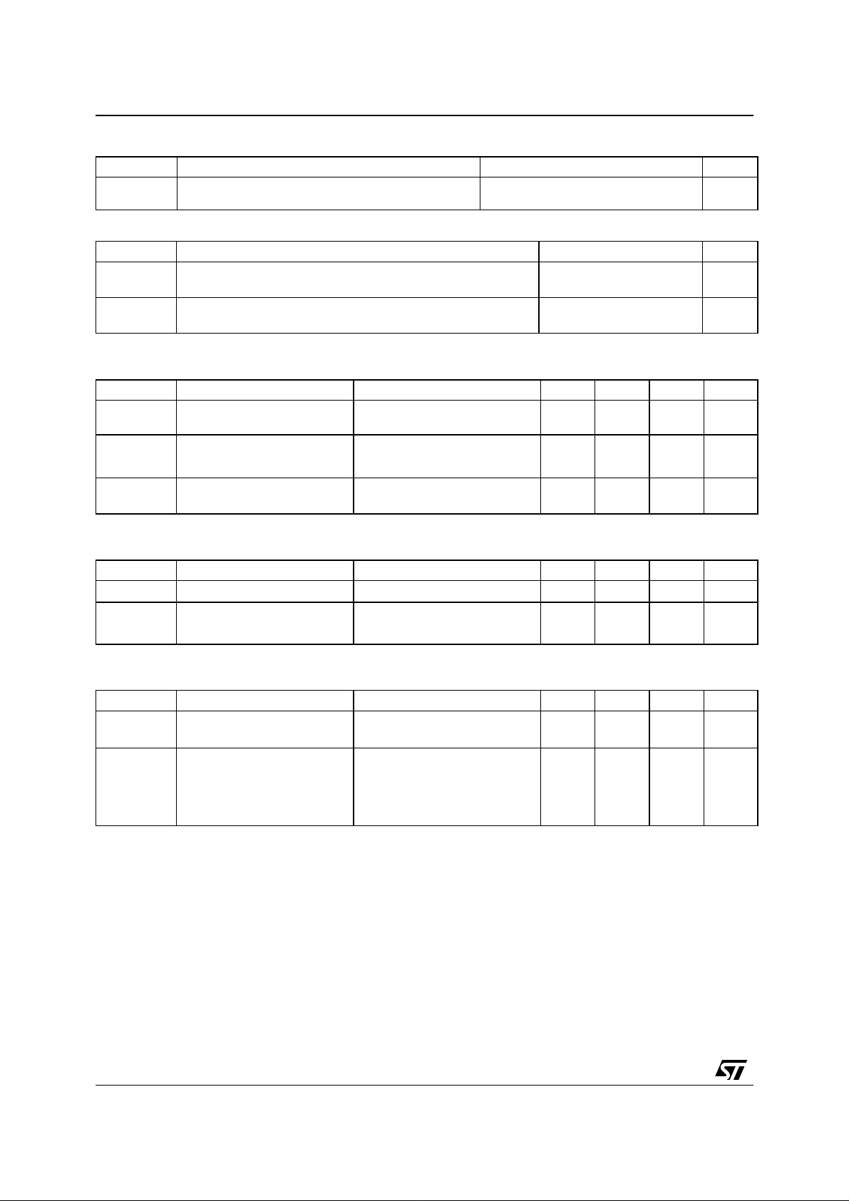
INTERNAL SCHEMATIC DIAGRAM
ABSOLUTE MAXIMUM RATINGS
Symbol Parameter Value Unit
V
DS
V
DGR
V
GS
I
D
I
D
I
DM
P
TOT
dv/dt (1) Peak Diode Recovery voltage slope 3 V/ns
V
ISO
T
stg
T
j
(•)Pu l se width limited by safe operati ng area
Drain-source Voltage (VGS = 0)
Drain-gate Voltage (RGS = 20 kΩ)
Gate- source Voltage ±30 V
Drain Current (continuos) at TC = 25°C
Drain Current (continuos) at TC = 100°C
(l)
Drain Current (pulsed) 212 A
Total Dissipation at TC = 25°C
Derating Factor 3.68 W/°C
Insulation Winthstand Voltage (AC-RMS) 2500 V
Storage Temperature – 65 to 150 °C
Max. Operating Junction Temperature 150 °C
(1) ISD≤ 53A, di/dt≤1 00 A /µ s, VDD≤ 24V, Tj≤ T
500 V
500 V
53 A
33 A
460 W
jMAX
1/8May 2002
Page 2
STE53NC50
THERMA L D ATA
Rthj-case Thermal Resistance Junction-case Max 0.272 °C/W
Rthc-h Thermal Resistance Case-heatsink with Conduct ive
Grease Applied
AVALANCHE CHARACTERISTICS
Symbol Parameter Max Value Unit
I
AR
E
AS
Avalanche Current, Repetitive or Not-Repetitive
(pulse width limited by T
max)
j
Single Pulse Avalanche Energy
(starting T
= 25 °C, ID = IAR, VDD = 50 V)
j
ELECTRICAL CHARACTERISTICS (TCASE = 25 °C UNLESS OTHERWISE SPECIFIED)
OFF
Symbol Parameter Test Conditions Min. Typ. Max. Unit
V
(BR)DSS
I
DSS
I
GSS
Drain-source
Breakdown Voltage
Zero Gate Voltage
Drain Current (V
GS
Gate-body Leakage
Current (V
DS
= 0)
= 0)
ID = 250 µA, VGS = 0 500 V
V
= Max Rating
DS
VDS = Max Rating, TC = 125 °C
V
= ± 30V ±100 nA
GS
0.05 °C/W
53 A
1043 mJ
10 µA
100 µA
ON
(1)
Symbol Parameter Test Conditions Min. Typ. Max. Unit
V
V
GS(th)
R
DS(on)
Gate Threshold Voltage
Static Drain-source On
= VGS, ID = 250µA
DS
VGS = 10V, ID = 27A
234V
0.07 0.08 Ω
Resistance
DYNAMIC
Symbol Parameter Test Conditions Min. Typ. Max. Unit
(1) Forward Transconductance VDS > I
g
fs
ID= 15 A
C
iss
C
oss
C
rss
Input Capacitance
Output Capacitance 1350 pF
Reverse Transfer
V
Capacitance
Note: 1. Pulsed: Pu l se duration = 300 µs, duty cycle 1. 5 %.
DS
D(on)
x R
DS(on)max,
= 25V, f = 1 MHz, VGS = 0
42 S
11.2 nF
115 pF
2/8
Page 3
STE53NC50
ELECTRICAL CHARACTERISTICS (CONTINUED)
SWITCHING ON
Symbol Parameter Test Conditions Min. Typ. Max. Unit
V
t
d(on)
Q
Q
Q
t
r
gs
gd
Turn-on Delay Time
Rise Time 70 ns
Total Gate Charge
g
Gate-Source Charge 46 nC
Gate-Drain Charge 150 nC
SWITCHING OFF
Symbol Param eter Test Conditions Min. Typ. Max. U nit
t
r(Voff)
t
t
f
c
Off-voltage Rise Time
Fall Time 38 ns
Cross-over Time 85 ns
SOURCE DRAIN DIODE
Symbol Parameter Test Conditions Min. Typ. Max. Unit
I
SD
I
SDM
VSD (1)
t
rr
Q
rr
I
RRM
Note: 1. Pulsed: Pulse duration = 300 µs, duty cycle 1.5 %.
2. Pulse width limi ted by safe operating area.
(2)
Source-drain Current 53 A
Source-drain Current (pulsed) 212 A
Forward On Voltage
Reverse Recovery Time
Reverse Recovery Charg e 17.86 µC
Reverse Recovery Curren t 47 A
= 250V, ID = 26.5A
DD
RG= 4.7Ω VGS = 10V
(see test circuit, Figure 3)
V
= 400V, ID = 53A,
DD
V
= 10V
GS
V
= 400V, ID = 53A,
DD
RG= 4.7Ω, V
GS
= 10V
(see test circuit, Figure 5)
ISD = 53A, VGS = 0
I
= 53A, di/dt = 100A/µs,
SD
V
= 70V, Tj = 150°C
DD
(see test circuit, Figure 5)
46 ns
310 434 nC
45 ns
1.6 V
760 ns
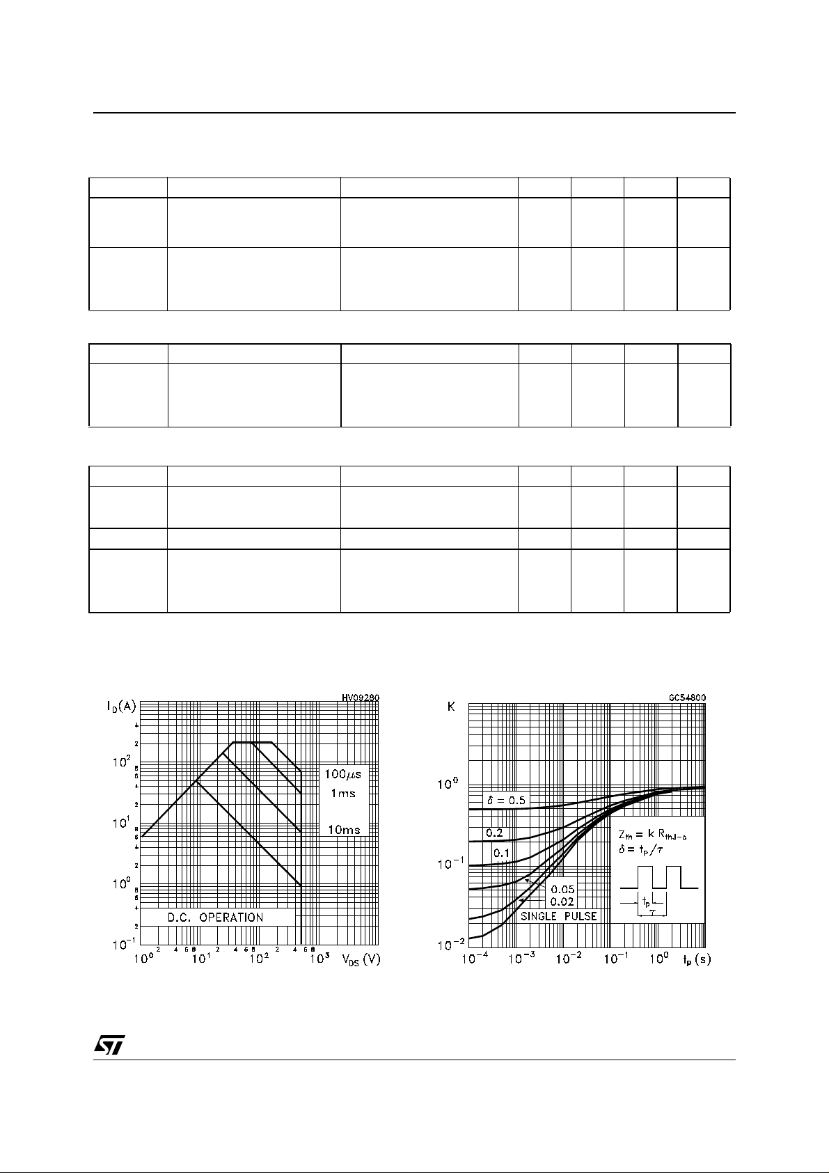
Safe Operating Area Thermal Impedence
3/8
Page 4

STE53NC50
Output Characteristics
Transconductance
Transfer Characteristics
Static Drain-source On Resistance
Gate Charge vs Gate-source Voltage
4/8
Capacitance Variations
Page 5

Source-drain Diode Forward Characteristics
STE53NC50
Normalized On Resistance vs TemperatureNormalized Gate Thereshold Voltage vs Temp.
5/8
Page 6

STE53NC50
Fig. 2: Unclamped Inductive WaveformFig. 1: Unclamped Inductive Load Test Circuit
Fig. 3: Switching Times Test Circuit For
Resistive Load
Fig. 5: Test Circuit For Inductive Load Switching
And Diode Recovery Times
Fig. 4: Gate Charge test Circuit
6/8
Page 7

ISOTOP MECHANICAL DATA
STE53NC50
DIM.
MIN. TYP. MAX. MIN. TYP. MAX.
A 11.8 12.2 0.466 0.480
B 8.9 9.1 0.350 0.358
C 1.95 2.05 0.076 0.080
D 0.75 0.85 0.029 0.033
E 12.6 12.8 0.496 0.503
F 25.15 25.5 0.990 1.003
G 31.5 31.7 1.240 1.248
H4 0.157
J 4.1 4.3 0.161 0.169
K 14.9 15.1 0.586 0.594
L 30.1 30.3 1.185 1.193
M 37.8 38.2 1.488 1.503
N4 0.157
O 7.8 8.2 0.307 0.322
mm inch
G
A
N
O
B
D
E
F
H
J
C
K
L
M
7/8
Page 8

STE53NC50
Information furnished is believed to be accurate and reliable. However, STMicroelectronics assumes no responsibility f or the
consequences of use of su ch in formation nor for any in fringement of patents or other rights of third parties w hich may result from
its use. No license is granted by implication or otherwise under any patent or patent rights of STMicroelectronics. Specifications
mentioned in this publication are subject to change without notice. This publication supersedes and replaces all information
previously suppli ed. STMi croelect ronics pr oducts are not author ized for use as cr itical component s in li fe suppo rt devi ces or
systems without express written approval of STMicroelectronics.
Australia - Brazil - Canada - China - Finland - France - Germany - Hong Kong - India - Israel - Italy - Japan - Malaysia - Malta - Morocco
© The ST logo is a registered trademark of STMicroelectronics
© 2002 STMicroelectronics - Printed in Italy - All Rights Reserved
Singapore - Spain - Sweden - Switzerland - United Kingdom - United States.
STMicroelectronics GROUP OF COMPANIES
© http://www.st.com
8/8
 Loading...