

Page 1
STE48NM50
N-CHANNEL 500V - 0.08Ω - 48A ISOTOP
MDmesh™Power MOSFET
TYPE V
STE48NM50 500V < 0.1Ω 48 A
n
TYPICAL RDS(on) = 0.08Ω
n
HIGH dv/dt AND AVALANCHE CAPABILITIES
n
100% AVALANCHE TESTED
n
LOW INPUT CAPACITANCE AND GATE
DSS
R
DS(on)
I
D
CHARGE
n
LOW GATE INPUT RESIST ANC E
n
TIGHT PROCESS CONTROL AND HIGH
MANUFACTURING YIELDS
DESCRIPTION
The MDmesh™
is a new revolutionary MOSFET
technology that associates the Multiple Drain process with the Company’s PowerMESH™ horizontal
layout. The resulting product has an outstanding low
on-resistance, impressively high dv/dt and excellent
avalanche characteristics. The adoption of the
Company’s proprietary strip technique yields overall
dynamic performance that is significantly better than
that of similar competition’s products.
APPLICATIONS
The MDmesh™ family is very suitable for increasing
power density of high voltage converters allowing
system miniaturization and higher efficiencies.
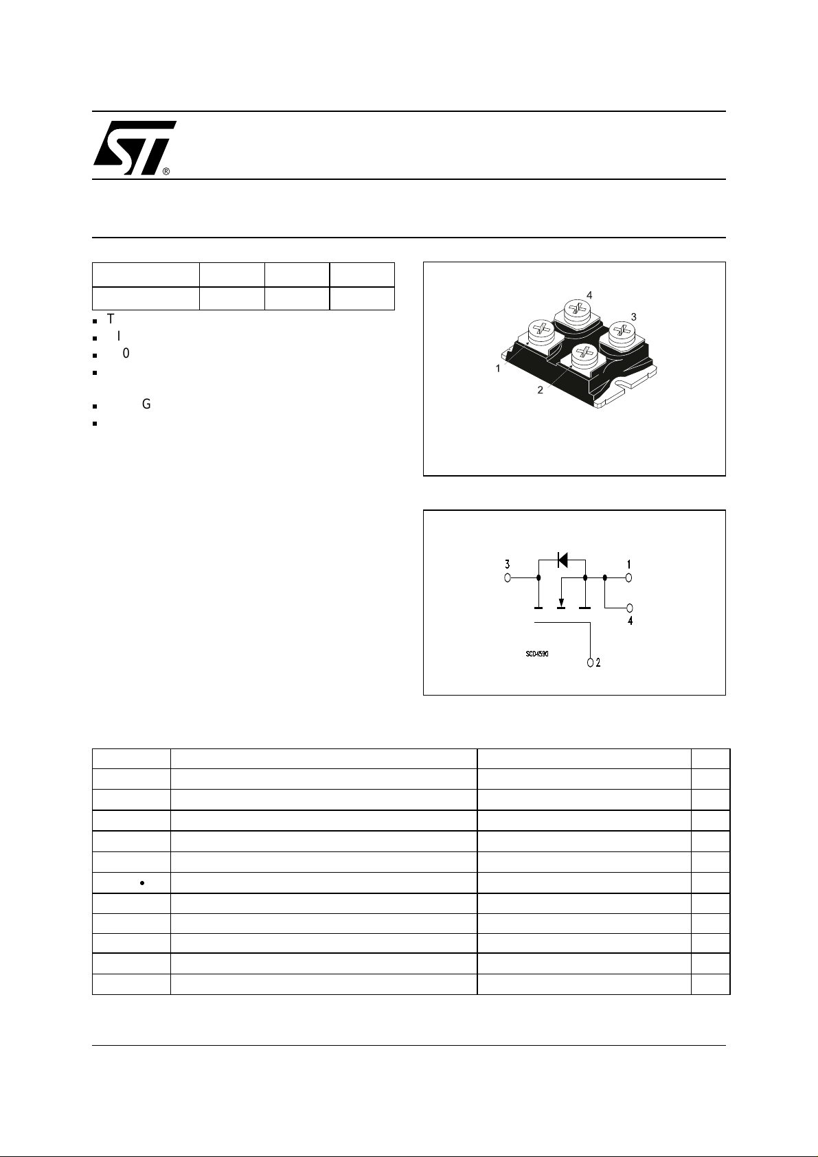
ISOTOP
INTERNAL SCHEMATIC DIAGRAM
ABSOLUTE MAXIMUM RATINGS
Symbol Parameter Value Unit
V
DS
V
DGR
V
GS
I
D
I
D
I
DM
P
TOT
dv/dt (1) Peak Diode Recovery voltage slope 15 V/ns
T
stg
T
j
(•)Pu l se width limited by safe operating area
Drain-source Voltage (VGS = 0)
Drain-gate Voltage (RGS = 20 kΩ)
Gate- source Voltage ±30 V
Drain Current (continuous) at TC = 25°C
Drain Current (continuous) at TC = 100°C
(l)
Drain Current (pulsed) 192 A
Total Dissipation at TC = 25°C
Derating Factor 3.6 W/°C
Storage Temperature –65 to 150 °C
Max. Operating Junction Temperature 150 °C
(1) ISD ≤48A, di/dt ≤400A/µs, VDD ≤ V
500 V
500 V
48 A
30 A
450 W
, Tj ≤ T
(BR)DSS
JMAX.
1/8September 2002
Page 2
STE48NM50
THERMA L D ATA
Rthj-case Thermal Resistance Junction-case Max 0.28 °C/W
Rthc-sink (*) Thermal Resistance Case-sink Typ 0.05 °C/W
(*) with conductive GREASE Appli e s
AVALANCHE CHARACTERISTICS
Symbol Parameter Max Value Unit
I
AR
E
AS
Avalanche Current, Repetitive or Not-Repetitive
(pulse width limited by T
max)
j
Single Pulse Avalanche Energy
(starting T
= 25 °C, ID = IAR, VDD = 50 V)
j
15 A
810 mJ
ELECTRICAL CHARACTERISTICS (T
= 25 °C UNLESS OTHERWISE SPECIFIED)
CASE
OFF
Symbol Parameter Test Conditions Min. Typ. Max. Unit
V
(BR)DSS
Drain-source
ID = 250 µA, VGS = 0 500 V
Breakdown Voltage
V
= Max Rating
DS
VDS = Max Rating, TC = 125 °C
V
= ± 30V ±100 nA
GS
10 µA
100 µA
ON
I
I
GSS
(1)
DSS
Zero Gate Voltage
Drain Current (V
GS
Gate-body Leakage
Current (V
DS
= 0)
= 0)
Symbol Parameter Test Conditions Min. Typ. Max. Unit
V
V
GS(th)
R
DS(on)
Gate Threshold Voltage
Static Drain-source On
= VGS, ID = 250µA
DS
VGS = 10V, ID = 24A
345V
0.08 0.1 Ω
Resistance
DYNAMIC
Symbol Parameter Test Conditions Min. Typ. Max. Unit
(1) Forward Transconductance VDS > I
g
fs
ID= 24A
C
iss
C
oss
C
rss
Input Capacitance
Output Capacitance 610 pF
Reverse Transfer
V
Capacitance
R
G
Gate Input Resistance f=1 MHz Gate DC Bias = 0
Test Signal Level = 20mV
Open Drain
Note: 1. Pulsed: Pu l se duration = 300 µs, duty c ycle 1.5 %.
DS
D(on)
x R
DS(on)max,
= 25V, f = 1 MHz, VGS = 0
20 S
3700 pF
50 pF
1.7 Ω
2/8
Page 3
STE48NM50
ELECTRICAL CHARACTERISTICS (CONTINUED)
SWITCHING ON
Symbol Parameter Test Conditions Min. Typ. Max. Unit
V
t
d(on)
Q
Q
Q
t
r
g
gs
gd
Turn-on Delay Time
Rise Time 35 ns
Total Gate Charge
Gate-Source Charge 23 nC
Gate-Drain Charge 42 nC
SWITCHING OFF
Symbol Param eter Test Conditions Min. Typ. Max. Unit
t
r(Voff)
t
t
f
c
Off-voltage Rise Time
Fall Time 23 ns
Cross-over Time 44 ns
SOURCE DRAIN DIODE
Symbol Parameter Test Conditions Min. Typ. Max. Unit
I
SD
I
SDM
VSD (1)
t
rr
Q
rr
I
rrm
t
rr
Q
rr
I
rrm
Note: 1. Pulsed: Pulse duration = 300 µs, duty cycle 1.5 %.
2. Pulse width limi ted by safe operating area.
(2)
Source-drain Current 48 A
Source-drain Current (pulsed) 192 A
Forward On Voltage
Reverse Recovery Time
Reverse Recovery Charg e
Reverse Recovery Curren t
Reverse Recovery Time
Reverse Recovery Charg e
Reverse Recovery Curren t
= 250V, ID = 24 A
DD
RG= 4.7Ω VGS = 10 V
(see test circuit, Figure 3)
V
= 400 V, ID = 48 A,
DD
V
= 10 V
GS
V
= 400 V, ID = 48 A,
DD
RG= 4.7Ω, V
GS
= 10 V
(see test circuit, Figure 5)
ISD = 48 A, VGS = 0
= 40 A, di/dt = 100A/µs,
I
SD
V
= 100 V, Tj = 25°C
DD
(see test circuit, Figure 5)
= 40 A, di/dt = 100A/µs,
I
SD
VDD = 100 V, Tj = 150°C
(see test circuit, Figure 5)
40 ns
87 117 nC
18 ns
1.5 V
520
7.8
30
680
11.2
33
ns
µC
A
ns
µC
A
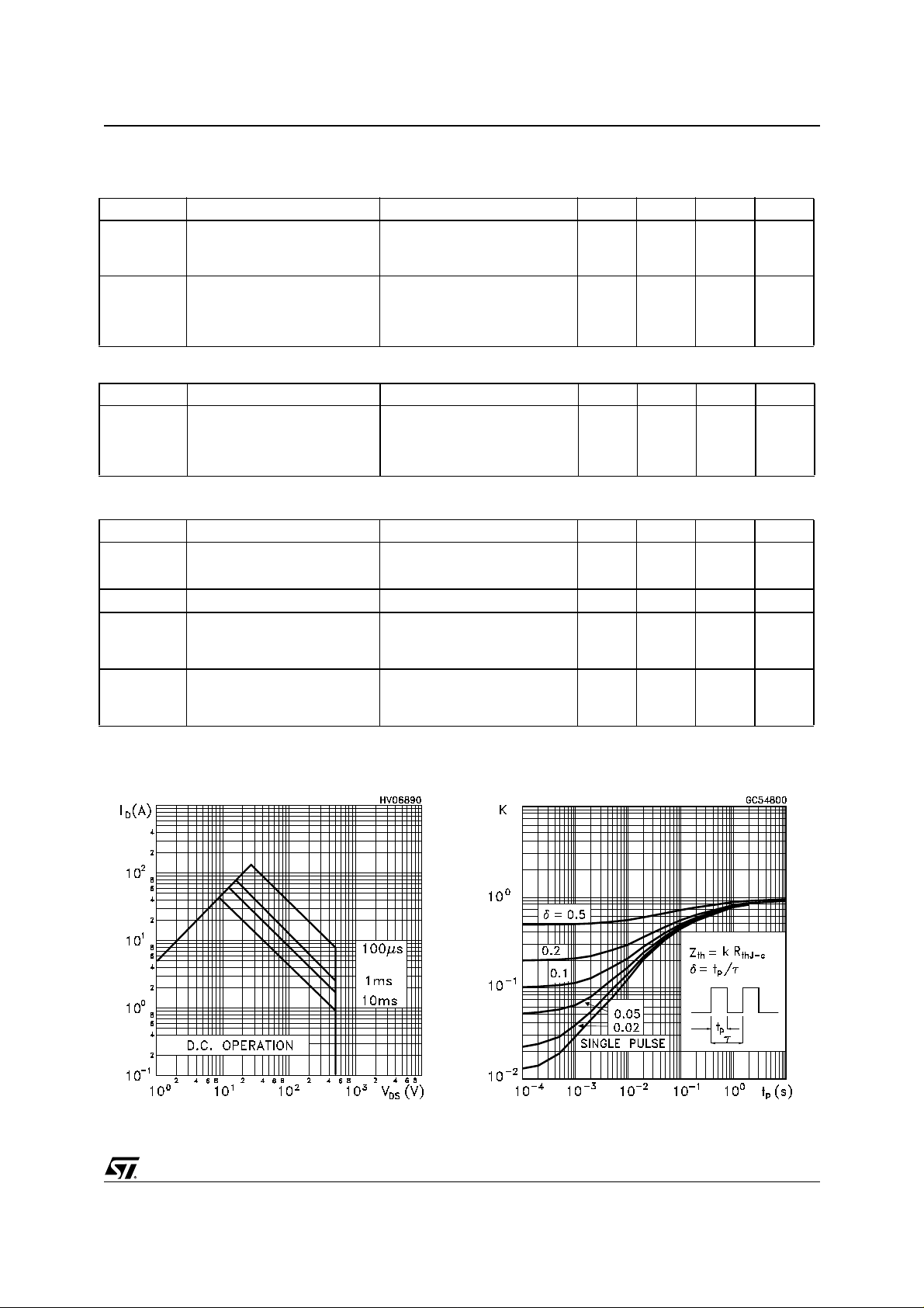
Thermal ImpedenceSafe Operating Area
3/8
Page 4

STE48NM50
Output Characteristics Transfer Characteristics
Transconductance Static Drain-source On Resistance
Gate Charge vs Gate-source Voltage Capacitance Variations
4/8
Page 5

Source-drain Diode Forward Characteristics
STE48NM50
Normalized On Resistance vs TemperatureNormalized Gate Thereshold Voltage vs Temp.
5/8
Page 6

STE48NM50
Fig. 2: Unclamped Inductive WaveformFig. 1: Unclamped Inductive Load Test Circuit
Fig. 3: Switching Times Test Circuit For
Resistive Load
Fig. 5: Test Circuit For Inductive Load Switching
And Diode Recovery Times
Fig. 4: Gate Charge test Circuit
6/8
Page 7

ISOTOP MECHANICAL DATA
STE48NM50
DIM.
MIN. TYP. MAX. MIN. TYP. MAX.
A 11.8 12.2 0.466 0.480
B 8.9 9.1 0.350 0.358
C 1.95 2.05 0.076 0.080
D 0.75 0.85 0.029 0.033
E 12.6 12.8 0.496 0.503
F 25.15 25.5 0.990 1.003
G 31.5 31.7 1.240 1.248
H4 0.157
J 4.1 4.3 0.161 0.169
K 14.9 15.1 0.586 0.594
L 30.1 30.3 1.185 1.193
M 37.8 38.2 1.488 1.503
N4 0.157
O 7.8 8.2 0.307 0.322
mm inch
G
A
N
O
B
D
E
F
H
J
C
K
L
M
7/8
Page 8

STE48NM50
Information furnished is believed to be accurate and reliable. However, STMicroelectronics assumes no responsibility f or the
consequences of use of su ch in formation nor for any in fringement of patents or other rights of third parties w hich may result from
its use. No license is granted by implication or otherwise under any patent or patent rights of STMicroelectronics. Specifications
mentioned in this publication are subject to change without notice. This publication supersedes and replaces all information
previously suppli ed. STMi croelect ronics pr oducts are not author ized for use as cr itical component s in li fe suppo rt devi ces or
systems without express written approval of STMicroelectronics.
Australia - Brazil - Canada - China - Finland - France - Germany - Hong Kong - India - Israel - Italy - Japan - Malaysia - Malta - Morocco
© The ST logo is a registered trademark of STMicroelectronics
© 2002 STMicroelectronics - Printed in Italy - All Rights Reserved
Singapore - Spain - Sweden - Switzerland - United Kingdom - United States.
STMicroelectronics GROUP OF COMPANIES
© http://www.st.com
8/8
 Loading...