

Page 1

查询STE26N50供应商
POWER MOS TRANSISTOR IN ISOTOP PACKAGE
STE26N50
N - CHANNEL ENHANCEMENT MODE
TYPE V
DSS
R
DS(on)
I
D
STE26N50 500 V < 0.2 Ω 26 A
■ HIGH CURRENT POWER MODULE
■ AVALANCHE RUGGED TECHNOLOGY
(SEE IRFP450 FOR RATING)
■ VERY LARGE SOA- LARGE PEAK POWER
CAPABILITY
■ EASY TO MOUNT
■ SAME CURRENT CAPABILITY FOR THE
TWO SOURCE TERMINALS
■ EXTREMELY LOW R
■ VERY LOW DRAIN TO CASE CAPACITANCE
■ VERY LOW INTERNAL PARASITIC
JUNCTION TO CASE
th
INDUCTANCE (TYPICALLY < 5 nH)
■ ISOLATED PACKAGE UL RECOGNIZED
(FILE No E81743)
INDUSTRIAL APPLICATIONS:
■ SMPS & UPS
■ MOTOR CONTROL
■ WELDING EQUIPMENT
■ OUTPUT STAGE FOR PWM, ULTRASONIC
CIRCUITS
4
3
1
2
ISOTOP
INTERNAL SCHEMATIC DIAGRAM
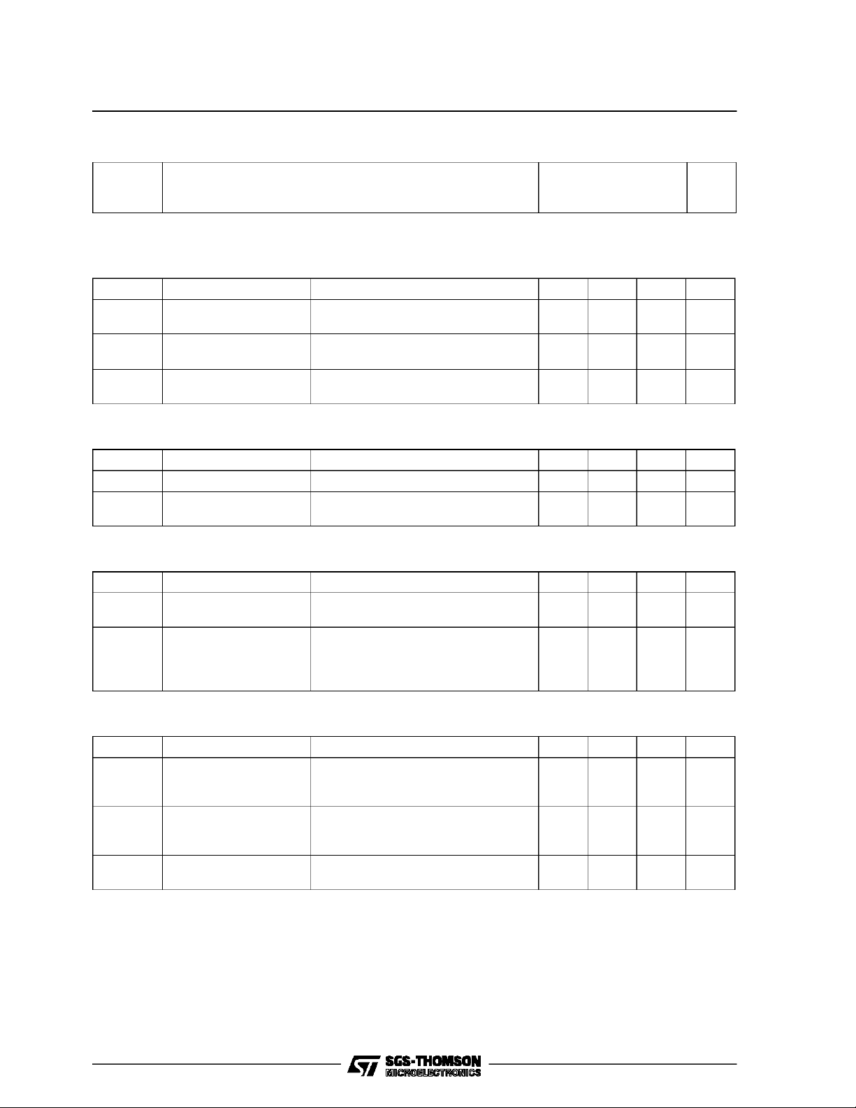
ABSOLUTE MAXIMUM RATINGS
Symb o l Paramet er Val u e Unit
V
V
V
I
DM
P
T
V
(•) Pulse widthlimitedbysafeoperating area
July 1993
Drain-Source Voltage (VGS= 0) 500 V
DS
Drain-Gate Voltage (RGS=20kΩ) 500 V
DGR
Gat e- Source Volta ge ± 20 V
GS
Drain Cur rent ( c ontinuous) at Tc=25oC26A
I
D
Drain Cur rent ( c ontinuous) at Tc=100oC17A
I
D
(•) Drain Curr ent ( pulsed) 104 A
Total Dissipation at Tc=25oC 300 W
tot
Derat ing Fac t or 2.4 W/
St or a ge Temperature -55 to 150
stg
Max. O per ating Junct ion Tem p era tur e 150
T
j
Ins ulation W it hstand Volt ag e (AC- RMS) 2500 V
ISO
o
C
o
C
o
C
1/8
Page 2
STE26N50
THERMAL DATA
R
thj-case
R
thc-h
Thermal Resistance Junction -c as e Max
Thermal Resistance Case- heatsi nk W ith Conductive
Gre ase Appli ed Max
0.42
0.05
o
C/W
o
C/W
ELECTRICAL CHARACTERISTICS (T
=25oC unless otherwise specified)
case
OFF
Symbol Parameter Test Condi tions Min. Typ. M ax. Unit
V
(BR)DSS
Drain - s ource
ID=1mA VGS= 0 V 500 V
Break d own Volt a ge
I
DSS
I
GSS
Zer o Gate Voltage
Drain Curr ent ( VGS=0)
Gat e- body Leakage
VDS=MaxRating
VDS= Max Rating x 0.8 Tc=125oC
200
1
VGS= ± 20 V ± 200 nA
Current (VDS=0)
ON (∗)
Symbol Parameter Test Condi tions Min. Typ. M ax. Unit
V
GS(th)
R
DS(on)
Gate T hreshold Voltage VDS=VGSID=1mA 2 4 V
St at ic Drain-sourc e On
VGS=10V ID=13A 0.2 Ω
Resistance
DYNAMIC
Symbol Parameter Test Condi tions Min. Typ. M ax. Unit
(∗)Forward
g
fs
Tr anscondu c t anc e
C
C
C
Input Capacitance
iss
Out put Capac itance
oss
Reverse Transfer
rss
Capacitance
VDS=15V ID=13A 12 S
VDS=25V f=1MHz VGS=0V 6
1200
500
µA
mA
nF
pF
pF
SWITCHING ON
Symbol Parameter Test Condi tions Min. Typ. M ax. Unit
2/8
t
d(on)
t
(di/dt)
Q
Turn-on Time
Rise Time
r
Turn-on Current S lope VDD= 400 V ID=26A
on
Total Gate Charge VDD= 400 V ID=26A
g
VDD=250V ID=13A
RG=4.7Ω VGS=10V
(see test circuit, figure 1)
R
=4.7Ω VGS=10V
G
(see test circuit, figure 3)
VGS=10V
60
80
450 A/µs
275 nC
ns
ns
Page 3

STE26N50
ELECTRICAL CHARACTERISTICS (continued)
SWITCHING OFF
Symbol Parameter Test Condi tions Min. Typ. M ax. Unit
t
r(Voff)
t
Off -voltage Rise T ime
t
Fall Time
f
Cross-over Time
c
SOURCE DRAIN DIODE
Symbol Parameter Test Condi tions Min. Typ. M ax. Unit
I
SD
I
SDM
V
SD
t
Q
I
RRM
(∗) Pulsed: Pulseduration= 300µs, dutycycle 1.5%
(•) Pulse width limited by safeoperatingarea
Source-drain Current
(•)
Source-drain Current
(pulsed)
(∗) Forward On Voltage ISD=26A VGS=0 1.4 V
Reverse Recov er y
rr
Time
Reverse Recov er y
rr
Charge
Reverse Recov er y
Current
VDD= 400 V ID=26A
RG=4.7Ω VGS=10V
(see test circuit, figure 3)
ISD=26A di/dt=100A/µs
VDD= 100 V Tj=150oC
(see test circuit, figure 3)
63
25
85
26
104
850
23.5
55
ns
ns
ns
A
A
ns
µC
A
Safe Operating Area Thermal Impedance
3/8
Page 4

STE26N50
Derating Curve
Transfer Characteristics
Output Characteristics
Transconductance
Static Drain-source On Resistance
4/8
Gate Charge vs Gate-source Voltage
Page 5

STE26N50
Capacitance Variations Normalized Gate Threshold Voltage vs
Temperature
Normalized Breakdown Voltage vsTemperature Normalized On Resistance vs Temperature
Turn-off Drain-source Voltage SlopeTurn-on Current Slope
5/8
Page 6

STE26N50
Cross-over Time Source-drain Diode Forward Characteristics
Fig. 1: Switching Times Test Circuits For
Resistive Load
Fig. 3: Test Circuit For Inductive Load Switching
And Diode Recovery Times
Fig. 2: Gate Charge Test Circuit
6/8
Page 7

ISOTOP MECHANICAL DATA
STE26N50
DIM.
MIN. TYP. MAX. MIN. TYP. MAX.
A 11.8 12.2 0.466 0.480
B 8.9 9.1 0.350 0.358
C 1.95 2.05 0.076 0.080
D 0.75 0.85 0.029 0.033
E 12.6 12.8 0.496 0.503
F 25.15 25.5 0.990 1.003
G 31.5 31.7 1.240 1.248
H 4 0.157
J 4.1 4.3 0.161 0.169
K 14.9 15.1 0.586 0.594
L 30.1 30.3 1.185 1.193
M 37.8 38.2 1.488 1.503
N 4 0.157
O 7.8 8.2 0.307 0.322
P 5.5 0.216
mm inch
G
O
A
B
N
D
E
F
H
J
C
K
L
M
0041565
7/8
Page 8

STE26N50
Information furnished is believed to be accurate and reliable. However, SGS-THOMSON Microelectronics assumes no responsability for the
consequences of useofsuchinformation nor for any infringement ofpatents orother rightsofthirdpartieswhich mayresults from itsuse. No
license isgranted by implicationorotherwise underany patent or patentrights of SGS-THOMSONMicroelectronics. Specificationsmentioned
in this publication are subjectto changewithout notice. Thispublicationsupersedesandreplaces all information previously supplied.
SGS-THOMSON Microelectronicsproducts arenotauthorizedfor use ascritical componentsin lifesupportdevices orsystemswithoutexpress
written approvalof SGS-THOMSONMicroelectonics.
1994 SGS-THOMSON Microelectronics- All RightsReserved
Australia - Brazil - France - Germany - Hong Kong - Italy -Japan- Korea -Malaysia- Malta - Morocco -The Netherlands-
Singapore - Spain - Sweden- Switzerland -Taiwan - Thailand - United Kingdom - U.S.A
SGS-THOMSON MicroelectronicsGROUP OF COMPANIES
8/8
 Loading...