

Page 1

查询STE250NS10供应商
STE250NS10
N-CHANNEL 100V - 0.0045 Ω - 220A ISOTOP
STripFET™ POWER MOSFET
TYPE
V
DSS
STE250NS10 100 V <0.0055
■ TYPICAL R
■ STANDARD THRESHOLD DRIVE
■ 100% AVALANCHE TESTED
(on) = 0.0045Ω
DS
R
DS(on)
I
D
220A
Ω
APPLICATIONS
■ SMPS & UPS
■ MOTOR CONTROL
■ WELDING EQUIPMENT
■ OUTPUT STAGE FOR PWM, ULTRASONIC
CIRCUITS
ISOTOP
INTERNAL SCHEMATIC DIAGRAM
ABSOLUTE MAXIMUM RATINGS
Symbol Parameter Value Unit
V
DS
V
DGR
V
GS
I
D
I
D
(
I
DM
P
tot
dv/dt
V
ISO
T
stg
T
j
(
Pulse width l i mited by safe operating area. (1 )ISD ≤220A, di/dt ≤200A/µs, VDD ≤ V
•)
.
Drain-source Voltage (VGS = 0)
Drain-gate Voltage (RGS = 20 kΩ)
100 V
100 V
Gate- source Voltage ± 20 V
Drain Current (continuos) at TC = 25°C
Drain Current (continuos) at TC = 100°C
•)
Drain Current (pulsed) 880 A
Total Dissipation at TC = 25°C
220 A
156 A
500 W
Derating Factor 4 W/°C
(1)
Peak Diode Recovery voltage slope 3.5 V/ns
Insulation Withstand Voltage (AC-RMS) 2500 V
Storage Temperature -55 to 150 °C
Operating Junction Temperature 150 °C
(BR)DSS
, Tj ≤ T
JMAX
.
1/8September 2001
Page 2

STE250NS10
THERMA L D ATA
Rthj-case
Rthj-amb
AVALANCHE CHARACTERISTICS
Symbol Parameter Max Value Unit
I
AR
E
AS
Thermal Resistance Junction-case
Thermal Resistance Junction-ambient
Avalanche Current, Repetitive or Not-Repetitive
(pulse width limited by T
max)
j
Single Pulse Avalanche Energy
(starting T
= 25 °C, ID = IAR, VDD = 64 V)
j
Max
Max
0.25
50
220 A
800 mJ
°C/W
°C/W
ELECTRICAL CHARACTERISTICS (T
= 25 °C unless otherwise specified)
case
OFF
Symbol Parameter Test Conditions Min. Typ. Max. Unit
V
(BR)DSS
Drain-source Breakdown
I
= 1 mA VGS = 0
D
100 V
Voltage
V
= Max Rating
DS
V
= Max Rating TC = 125°C
DS
= ± 20V
V
GS
50
500
±400 nA
ON
(*)
I
DSS
I
GSS
Zero Gate Voltage
Drain Current (V
GS
Gate-body Leakage
Current (V
DS
= 0)
= 0)
Symbol Parameter Test Conditions Min. Typ. Max. Unit
V
V
GS(th)
R
DS(on)
Gate Threshold Voltage
Static Drain-source On
Resistance
= VGS I
DS
V
= 10 V ID = 125 A
GS
= 250 µA
D
234V
0.0045 0.0055
DYNAMIC
Symbol Parameter Test Conditions Min. Typ. Max. Unit
V
g
fs
C
iss
C
oss
C
rss
Forward Transconductance
Input Capacitance
Output Capacitance
Reverse Transfer
Capacitance
= 20 V ID= 70 A
DS
= 25V, f = 1 MHz, VGS = 0
V
DS
60 S
31
4.3
1.2
µA
µA
Ω
nF
nF
nF
2/8
Page 3
STE250NS10
ELECTRICAL CHARACTERISTICS (continued)
SWITCHING ON
Symbol Parameter Test Conditions Min. Typ. Max. Unit
= 50 V ID = 125 A
t
d(on)
Turn-on Delay Time
t
r
Rise Time
V
DD
R
= 4.7 Ω VGS = 10 V
G
(Resistive Load, Figure 3)
Q
g
Q
gs
Q
gd
Total Gate Charge
Gate-Source Charge
Gate-Drain Charge
= 50V ID= 220A V
V
DD
GS
= 10V
SWITCHING OFF
Symbol Parameter Test Conditions Min. Typ. Max. Unit
= 50 V ID = 125 A
t
d(off)
Turn-off Delay Time
t
f
Fall Time
V
DD
R
= 4.7Ω, V
G
GS
= 10 V
(Resistive Load, Figure 3)
110
380
900
160
330
1100
330
ns
ns
nC
nC
nC
ns
ns
t
r(Voff)
t
t
f
c
Fall Time
Cross-over Time
Off-voltage Rise Time
= 80 V ID = 220 A
V
clamp
R
= 4.7Ω, V
G
GS
= 10 V
(Inductive Load, Figure 5)
950
330
600
SOURCE DRAIN DIODE
Symbol Parameter Test Conditions Min. Typ. Max. Unit
I
SD
I
SDM
V
SD
t
rr
Q
rr
I
RRM
(*)
Pulsed: P ul se duration = 300 µs, duty cycle 1.5 %.
(
•)Pulse width limited by s afe operating area.
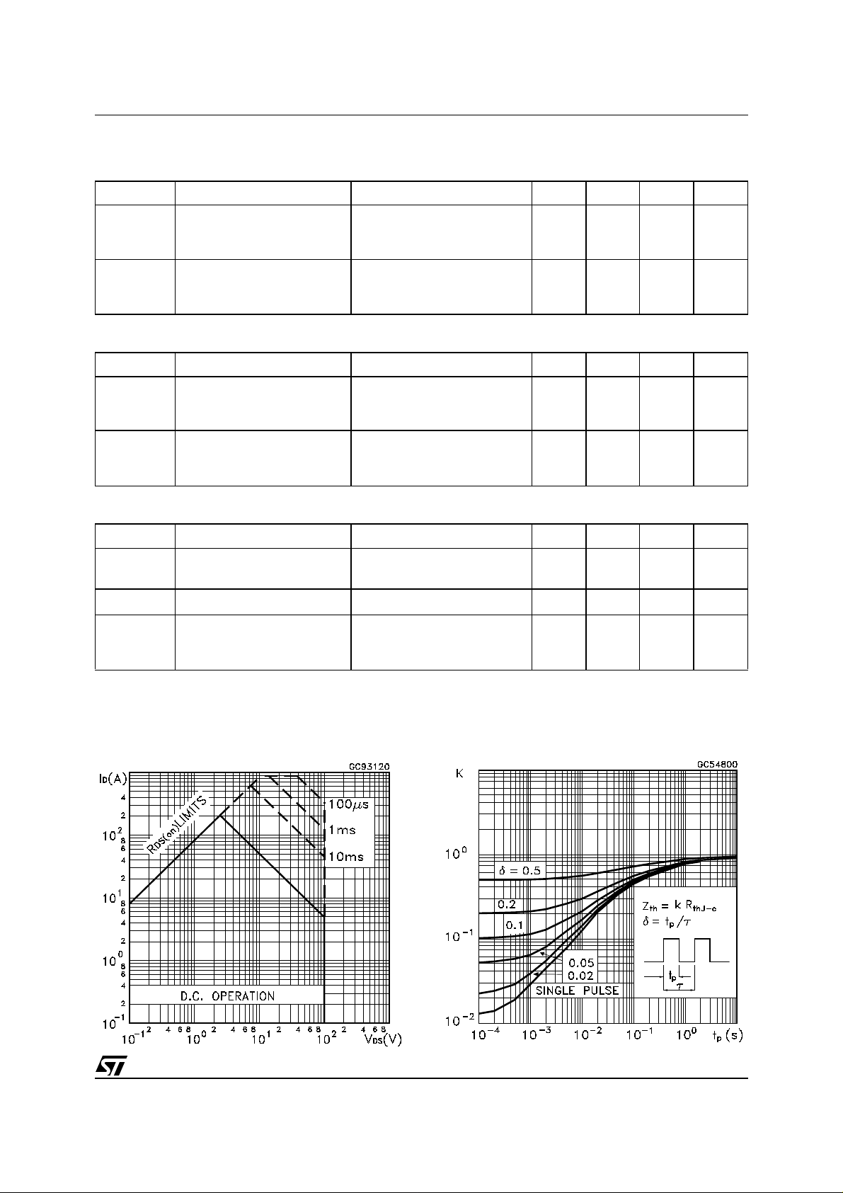
Safe Operating Area
Source-drain Current
(•)
Source-drain Current (pulsed)
(*)
Forward On Voltage
Reverse Recovery Time
Reverse Recovery Charge
Reverse Recovery Current
I
= 220 A VGS = 0
SD
= 220 A di/dt = 100A/µs
I
SD
V
= 30 V Tj = 150°C
DD
(see test circuit, Figure 5)
Thermal Impedance
220
880
1.5 V
200
1.35
13.5
ns
ns
ns
ns
µ
A
A
C
A
3/8
Page 4

STE250NS10
Output Characteristics Transfer Characteristics
Transconductance Static Drain-source On Resistance
Gate Charge vs Gate-source Voltage Capacitance Variations
4/8
Page 5

STE250NS10
Normalized Gate Threshold Voltage vs Temperature Normalized on Resistance vs Temperature
Source-drain Diode Forward Characteristics Normalized Breakdown Voltage vs Temperature.
. .
. .
5/8
Page 6

STE250NS10
Fig. 1: Unclamped Inductive Load Test CircuitFig. 1: Unclamped Inductive Load Test Circuit Fig. 2: Unclamped Inductive Waveform
Fig. 3: Switching Times Test Circuits For Resistive
Load
Fig. 5: Test Circuit For Inductive Load Switching
And Diode Recovery Times
Fig. 4: Gate Charge test Circuit
6/8
Page 7

ISOTOP MECHANICAL DATA
STE250NS10
DIM.
MIN. TYP. MAX. MIN. TYP. MAX.
A 11.8 12.2 0.466 0.480
B 8.9 9.1 0.350 0.358
C 1.95 2.05 0.076 0.080
D 0.75 0.85 0.029 0.033
E 12.6 12.8 0.496 0.503
F 25.15 25.5 0.990 1.003
G 31.5 31.7 1.240 1.248
H4 0.157
J 4.1 4.3 0.161 0.169
K 14.9 15.1 0.586 0.594
L 30.1 30.3 1.185 1.193
M 37.8 38.2 1.488 1.503
N4 0.157
O 7.8 8.2 0.307 0.322
mm inch
N
O
G
A
B
D
E
F
H
J
C
K
L
M
7/8
Page 8

STE250NS10
Information furnished is believed to be accurate and reliable. However, STMicroelectronics assumes no responsibility for the consequences
of use of such information nor for any infringement of patents or other rights of third parties which may result from its use. No license is granted
by implic ation or otherwise under any patent or patent r i ght s of STMi croelectr oni cs. Spec i fications mentione d i n this publicatio n are subj ect
to change without notice. This publication supersedes and replaces all information previously supplied. STMicroelectronics product s are not
authorized for use as cri tical comp onents in lif e support devi ces or systems without express written approva l of STMicroe l ectronics.
The ST logo is registered trademark of STMicroelectronics
2001 STMi croelectronics - All Ri ghts Rese rved
All other na m es are the property of their respective owners.
Australi a - Brazil - Ch i na - Finland - France - Germany - Hong K ong - India - Ita l y - Japan - Malaysia - Malt a - M orocco -
Singap ore - Spain - Sw eden - Switze rland - United Kingdom - U.S.A.
STMicroelectronics GROUP OF COMPANIES
http:// www.st.com
8/8
 Loading...