

Page 1
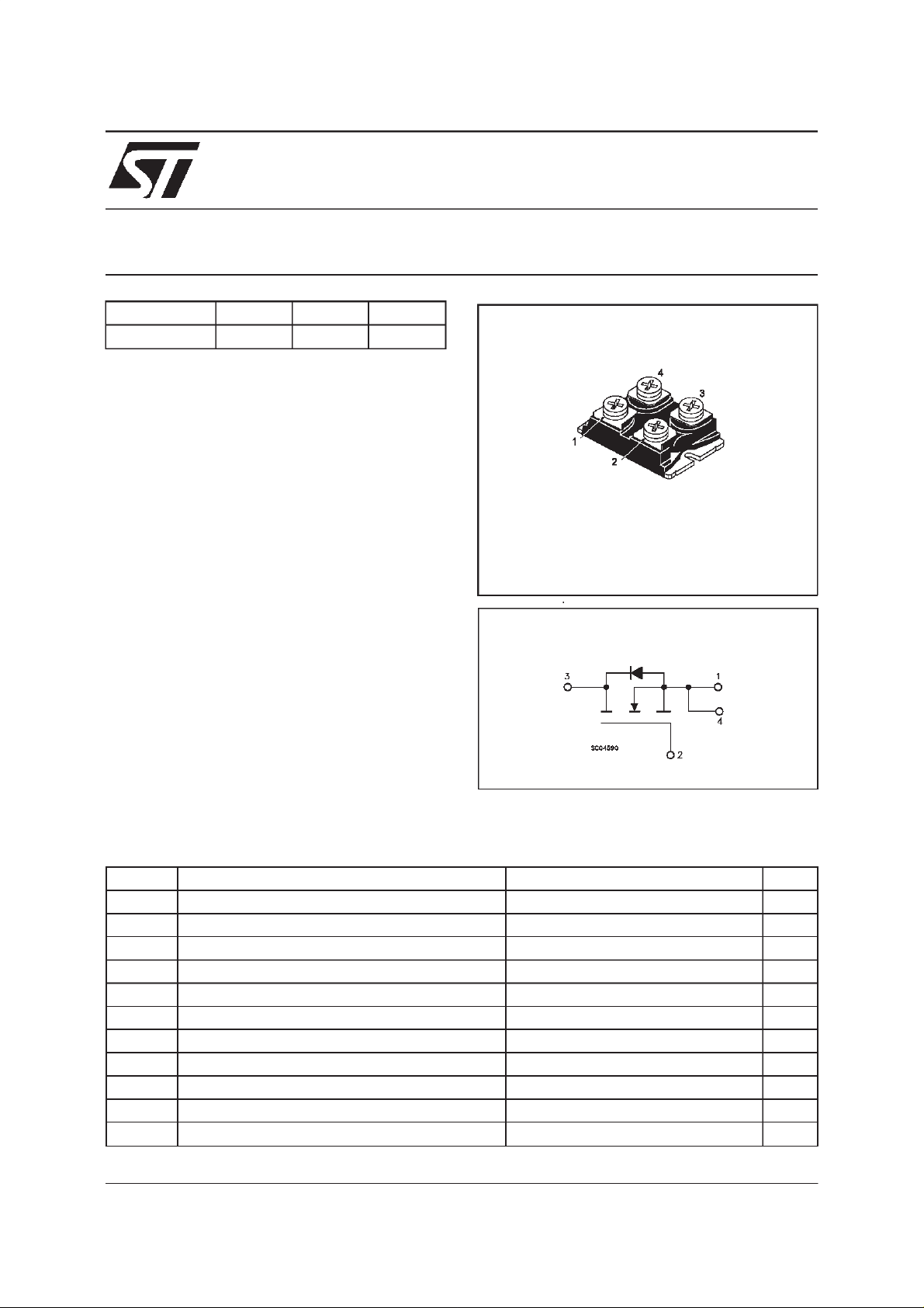
STE24NA100
N - CHANNEL 1000V - 0.35Ω - 24A - ISOTOP
FAST POWER MOSFET
TYPE V
DSS
R
DS(on)
I
D
ST E24NA100 1000 V < 0. 385 Ω 24 A
■ TYPICALR
30V GATE TO SOURCE VOLTAGERATING
■
±
■ 100%AVALANCHETESTED
■ LOW INTRINSICCAPACITANCE
■ GATECHARGE MINIMIZED
■ REDUCEDVOLTAGESPREAD
DS(on)
= 0.35 Ω
APPLICATIONS
■ HIGHCURRENT, HIGH SPEED SWITCHING
■ SWITCHMODE POWER SUPPLY (SMPS)
■ DC-AC CONVERTERFOR WELDING
EQUIPMENTANDUNINTERRUPTABLE
POWERSUPPLY AND MOTOR DRIVE
ISOTOP
INTERNAL SCHEMATIC DIAGRAM
ABSOLUTE MAXIMUM RATINGS
Symb o l Parameter Value Unit
V
V
V
I
DM
P
T
V
(•) Pulsewidth limited by safeoperating area
October 1998
Drain-source Voltage (VGS= 0) 1000 V
DS
Drain- g at e V olt ag e (RGS=20kΩ) 1000 V
DGR
Gate-s ource Voltage
GS
I
Drain Cur rent (cont inu ous ) at Tc=25oC24A
D
I
Drain Cur rent (cont inu ous ) at Tc=100oC15A
D
30 V
±
(•) Drain Cur rent (pulsed) 96 A
Tot al Dissi pat ion at Tc=25oC 450 W
tot
Derat ing F ac tor 3.6 W/
Sto rage Temperat ure -55 to 150
stg
T
Max. Operating J unction T emperat ure 150
j
Ins ulat i on Wi t hs t an d V olt ag e (AC- RMS) 2500 V
ISO
o
C
o
C
o
C
1/8
Page 2
STE24NA100
THERMAL DATA
R
thj-case
R
thc-h
AVALANCHE CHARACTERISTICS
Symbol Parameter Max Valu e Unit
I
AR
E
Ther mal Resistanc e Junct ion-case Max
Ther mal Resistanc e Case-heatsink Wit h C onductive
Gr ease Applied Max
Avalanche Current, Repetitive or Not-Repetitive
(pulse width limited by T
Single Pul se A v alan c he Ener gy
AS
(starting T
=25oC, ID=IAR,VDD=50V)
j
max)
j
0.27
0.05
12 A
2000 mJ
o
C/W
o
C/W
ELECTRICAL CHARACTERISTICS
=25oC unless otherwisespecified)
(T
case
OFF
Symbol Parameter Test Conditions Min. Typ. M ax. Unit
V
(BR)DSS
Drain-source
ID=500µAVGS= 0 1000 V
Break dow n Vo lt age
I
DSS
I
GSS
Zero Gate Voltage
Drain Curre nt (V
GS
Gat e- bod y Leakag e
Current (V
DS
=0)
=0)
V
=MaxRating
DS
=MaxRating Tc= 125oC
V
DS
= ± 30 V ± 400 nA
V
GS
50
250
ON(∗)
Symbol Parameter Test Conditions Min. Typ. M ax. Unit
V
GS(th)
R
DS(on)
Gate Threshold Voltage VDS=V
Sta t ic Drain-s our c e On
VGS=10V ID= 12 A 0.35 0 . 385 Ω
GS
ID=1mA 2.25 3 3.75 V
Resistance
I
D(on)
On State Drain Current VDS>I
D(on)xRDS(on )max
24 A
VGS=10V
DYNAMIC
Symbol Parameter Test Conditions Min. Typ. M ax. Unit
g
(∗)Forward
fs
Tr ansc on duc tance
C
C
C
Input Capacitanc e
iss
Out put Capac itance
oss
Reverse Transfer
rss
Capacit a nc e
VDS>I
D(on)xRDS(on )max
ID=12A 15 S
VDS=25V f=1MHz VGS=0 14000
1200
300
19000
1600
390
µA
µ
pF
pF
pF
A
2/8
Page 3
STE24NA100
ELECTRICAL CHARACTERISTICS
(continued)
SWITCHINGON
Symbol Parameter Test Conditions Min. Typ. M ax. Unit
t
d(on)
t
r
Turn-on Time
Rise T i m e
VDD=500V ID=12A
R
=4.7
G
Ω
VGS=10V
40
55
56
77
(see test circuit, figure 3)
Q
Q
Q
Tot al Gate Charge
g
Gat e- Source Char g e
gs
Gate-Drain Charge
gd
VDD= 800 V ID=24A VGS= 10 V 470
43
226
660 nC
SWITCHINGOFF
Symbol Parameter Test Conditions Min. Typ. M ax. Unit
t
r(Voff)
t
t
Off-volt age Rise Time
Fall T ime
f
Cross-over Tim e
c
VDD=800V ID=24A
=4.7 Ω VGS=10V
R
G
(see test circuit, figure 5)
110
25
150
154
35
210
SOURCEDRAINDIODE
Symbol Parameter Test Conditions Min. Typ. M ax. Unit
I
SDM
V
I
SD
Q
I
RRM
SD
t
Source-drain Current
(•)
Source-drain Current
24
96
(pulsed)
(∗)ForwardOnVoltage ISD=24A VGS=0 1.6 V
Reverse Recovery
rr
Time
Reverse Recovery
rr
ISD= 24 A di/dt = 100 A/µs
= 100 V Tj=150oC
V
DD
(see test circuit, figure 5)
1.4
41
Charge
Reverse Recovery
60
Current
ns
ns
nC
nC
ns
ns
ns
A
A
µ
µ
A
s
C
(∗) Pulsed:Pulse duration = 300µs, duty cycle 1.5%
(•) Pulse width limited by safeoperating area
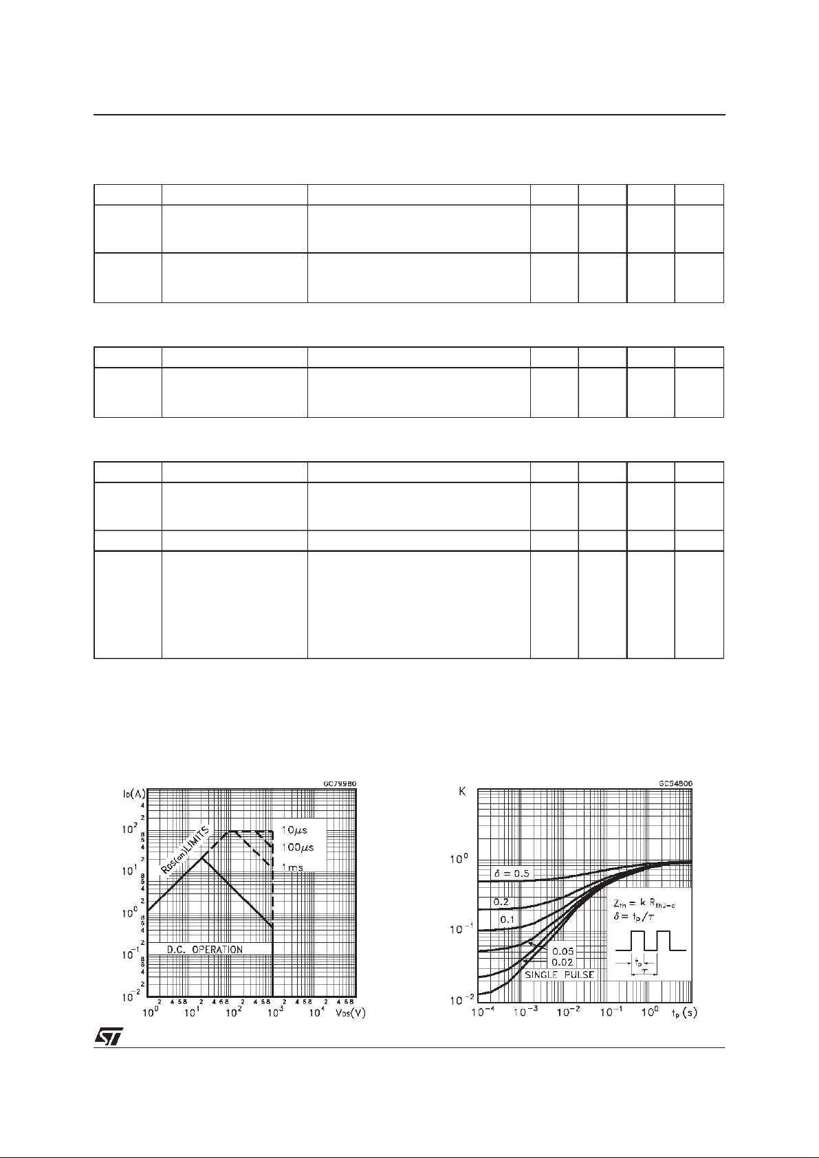
SafeOperating Area Thermal Impedance
3/8
Page 4

STE24NA100
OutputCharacteristics
Transconductance
TransferCharacteristics
Static Drain-sourceOn Resistance
Gate Charge vs Gate-sourceVoltage
4/8
CapacitanceVariations
Page 5

STE24NA100
NormalizedGate ThresholdVoltage vs
Temperature
Source-drainDiode Forward Characteristics
NormalizedOn Resistancevs Temperature
5/8
Page 6

STE24NA100
Fig. 1:
UnclampedInductiveLoad TestCircuit
Fig. 3: SwitchingTimes TestCircuits For
ResistiveLoad
Fig. 2:
UnclampedInductiveWaveform
Fig. 4: Gate Charge test Circuit
Fig. 5:
Test CircuitFor InductiveLoad Switching
And Diode Recovery Times
6/8
Page 7

ISOTOPMECHANICALDATA
STE24NA100
DIM.
MIN. TYP. MAX. MIN. TYP. MAX.
A 11.8 12.2 0.466 0.480
B 8.9 9.1 0.350 0.358
C 1.95 2.05 0.076 0.080
D 0.75 0.85 0.029 0.033
E 12.6 12.8 0.496 0.503
F 25.15 25.5 0.990 1.003
G 31.5 31.7 1.240 1.248
H 4 0.157
J 4.1 4.3 0.161 0.169
K 14.9 15.1 0.586 0.594
L 30.1 30.3 1.185 1.193
M 37.8 38.2 1.488 1.503
N 4 0.157
O 7.8 8.2 0.307 0.322
mm inch
G
A
B
O
N
D
E
F
H
J
C
K
L
M
7/8
Page 8

STE24NA100
Information furnished is believed to beaccurate and reliable. However, STMicroelectronics assumes no responsibility forthe consequences
of use of such information nor for any infringement of patents or other rights of third parties which may result from its use. No license is
granted by implication or otherwise under any patent or patentrights of STMicroelectronics. Specification mentioned in this publication are
subject to change withoutnotice. This publication supersedes and replaces all informationpreviously supplied. STMicroelectronics products
are not authorized for use as critical components in life support devices orsystems without express written approval of STMicroelectronics.
The ST logo is a trademark of STMicroelectronics
1998 STMicroelectronics – Printedin Italy – All Rights Reserved
STMicroelectronics GROUP OF COMPANIES
Australia - Brazil - Canada -China -France -Germany - Italy - Japan -Korea -Malaysia - Malta -Mexico - Morocco -The Netherlands -
Singapore - Spain - Sweden -Switzerland - Taiwan- Thailand - UnitedKingdom -U.S.A.
http://www.st.com
.
8/8
 Loading...