

Page 1
查询STE2004供应商
102 X 65 SINGLE CHIP LCD CONTROLLER / DRIVER
STE2004
■ 102 x 65 bits Display Data RAM
■ Programmable MUX rate
■ Programmable Frame Rate
■ X,Y Programmable Carriage Return
■ Dual Partial Display Mode
■ Row by Row Scrolling
■ Automatic data RAM Blanking procedure
■ Selectable Input Interface:
• I2C Bus Fast and Hs-mode (read and write)
• 68000 & 8080 Parallel Interf aces (read and write)
• 3-lines and 4-lines SPI Interface (read and write)
• 3-lines 9 bit Serial Interface (read and write)
■ Fully Integrated Oscillat or requires no ex ternal
components
■ CMOS Compatible Inputs
■ Fully Integrated Configurable LCD bias voltage
generator with:
• Selectabl e
multiplication factor (up to 5X)
• Effective sensing for High Precision Output
• Eight selectable temperature compensation
coefficients
■ Designed for chip-on-glass (COG) applications.
■ Low Power Consumption, suitable for battery
operated systems
■ Logic Supply Voltage range from 1.7 to 3.6V
■ High Voltage Generator Supply Voltage range
from 1.75 to 4.5V
■ Display Supply Voltage range from 4.5 to 14.5V
■ Backward Compatibility with STE2001 and
STE2002
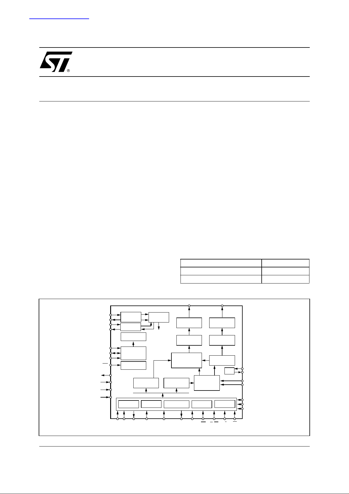
DESCRIPTION
The STE2004 is a low power CMOS LCD controller driver. Designed to drive a 65 rows by 102 columns graphic display, it provides all necessary
functions in a single chip, including on-chi p LCD
supply and bias voltages generators, resulting in a
minimum of externals compone nts and in a very
low power consumption.
STE2004 features six standard interfaces (3-lines
Serial, 3-lines SPI, 4-lines SPI, 68000 Parallel,
8080 parallel & I
2
C) for ease of interfacing with the
host micro-controller
Type Ordering Number
Bumped Wafers STE2004DIE1
Bumped Dice on Waffle Pack
STE2004DIE2
Figure 1. Block Diagram
OSC_IN
OSC_OUT
FR_IN
FR_OUT
VSENSE SLAVE
VLCD
VLCDSENSE
VSSAUX
VDD1,2
V
SS
SEL1,2
July 2003
RES
OSC
MASTER
SLAVE SYNC
BIAS VOLTAGE
GENERATOR
HIGH VOLTAGE
GENERATOR
RESET
I2C BUS
SAO SDIN/SDA_IN SDA_OUTSCLK/SCL
GENERATOR
DATA
REGISTER
9 Bit SERIAL
TIMING
CLOCK
INSTRUCTION
REGISTER
3 & 4 Line SPI
CO to C101 R0 to R64
COLUMN
DRIVERS
DATA
LATCHES
65 x 102
DRIVERS
REGISTER
SCROLL
RAM
DISPLAY
CONTROL
LOGIC
Parallel 8080
DB0
to
DB7
Parallel 68K
ROW
SHIFT
LOGIC
TEST
D/C CSSA1 SDOUT E/WR R/W- RD
TEST_MODE
TEST_VREF
ICON_MODE
EXT
SEL 0
SEL 1
SEL 2
LR0047
1/67
Page 2
STE2004
PIN DESCRIPTION
N° Pad Type Function
R0 to R64 1-6
109-141
C0 to C101 6-107 O LCD Column Driver Output
SS 192-203 GND Ground pads.
V
DD1 156-163 Supply IC Positive Power Supply
V
DD2 164-171 Supply Internal Generator Supply Voltages.
V
LCD 205-209 Supply Voltage Multiplier Output
V
V
LCDSENSE
V
SENSE_SLAVE
V
SSAUX
204 Supply
145 Supply Voltage reference f or SLAVE CHARGE PUMP
190-177-
147
V
DD1AUX
142 O VDD1 Reference for Pins Configuration
SEL1,2,3 152
153
154
O LCD Row Driver Output
V oltage Multiplier Regulation Input. V
O Ground Reference for Pins Configuration
I Interface Mode Selection
- CANNOT BE LEFT FLOATING
SEL3 SEL2 SEL1 Interface
GND / VSSAUX GND / VSSAUX GND / VSSA UX
GND / VSSAUX GND / VSSAUX VDD1
GND / VSSAUX VDD1 GND / VSSAUX
GND / VSSAUX VDD1 VDD1
VDD1 GND / VSSAUX GN D / VSSAUX
VDD1 GND / VSSA UX VDD1
Sensing for Output Voltage Fine Tuning
LCDOUT
SPI 4-Lines 8 bit
SPI 3-Lines 8 bit
Serial 3-Lines 9 bit
Parallel 8080-series
Parallel 68000-series
I2C
EXT_SET 151 I Extended Instruction Set Selection
- CANNOT BE LEFT FLOATING
EXT PAD CONFIG INSTRUCTION SET SELECTED
GND or VSSAUX BASIC
VDD1 EXTENDED
ICON_MODE
155 I Extended Instruction Set Selection
- CANNOT BE LEFT FLOATING
ICON MODE PAD CONFIG ICON MODE STATUS
GND or VSSAUX DISBLED
VDD1 ENABLED
SDOUT 180 O Serial & SPI Data Output - IF UNUSED MUST BE LEFT FLOATING
SDIN - SDAIN 179 I SDIN - Serial & SPI Interface Data Input - CANNOT BE LEFT FLOATING
I
SDA IN - I
2
C Bus Data In - CANNOT BE LEFT FLOATING
SCLK - SCL 181 I SCLK - Serial & SPI Interface Clock - CANNOT BE LEFT FLOATING
I
SDA_OUT 178 O
SA0 149 I
SA1 148 I
2
C bus Clock - CANNOT BE LEFT FLOATING
SCL - I
2
C Bus Data Out IF UNUSED MUST BE LEFT FLOATING
I
2
C Slave Address BIT 0 - CANNOT BE LEFT FLOATING
I
2
C Slave Address BIT 1- CANNOT BE LEFT FLOATING
I
DB0 to DB7 182-189 I/O Paral lel Interface 8 Bi t Da ta Bus - CANNOT BE LEFT FLOATING
- RD 175 I R/W - 68000 Series Parallel Interface Read & Write Control Input
R/W
- CANNOT BE LEFT FLOATING
IRD
- 8080 Series Parallel Interface Read enable Clock Input
- CANNOT BE LEFT FLOATING
E / WR
176 I E - 68000 Series Parallel Interface Read & Write Clock Input
- CANNOT BE LEFT FLOATING
2/67
Page 3
STE2004
PIN DESCRIPTION
N° Pad Type Function
E / WR 176 I WR - 8080 Series Parallel Interface - Write enable clock input
RES
D/C
CS
TEST_MODE 191 I Test Pad - 50 kohm internal Pull-down MUS T BE CO NNEC TED TO VSS/VS SAUX
TEST_VREF 146 O Test Pad - MUST B E LEF T FLOATIN G
OSCIN 144 I
OSCOUT 210 O Internal/External Oscillator Out - IF UNUSED MUST BE LEFT FLOATING
FR_OUT 211 O Master Slav e Frame Inversion Synchronization .
FR_IN 143 I Master Slave Fram e Inversi on Synchronization .
M/S 100 I Master/
(continued)
- CANNOT BE LEFT FLOATING
172 I Reset Input. Active Low.
174 I Interface Data/Command Sele ctor- CA NNOT BE LEFT FLOATING
173 I Serial & Parallel Interf aces EN AB LE. When Low the Incoming Data ar e Cl ocked In.
CANNOT BE LEFT FLOATING
Oscillator Input:
OSC_IN Configuration
High Internal Oscillator Enabled
Low Internal Oscillator Disabled
External Scillator Internal Oscillator Disabled
IF UNUSED MUST BE LEFT FLOATING
CANNOT BE LEFT FLOATING
Slave Configuration Bit:- CANNOT BE LEFT FLOATING
M/S PIN OSC_OUT FR_OUT FR_IN Charge Pump
High ENABLED Enabled Disabled AuxVsense Disabled
Low ENABLED Enabled Enabled Charge Pump in Slave Mode or Ext
Power
3/67
Page 4
STE2004
Figure 2. Chip Mechanical Drawing
ROW 5
ROW 0
COL 0
COL 50
COL 51
ROW 6
MARK_1
STE2004
(0,0)
X
ROW 27
ROW28
ROW31
FR_OUT
MARK_3
Y
MARK_4
OSC_OUT
VLCD
VLCDSENSE
VSS
TEST_MODE
VSSAUX
D0
D1
D2
D3
D4
D5
D6
D7
SCLK - SCL
SDOUT
SDIN - SDAIN
SDAOUT
VSSAUX
E - WR
R/W - RD
D/C
CS
RES
4/67
COL 101
ROW 32
ROW 37
MARK_2
ROW 38
ROW 59
VDD2
VDD1
ICON
SEL1
SEL2
SEL3
EXT_SET
M/S
SA0
SA1
VSSAUX
TEST VREF
VSENSE_SLAVE
OSC_IN
FR_IN
VDD1_AUX
ROW64/ICON
ROW63
ROW60
LR0048
Page 5
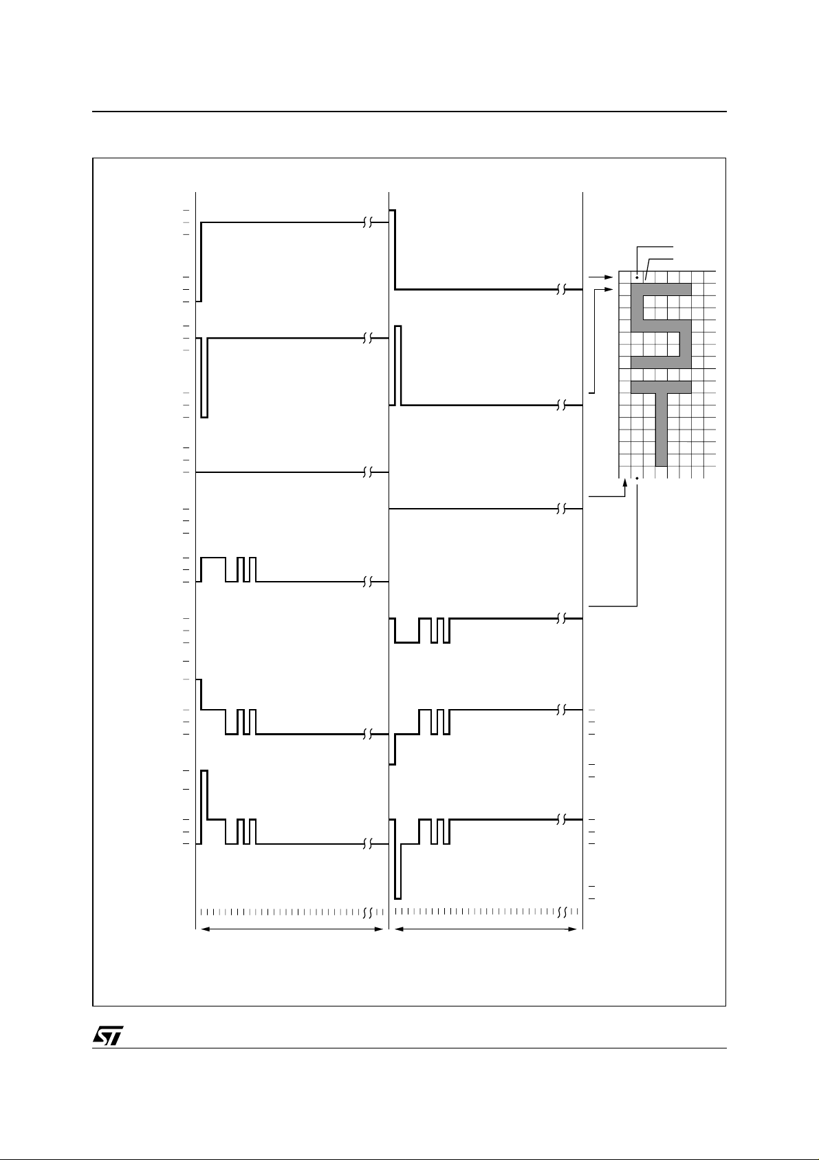
Figure 3. Improved ALTH & PLESKO Driving Method
V
LCD
V
2
V
3
ROW 0
R0 (t)
V
4
V
5
V
SS
V
LCD
V
2
V
3
ROW 1
R1 (t)
V
4
V
5
V
SS
V
LCD
V
2
V
3
COL 0
C0 (t)
V
4
V
5
V
SS
V
LCD
V
2
V
3
COL 1
C1 (t)
V
4
V
5
V
SS
V
- V
LCD
SS
V3 - V
SS
STE2004
∆V1(t)
∆V
(t)
2
V
V
state1
state2
- V
V
LCD
(t)
V3 - V
V
- V
LCD
V3 - V
- V
V
LCD
(t)
V3 - V
(t) = C1(t) - R0(t)
∆V
1
∆V
(t) = C1(t) - R1(t)
2
2
0V
SS
SS
SS
2
0V
SS
0 1 2 3 4 5 6 7 8 9 64
.......
FRAME n FRAME n + 1
0 1 2 3 4 5 6 7 8 9 64
.....
.......
.....
V
4 - V5
0V
V
SS - V5
V4 - V
VSS - V
V
4 - V5
0V
V
SS - V5
V4 - V
VSS - V
D00IN1154
LCD
LCD
LCD
LCD
5/67
Page 6

STE2004
CIRCUIT DESCRIPTION
Supplies Voltages and Gro un ds
is supply voltages to the internal voltage generator (see below). If the internal voltage generator is
V
DD2
not used, this should be c onnected to V
could be different form V
DD2
.
Internal Supply Voltage Ge nerator
The IC has a fully integrated (no external capacitors required) charge pump for the Liquid Crystal Display
supply voltage generation. T he m ultiplyin g fac tor can be program m ed t o be : Aut o, X 5, X4, X3, X 2, us ing
the ’set CP Multiplication’ Command. If Auto is set, the multiplying factor is automatically selected to have
the lowest current consumption in every condition. This make possible to have an input voltage that changes over time and a constant V
CDSENSE
pad. For this voltage, eight different temperature coefficients (TC, rate of change with
voltage. The output voltage (V
LCD
temperature) can be programmed using TC1 & TC 0 or T2, T1 and T0 bits. This will ensure no contrast
degradation over the LCD operating range.
An external supply could be connected to V
such event the internal voltage generator must be programmed to zero (PRS = [0;0], Vop = 0 - Reset condition) and the Charge pump (CP[0;0]) set to 5x or Auto Mode.
Oscillator
A fully integrated oscillator (requires no externa l com ponen ts) is presen t to provi de t he clock f or t he Display System. When u sed the O SC pad must be connec ted to V
used and fed into the OSC pin.If an external oscillator is used, it must be alwa ys pres ent wh en STE2 004
is not in power down mode. An oscillator out is provided on the OSCOUT Pad to cascade two or more
drivers.
Master/Slave Mode
STE2004 support the Master Slave working Mode for Both Control Logic and Charge Pump. This function
allows to drive matrix such as 204x65 or 102x 130 using two synchronized STE2004 and the internal
Charge Pump of both device.
If M/S
is connected to VDD1, the driver is configured to work in Master Mode. When STE2004 is in Master
Mode the Vsense_Slave P in is disabled and is possib le to control the VLCD value using Vop Bits. The
Master Time Generator outputs on FR_OUT and on OSC_O UT the relevant timing referen ces.
If M/S
is connected to GND, the driver i s configured to wo rk in Slave Mode. When S TE2004 is i n Slave
Mode, the VLCD configuration set by Vop registers and the thermal compensation slope set by TC register
are neglected. The VLCD Value generated is equal to the Voltage value present on Vsense_Slave Pin so
the slave configuration can follow t he master c onfiguration. The onl y recognized configuration is Vop=0
that forces the Charge Pump to be in off state whatever is the value of Vsense_aux.
To Synchronize the Master & Slave timing circuits, the slave driver FR_IN pad must be connected to Master Driver FR_OUT pad and Slave Driver OSC_IN pad must be connected to the master driver OSC_OUT
Pad (Fig. 4). This conn ection ensu re a syn chronization at bot h Fram e level (R0 on the m aster is driven
together with the Slave R0 driver) and at Osc illator Level (sam e Frame freque ncy on the master and on
the slave). If the Synchronization at Frame level is not required, FR_IN pin must be connected toVDD1 or
to VDD1_aux (Fig. 5).
During Power Up Procesure, Master device must be forced to exit from power down before the slave device. To enter in PowerDown Mode, Slave Device must be forced in Power Down state before Master Device.
V
DD1
DD2
pad. V
2VLCD⋅
------------------------ - 200mV+≥
n4+()
to supply the LCD without using the internal generator. In
LCD
supplies the rest of the IC. V
DD1
) is tightly controlled through the V
LCD
pad. An external oscillator could be
DD1
supply voltage
DD1
L-
6/67
Page 7
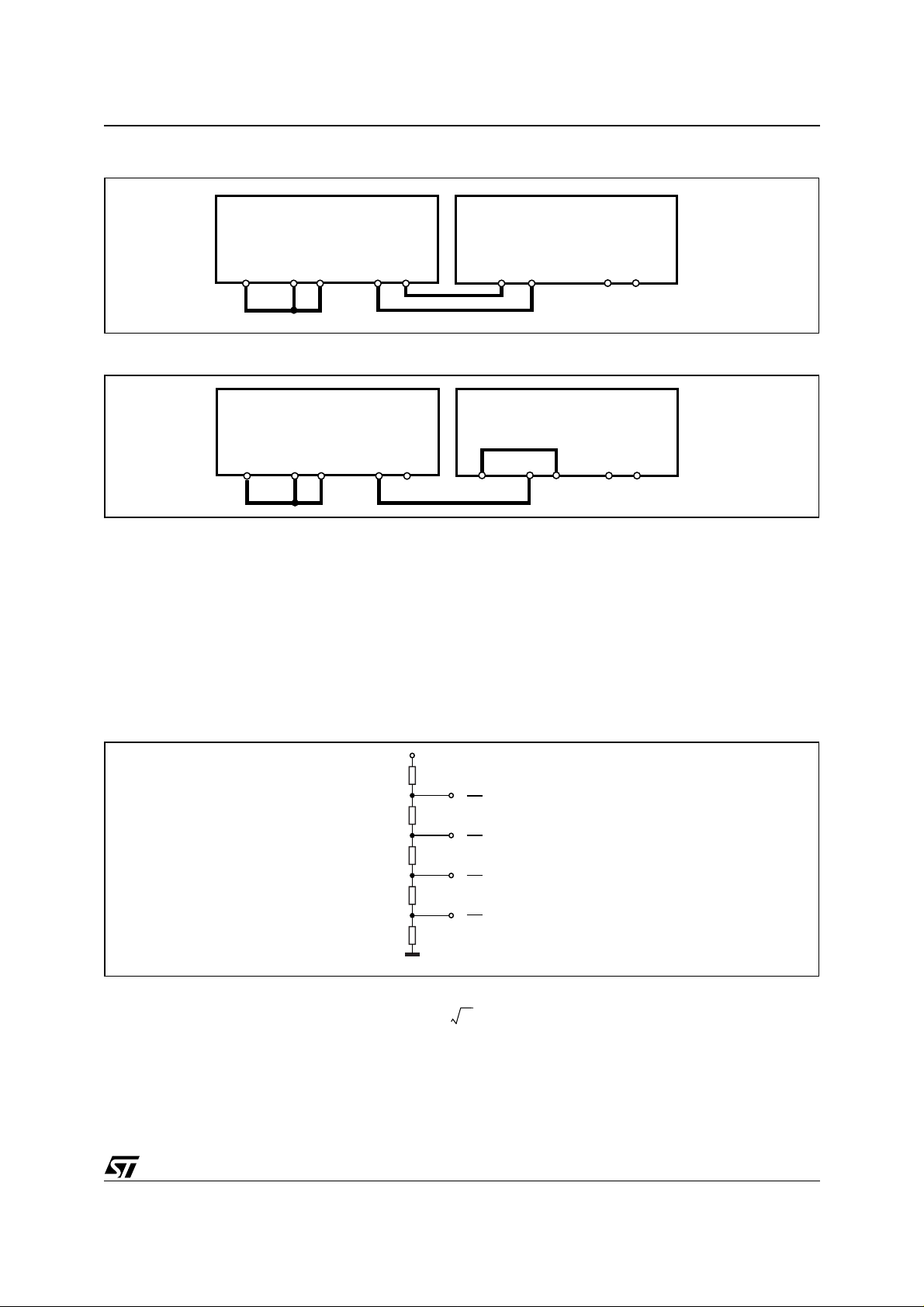
Figure 4. Master Slave Logic Connection with frame Synchronization
0
0
STE2004
STE2004
VDD1AUX
OSCOUT
FROUT OSCINFRINOSCIN FRIN
STE2004
OSCOUT FROUT
LR0219
Figure 5. Master Slave Logic Connection without frame Synchronization
STE2004
VDD1AUX
OSCOUT
FROUTOSCIN FRIN
VDD1AUX
STE2004
OSCIN
OSCOUT FROUT
FRIN
LR022
Bias Levels
To properly drive the LCD, six (Including VLCD and VSS) different voltage (Bias ) levels are generated.
The ratios among these levels and VLCD, s hould be selected acc ording to the MUX ratio (m). They are
established to be (Fig. 6):
V
LCD
n3+
------------ -
,
n4+
V
LCD
n2+
------------ -
,
n4+
V
LCD
2
------------ -
,
n4+
V
LCD
------------ -
,
n4+
1
V
LCD,VSS
Figure 6. Bias level Generator
V
R
R
nR
R
R
LCD
n + 3
n + 4
n + 2
n + 4
n + 4
n + 4
V
2
1
SS
·V
LCD
·V
LCD
·V
LCD
·V
LCD
D00IN115
thus providing an 1/(n+4) ratio, with n calculated from:
nm3–=
For m = 65, n = 5 and an 1/9 ratio is set.
For m = 49, n =4 and an 1/8 ratio is set.
The STE2004 provides three bits (BS0, BS1, BS2) for programming the desired Bias Ratio as shown below:
7/67
Page 8
STE2004
BS2 BS1 BS0 n
0007
0016
0105
0114
1003
1012
1101
1110
The following table Bias Level for m = 65 and m = 49 are provided:
Symbol m = 65 (1/9) m = 49 (1/8)
V1 V
V2 8/9*V
V3 7/9*V
V4 2/9*V V
V5 1/9 *V
V6 V
LCD
LCD
LCD
LCD
LCD
SS
V
7/8*V
6/8*V
2/8*V
1/8*V
V
LCD
LCD
LCD
LCD
LCD
SS
LCD Voltage Generation
The LCD Voltage at reference temperature (To = 27°C) can be set using the VOP register content according to
the following formula:
V
(T=To) = V
LCD
o = (Ai+VOP · B) (i=0,1,2)
LCD
with the following values:
Symbol Value Unit Note
Ao 2.95 V PRS = [0;0]
A1 6.83 V PRS = [0;1]
A2 10.71 V PRS = [1;0]
B 0.03 03 V
To 27 °C
Note that the three PRS values produce three adjacent ranges for VLCD. If the VOP register and PRS bits
are set to zero the internal voltage generator is switched off.
The proper value for the VLCD is a function of the Liquid Crystal Threshold Voltage (Vth) and of the Multiplexing Rate. A general expression for this is:
1m+
For MUX Rate m = 65 the ideal V
LCD
V
is:
LCD
----------------------------------- -
21
V
LCD(to)
⋅
= 6.85 · V
-------- -–
1
m
th
V
⋅=
th
than:
6.85 VthAi–⋅()
op
-----------------------------------------=
0.03
V
8/67
Page 9
STE2004
Temperature Coefficients
As the viscosity, and therefore the contrast, of the LCD are subject to change with temperature, there's
the need to vary the LCD Voltage with temperature. STE2004 provides the possibility to change the VLCD
in a linear fashion against temperature with eight different Temperature Coefficient selectable through T2,
T1 and T0 bits. Only four of them are available through basic instruction set.
NAME TC1 TC0 Value Unit
TC0 0 0
TC2 0 1
TC3 1 0
TC6 1 1
-0.7 · 10
-1.05· 10
-2.1 · 10
-0.0· 10
-3
-3
-3
-3
NAME T2 T1 T0 Value Unit
TC0 0 0 0
TC1 0 1 1
TC2 1 0 0
TC3 1 1 1
TC4 1 1 1
TC5 1 1 1
TC6 1 1 1
TC7 1 1 1
-0.35 · 10
-0.7 · 10
-1.05· 10
-1.4 · 10
-1.75· 10
-2.1 · 10
-0.0· 10
-2.3· 10
-3
-3
-3
-3
-3
-3
-3
-3
Figure 7.
1/ °C
1/°C
1/°C
1/°C
1/ °C
1/°C
1/°C
1/°C
1/°C
1/°C
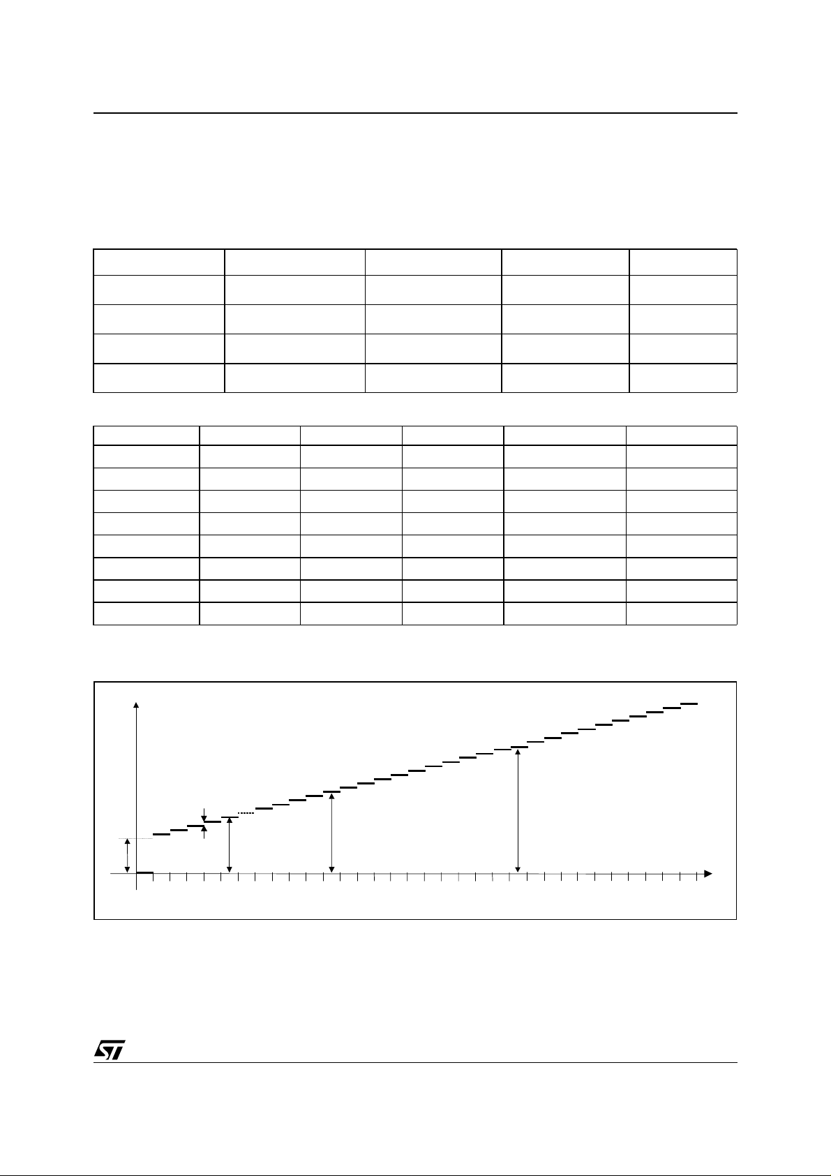
1/°C
1/°C
LCD
V
1
A
00h 01h 02h 03h 04h 05h ….
Finally, the V
B
1
0
A
+ B
7Ch 7Dh 7Eh
PRS = [0;0]
voltage at a given (T) temperature can be calculated as:
LCD
A
7Fh 00h 01h 02h
(T) = V
V
LCD
03h 04h
05h …. 7Ch
PRS = [0;1]
o · [1 + (T-To) · TC]
LCD
7Dh 7Eh 7Fh
2
A
00h 01h 02h 03h 04h
05h 7Ch
….
PRS = [1;0]
7Dh 7Eh 7Fh
O
V
9/67
Page 10

STE2004
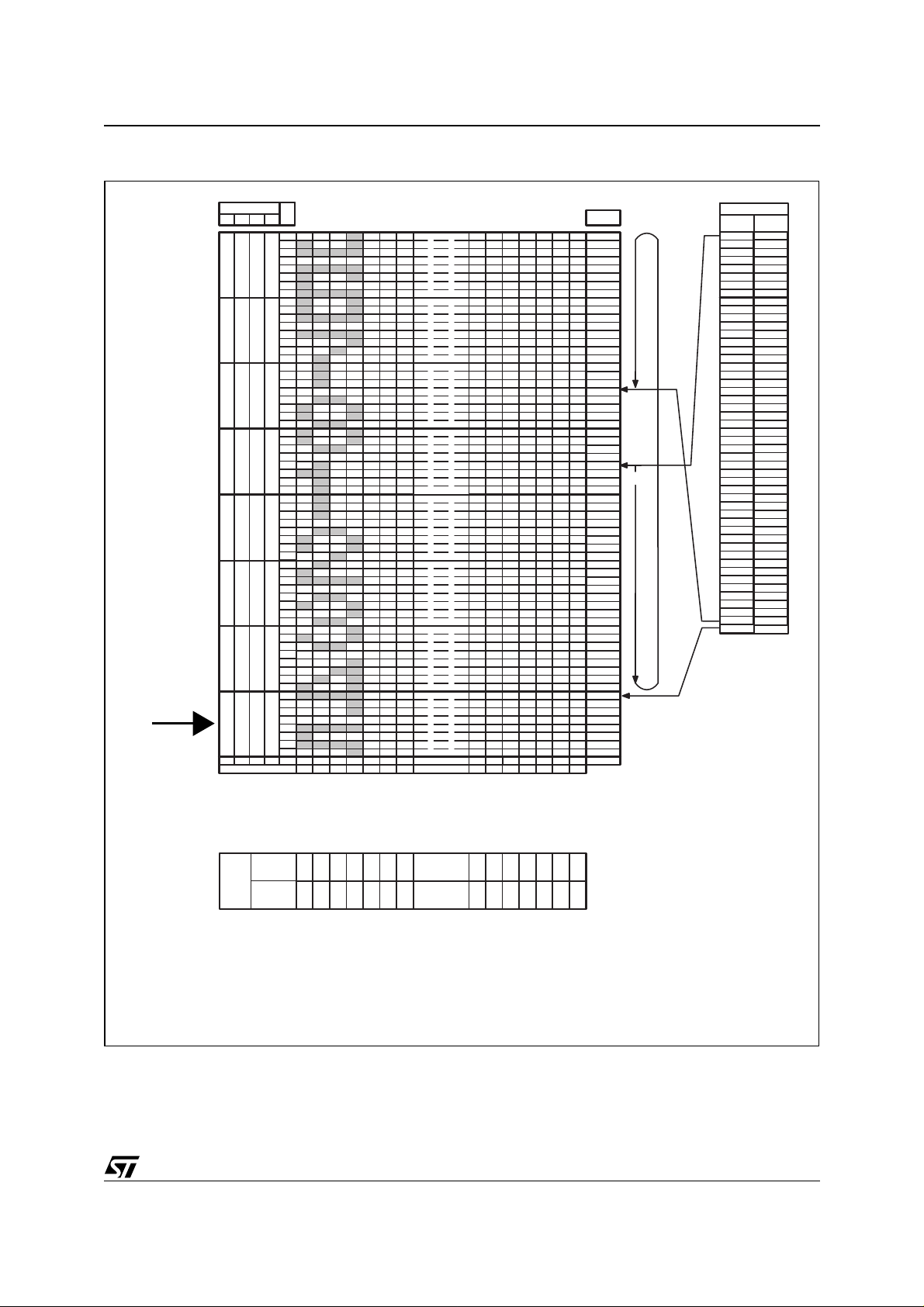
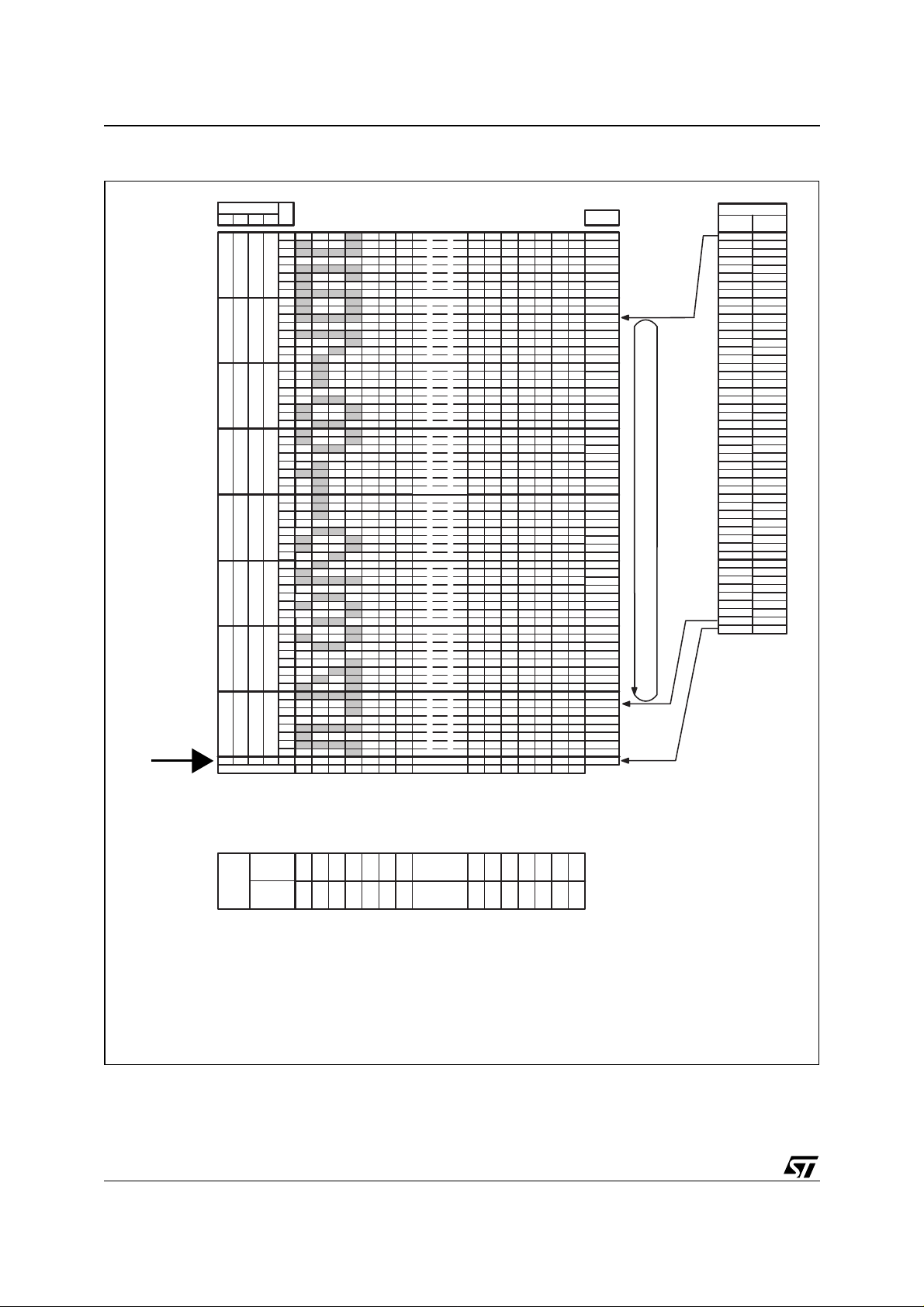
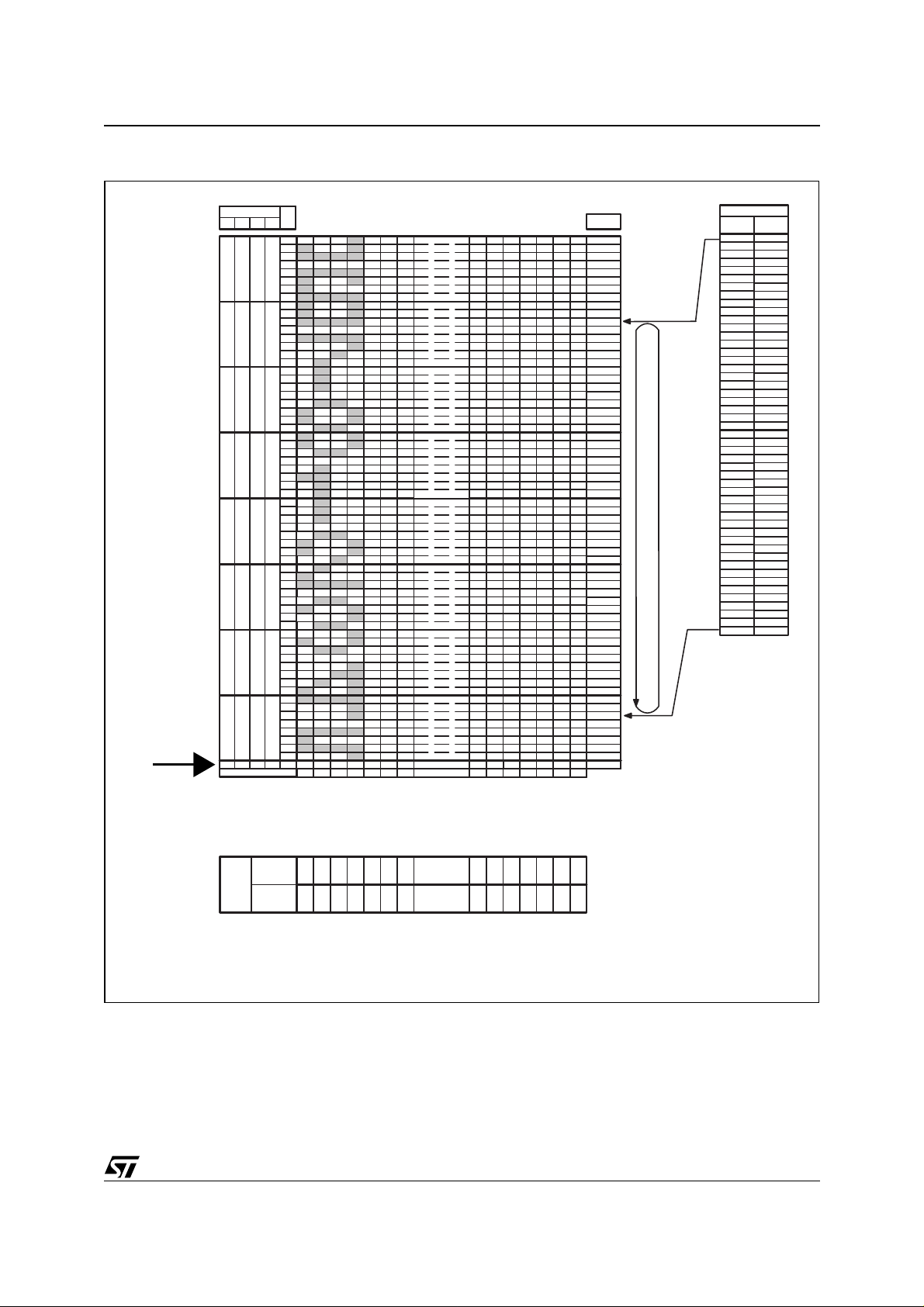
Display Data RAM
The STE2004, provides an 102X65 bits Static RAM to store Display data. This is organized into 9 (Bank0
to Bank8) banks with 102 Bytes. One of these Banks can be used for Icons. RAM access is accomplished
in either one of the Bus Interfaces provid ed (s ee be low). A llowed addres ses are X 0 to X101 (Horizontal)
and Y0 to Y8 (Vertical).
When writing to RAM, four addressing mode are provided:
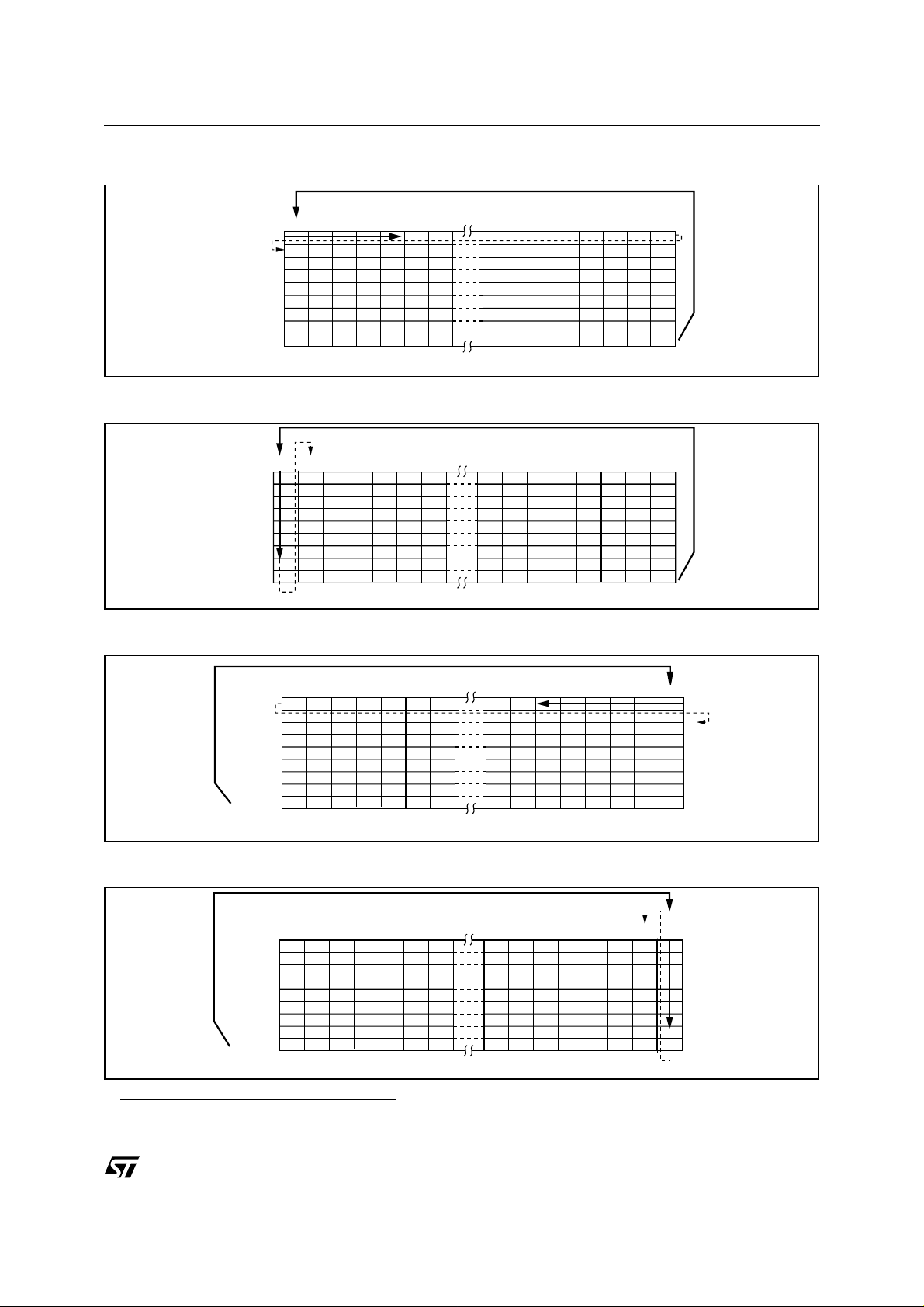
• Normal Horizontal (MX=0 and V=0), having the column with address X= 0 located on the left of the memory map. The X pointer is increased after each byte written. After the last column address (X=X-Carriage), Y address pointer is set to jump to the following bank and X restarts from X=0. (Fig. 8)
• Normal Vertical (MX=0 and V=1), having the column with address X= 0 located on the left of the memory
map. The Y pointer is increased after each byte written. After th e l ast Y b ank address (Y=Y-Carriage),
X address pointer is set to jump to next column and Y restarts from Y=0 (Fig. 9).
• Mirrored Horizontal (MX=1 and V=0), having the column with address X= 0 located on the right of the
memory map. The X pointer is increased af ter each byte written. After the last column address (X=XCarriage), Y address pointer is set to jump to the next bank and X restarts from X=0 (fig. 10).
• Mirrored Vertical (MX=1 and V=1), having the column with address X= 0 located on the right of the memory map. The Y pointer is increased after each byte written. After the last Y bank address (Y=Y-Carriage), the X pointer is set to jump to next column and Y restarts from Y=0 (fig. 11).
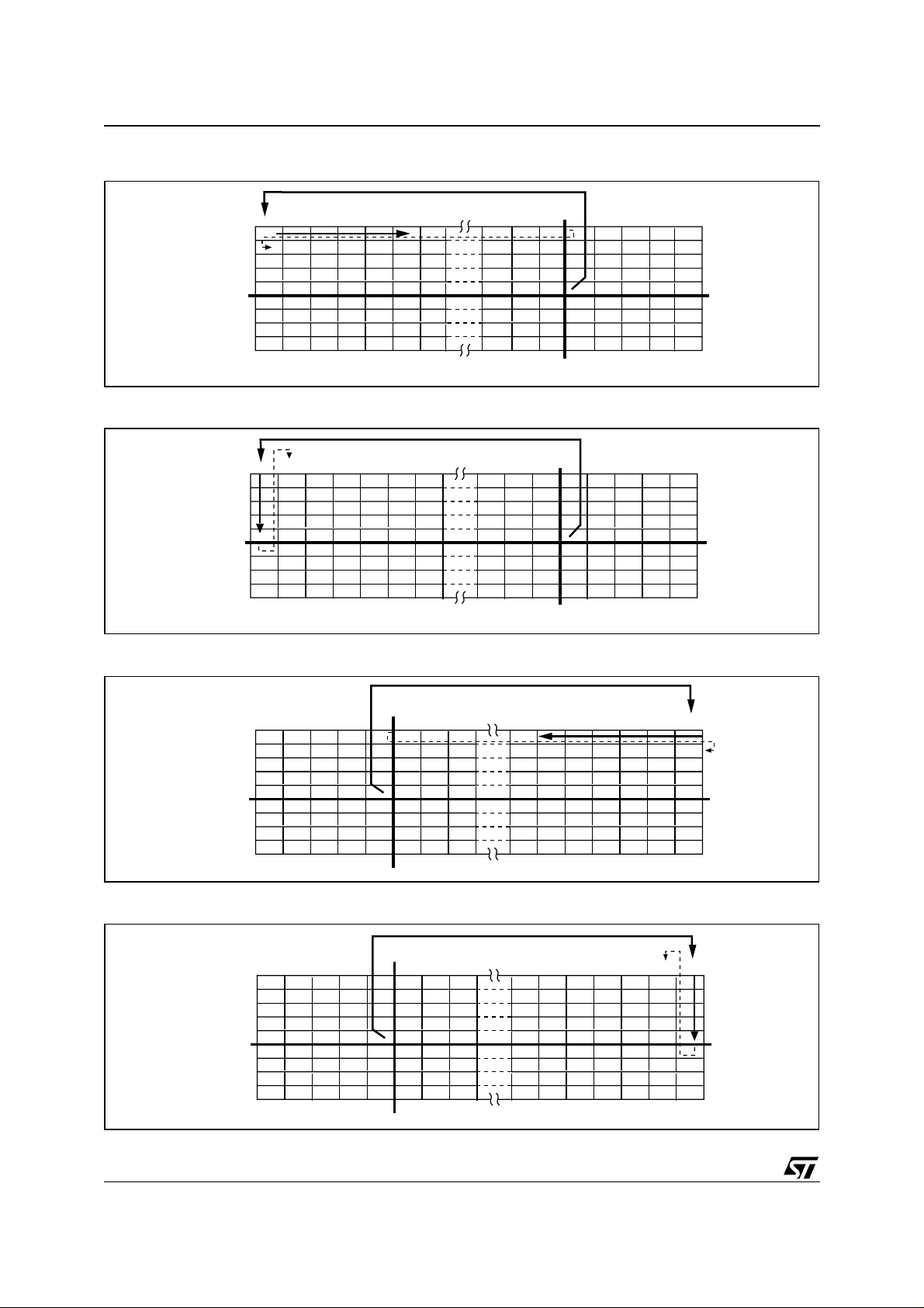
After the last allowed address (X;Y)=(X-Carriage; Y-Carriage), the address pointers always jump to the
cel l with addre ss (X;Y) = (0;0) (Fig. 12,13,14 & 15).
Data bytes in the memory could have the MSB either on top (D0 = 0, Fig.16) or on the bottom (D0=1, Fig.
17).
The STE2004 provides also means to alter the normal output addressing. A mirroring of the Display along
the X axis is enabled setting t o a l ogic one MY bit.This function does n't af fect t he cont ent of the me mory
map. It is only related to the memory read process.
When ICON MODE=1 the Icon Row is not mirrored with MY and is not scrolled.
When ICON MODE=0 the Icon Row is like an other graphic line and is mirrored and scrolled.
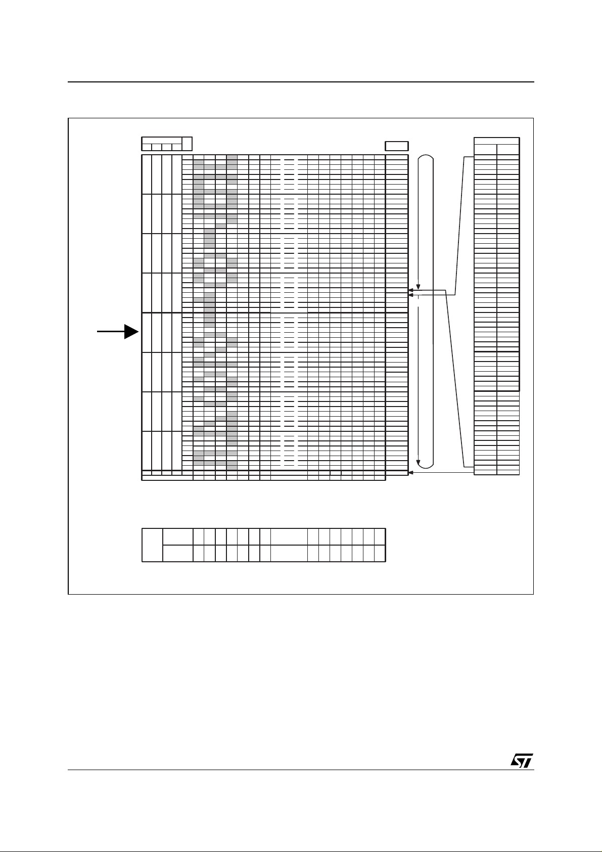
Three are the multiplex ratio available when the partial display mode i s disabled (MUX 33, MU X 49 and
MUX 65). Only a subset of writable rows are output on Row drivers in MUX 33,49 & 65 Mode.
When Y-Carriage<M U X/ 8, if Mux 49 is selected only the first 49 m emory rows are v isualized; if Mux 33 i s
selected only the first 33 memo ry rows are v isualized. Th e unused output row & colum n drivers m ust be
left floating.
When Y-Carri ag e<=MUX/8 the icon Bank is locat ed to BANK 8 i n MUX 65 Mode, to BANK6 in MUX 49
Mode and to BANK 4 in MUX 33 Mode.
In Mux 33 & 49 Mode, when Y-Carriage>MUX/8 lines only 33, 49 lines are visualized.
It is possible to select whic h l ines of DDRAM are c onnected on the output dri vers using the scrolling func-
tion (Range: 0-Y-Carriage*8). When Y-Carriage>MUX/8 lines, the icon row is moved in DDRAM to the
first row of the Bank correspondant to Y-CARRIAGE Return value, being always connected on the same
output Driver.
When MY=0, the icon Row is output on R64 in mux 65 mode, on R56 in MUX 49 and on R48 in MUX33.
When MY=1, and ICON MODE=0, the icon Row is output on R0 whatever is the MUX Rate.
10/67
Page 11
STE2004
2
Figure 8. Auto m at ic da ta RAM wri t in g sequence with V=0 and Data RAM N or m a l Form a t ( MX =0)1
BANK 0
BANK 1
BANK 2
BANK 3
BANK 4
BANK 5
BANK 6
BANK 7
BANK 8
0123 9899100101
LR0049
Figure 9. Auto m at ic da ta RAM wri t in g sequence with V=1 and Data RAM N or m a l Form a t ( MX =0)
BANK 0
BANK 1
BANK 2
BANK 3
BANK 4
BANK 5
BANK 6
BANK 7
BANK 8
010123 9899100101
LR0050
Figure 10. Automatic data RAM writing sequence with V=0 and Data RAM Mirrored Format (MX=1)
1
1
BANK 0
BANK 1
BANK 2
BANK 3
BANK 4
BANK 5
BANK 6
BANK 7
BANK 8
32109899100101
LR0051
Figure 11. Automatic data RAM writing sequence with V=1 and Data RAM Mirrored Format (MX=1)1
BANK 0
BANK 1
BANK 2
BANK 3
BANK 4
BANK 5
BANK 6
BANK 7
BANK 8
1. X Carriage=101; Y-Carriage = 8
10329899100101
LR005
11/67
Page 12
STE2004
3
4
6
Figure 12. Automatic data RAM writing sequence with X-Y Carriage Return (V=0; MX=0)
BANK 0
BANK 1
BANK 2
Y CARR
BANK 7
BANK 8
0123
X CARR
98 99 100 101
LR005
Figure 13. Automatic data RAM writing sequence with X-Y Carriage Return (V=1; MX=0)
0123
X CARR
BANK 0
BANK 1
BANK 2
Y CARR
BANK 7
BANK 8
98 99 100 101
LR005
Figure 14. Automatic data RAM writing sequence with X-Y Carriage Return (V=0; MX=1)
X CARR
BANK 0
BANK 1
BANK 2
Y CARR
BANK 7
BANK 8
1239899100101
0
LR0055
Figure 15. Automatic data RAM writing sequence with X-Y Carriage Return (V=1; MX=1)
X CARR
9899100101
BANK 0
BANK 1
BANK 2
Y CARR
BANK 7
BANK 8
0
123
LR005
12/67
Page 13
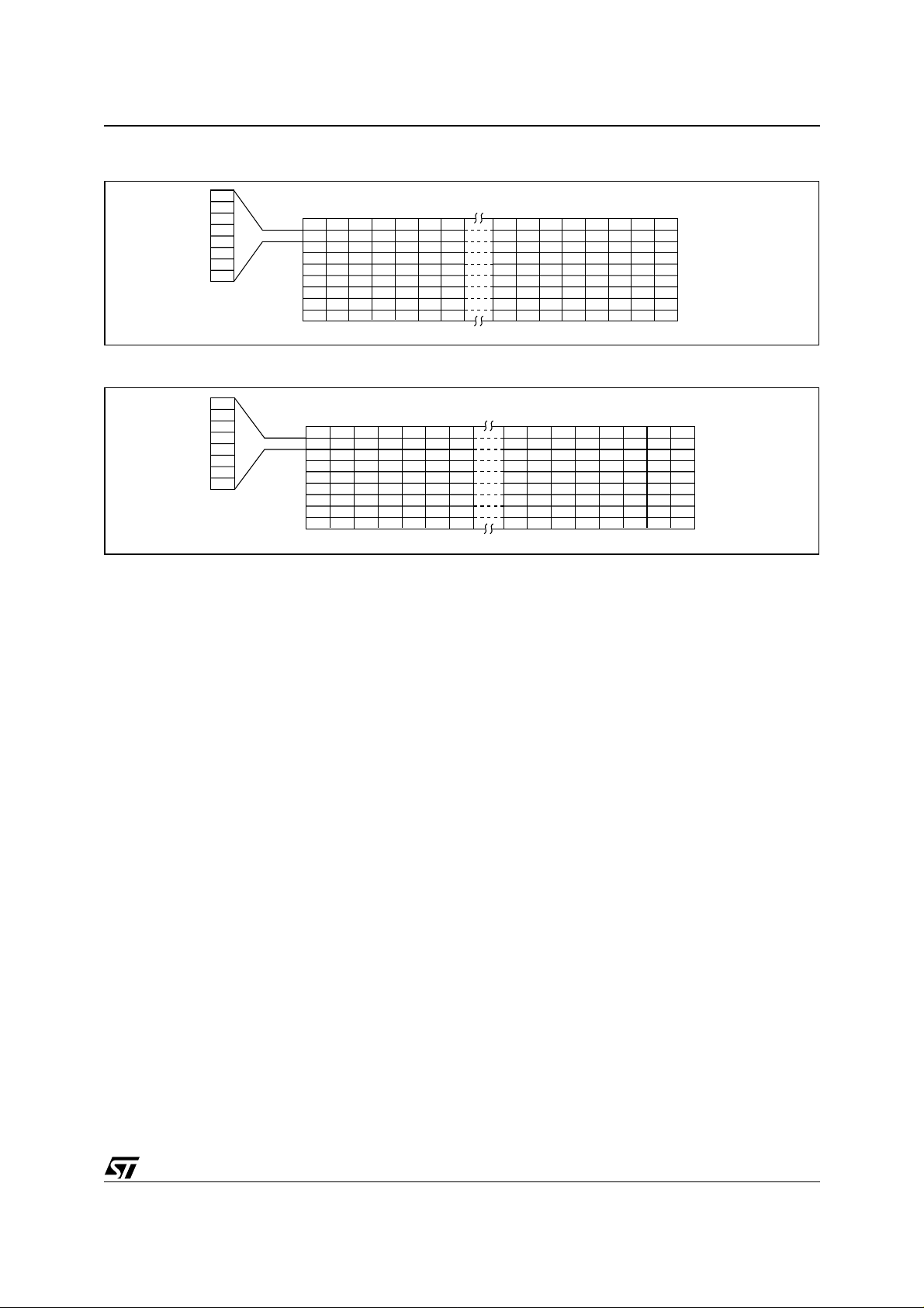
Figure 16. Data RA M Byte or ga n iza ti on with D0 = 0
8
MSB
0
1 2 3 98 99 100 101
LSB
BANK 0
BANK 1
BANK 2
BANK 3
BANK 4
BANK 5
BANK 6
BANK 7
BANK 8
Figure 17. Data RA M Byte or ga n iza ti on with D0 = 1
LSB
0123 9899100101
MSB
BANK 0
BANK 1
BANK 2
BANK 3
BANK 4
BANK 5
BANK 6
BANK 7
BANK 8
STE2004
LR0057
LR005
13/67
Page 14
STE2004
Figure 18. Memory Rows vs. Row Drivers Mapping ICON_MODE=1 and MUX 65
Y-CARRIAGE
Y Address
D3
D2 D1 D0
0
0
0
0
0
0
0
0
1
X address
D
a
t
a
D0
D1
D2
D3
0
0
0
D4
D5
D6
D7
D0
D1
D2
D3
0
1
0
D4
D5
D6
D7
D0
D1
D2
D3
1
0
0
D4
D5
D6
D7
D0
D1
D2
D3
1
1
0
D4
D5
D6
D7
D0
D1
D2
D3
0
0
1
D4
D5
D6
D7
D0
D1
D2
D3
0
1
1
D4
D5
D6
D7
D0
D1
D2
D3
1
0
1
D4
D5
D6
D7
D0
D1
D2
D3
1
1
1
D4
D5
D6
D7
0
0
0
D0
00H
02H 06H03H 04H 05H
01H
Page 0
Page 1
Page 2
Page 3
Page 4
Page 5
Page 6
Page 7
Page 8
5FH
61H 65H62H 63H 64H
60H
Line
Address
00H
01H
02H
03H
04H
05H
06H
07H
08H
09H
0AH
0BH
0CH
0DH
0EH
0FH
10H
11H
12H
13H
14H
15H
16H
17H
18H
19H
1AH
1BH
1CH
1DH
1EH
1FH
20H
21H
22H
23H
24H
25H
26H
27H
28H
29H
2AH
2BH
2CH
2DH
2EH
2FH
30H
31H
32H
33H
34H
35H
36H
37H
38H
39H
3AH
3BH
3CH
3DH
3EH
3FH
Scrolling Pointer
ROW Output
Normal
Reverse
direction
direction
R0
R1
R2
R3
R4
R5
R6
R7
R8
R9
R10
R11
R12
R13
R14
R15
R16
R17
R18
R19
R20
R21
R22
R23
R24
R25
R26
R27
R28
R29
R30
R31
R32
R33
R34
R35
R36
R37
R38
R39
R40
R41
R42
R43
R44
R45
R46
R47
R48
R49
R50
R51
R52
R53
R54
R55
R56
R57
R58
R59
R60
R61
R62
R63
R64 R64
R63
R62
R61
R60
R59
R58
R57
R56
R55
R54
R53
R52
R51
R50
R49
R48
R47
R46
R45
R44
R43
R42
R41
R40
R39
R38
R37
R36
R35
R34
R33
R32
R31
R30
R29
R28
R27
R26
R25
R24
R23
R22
R21
R20
R19
R18
R17
R16
R15
R14
R13
R12
R11
R10
R9
R8
R7
R6
R5
R4
R3
R2
R1
R0
lr0268
14/67
COL
Output
C
C
O
L
C
O
L
100 99
C
O
O
L
L
C
C
O
O
L
L
98 979695
C
O
L
C
O
L
C
Normal
O
L
Direction
0 1011 2 3 4 5 6 1009998979695
C
Reverse
O
L
Direction
101
C
C
C
C
O
O
L
L
C
C
O
O
L
L
C
C
C
O
L
C
O
L
6
C
O
O
O
L
L
L
C
C
C
O
O
O
L
L
L
4
5
C
O
O
O
L
L
L
C
C
C
O
O
O
L
L
L
0
123
Page 15
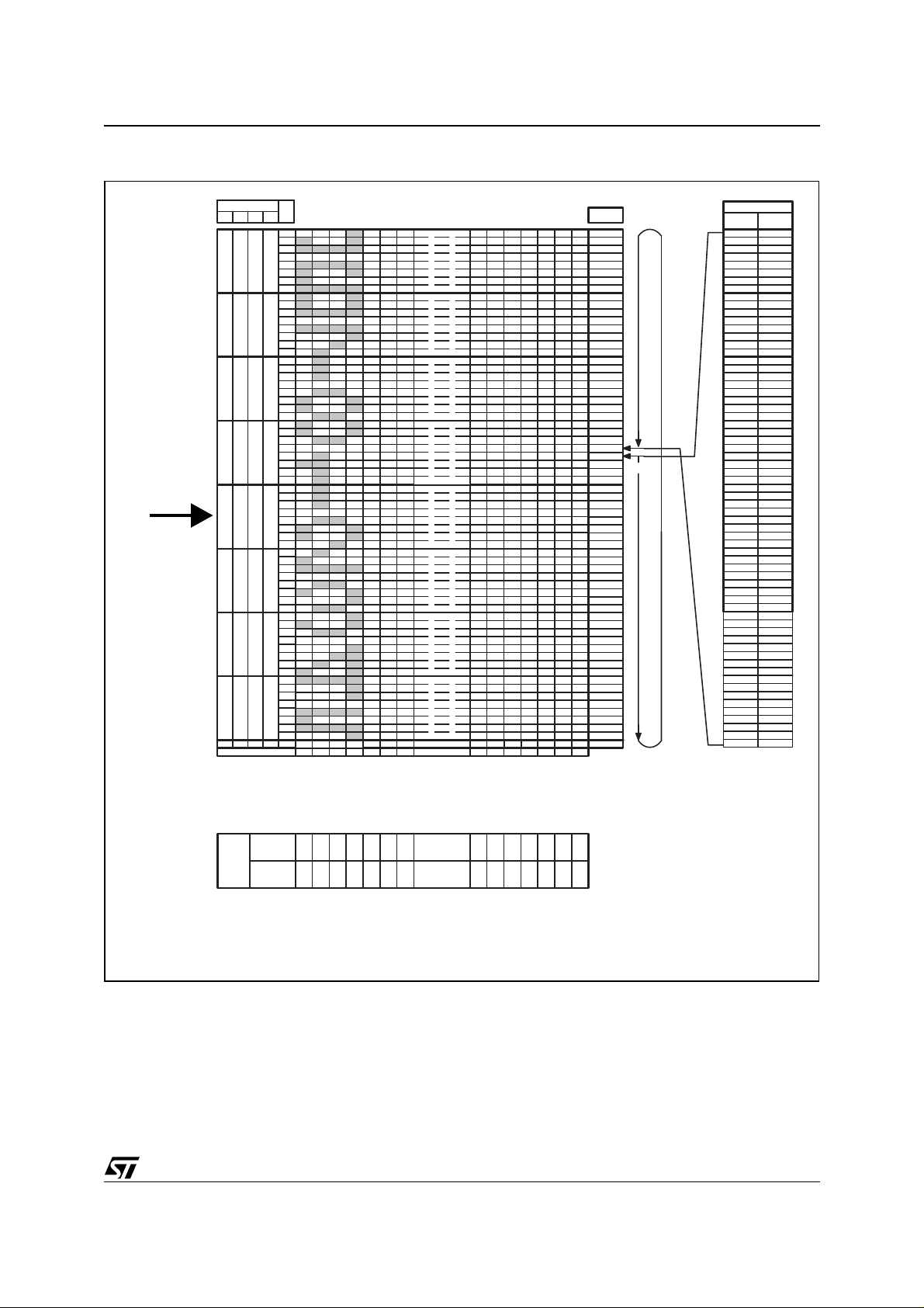
Figure 19. Memory Rows vs. Row Drivers Mapping ICON_MODE=0 and MUX 65
STE2004
Y-CARRIAGE
Y Address
D3
D2 D1 D0
0
0
0
0
0
0
0
0
0
1
0
1
0
1
0
1
0
1
X address
D
a
t
a
D0
D1
D2
D3
0
0
D4
D5
D6
D7
D0
D1
D2
D3
0
1
D4
D5
D6
D7
D0
D1
D2
D3
1
0
D4
D5
D6
D7
D0
D1
D2
D3
1
1
D4
D5
D6
D7
D0
D1
D2
D3
0
0
D4
D5
D6
D7
D0
D1
D2
D3
0
1
D4
D5
D6
D7
D0
D1
D2
D3
1
0
D4
D5
D6
D7
D0
D1
D2
D3
1
1
D4
D5
D6
D7
0
0
D0
00H
02H 06H03H 04H 05H
01H
Page 0
Page 1
Page 2
Page 3
Page 4
Page 5
Page 6
Page 7
Page 8
5FH
61H 65H62H 63H 64H
60H
Line
Address
00H
01H
02H
03H
04H
05H
06H
07H
08H
09H
0AH
0BH
0CH
0DH
0EH
0FH
10H
11H
12H
13H
14H
15H
16H
17H
18H
19H
1AH
1BH
1CH
1DH
1EH
1FH
20H
21H
22H
23H
24H
25H
26H
27H
28H
29H
2AH
2BH
2CH
2DH
2EH
2FH
30H
31H
32H
33H
34H
35H
36H
37H
38H
39H
3AH
3BH
3CH
3DH
3EH
3FH
40H
Scrolling Pointer
ROW Output
Normal
direction
R0
R1
R2
R3
R4
R5
R6
R7
R8
R9
R10
R11
R12
R13
R14
R15
R16
R17
R18
R19
R20
R21
R22
R23
R24
R25
R26
R27
R28
R29
R30
R31
R32
R33
R34
R35
R36
R37
R38
R39
R40
R41
R42
R43
R44
R45
R46
R47
R48
R49
R50
R51
R52
R53
R54
R55
R56
R57
R58
R59
R60
R61
R62
R63
R64
Reverse
direction
R64
R63
R62
R61
R60
R59
R58
R57
R56
R55
R54
R53
R52
R51
R50
R49
R48
R47
R46
R45
R44
R43
R42
R41
R40
R39
R38
R37
R36
R35
R34
R33
R32
R31
R30
R29
R28
R27
R26
R25
R24
R23
R22
R21
R20
R19
R18
R17
R16
R15
R14
R13
R12
R11
R10
R9
R8
R7
R6
R5
R4
R3
R2
R1
R0
COL
Output
Normal
Direction
Reverse
Direction
C
C
C
C
O
L
C
O
L
100 99
C
O
O
L
L
C
C
O
O
L
L
98 979695
C
O
L
0
C
O
L
101
C
C
C
O
O
O
L
L
L
C
C
C
O
O
O
L
L
L
C
C
C
O
L
C
O
L
6
C
O
O
O
L
L
L
C
C
C
O
O
O
L
L
L
4
5
C
O
O
O
L
L
L
1011 2 3 4 5 6 1009998979695
C
C
C
O
O
O
L
L
L
0
123
lr0269
15/67
Page 16
STE2004
Figure 20. Memory Rows vs. Row Drivers Mapping ICON_MODE=1,
D
a
t
a
D0
D1
D2
D3
0
0
0
D4
D5
D6
D7
D0
D1
D2
D3
0
1
0
D4
D5
D6
D7
D0
D1
D2
D3
1
0
0
D4
D5
D6
D7
D0
D1
D2
D3
1
1
0
D4
D5
D6
D7
D0
D1
D2
D3
0
0
1
D4
D5
D6
D7
D0
D1
D2
D3
0
1
1
D4
D5
D6
D7
D0
D1
D2
D3
1
0
1
D4
D5
D6
D7
D0
D1
D2
D3
1
1
1
D4
D5
D6
D7
0
0
0
D0
00H
02H 06H03H 04H 05H
01H
Page 0
Page 1
Page 2
Page 3
Page 4
Page 5
Page 6
Page 7
Page 8
5FH
60H
61H 65H62H 63H 64H
Y-CARRIAGE
Y Address
D3
D2 D1 D0
0
0
0
0
0
0
0
0
1
X address
Y-Carriage<=6
Line
Address
00H
01H
02H
03H
04H
05H
06H
07H
08H
09H
0AH
0BH
0CH
0DH
0EH
0FH
10H
11H
12H
13H
14H
15H
16H
17H
18H
19H
1AH
1BH
1CH
1DH
1EH
1FH
20H
21H
22H
23H
24H
25H
26H
27H
28H
29H
2AH
2BH
2CH
2DH
2EH
2FH
30H
31H
32H
33H
34H
35H
36H
37H
38H
39H
3AH
3BH
3CH
3DH
3EH
3FH
and MUX 49
Scrolling Pointer
ROW Output
Normal
direction
R0
R1
R2
R3
R4
R5
R6
R7
R8
R9
R10
R11
R12
R13
R14
R15
R16
R17
R18
R19
R20
R21
R22
R23
R32
R33
R34
R35
R36
R37
R38
R39
R40
R41
R42
R43
R44
R45
R46
R47
R48
R49
R50
R51
R52
R53
R54
R55
R56
Reverse
direction
R55
R54
R53
R52
R51
R50
R49
R48
R47
R46
R45
R44
R43
R42
R41
R40
R39
R38
R37
R36
R35
R34
R33
R32
R23
R22
R21
R20
R19
R18
R17
R16
R15
R14
R13
R12
R11
R10
R9
R8
R7
R6
R5
R4
R3
R2
R1
R0
R56
16/67
COL
Output
Normal
Direction
Reverse
Direction
C
C
C
C
O
L
C
O
L
100 99
C
O
O
L
L
C
C
O
O
L
L
98 979695
C
O
L
0
C
O
L
101
C
C
C
O
O
O
L
L
L
C
C
C
O
O
O
L
L
L
C
C
C
O
L
C
O
L
6
C
O
O
O
L
L
L
C
C
C
O
O
O
L
L
L
4
5
C
O
O
O
L
L
L
1011 2 3 4 5 6 1009998979695
C
C
C
O
O
O
L
L
L
0
123
lr0270
Page 17
STE2004
Figure 21. Memory Rows vs. Row Drivers Mapping ICON_MODE=0,
D2 D1 D0
0
0
0
0
1
0
1
0
0
1
0
1
1
1
1
1
0
0
D
a
t
a
D0
D1
D2
D3
0
D4
D5
D6
D7
D0
D1
D2
D3
1
D4
D5
D6
D7
D0
D1
D2
D3
0
D4
D5
D6
D7
D0
D1
D2
D3
1
D4
D5
D6
D7
D0
D1
D2
D3
0
D4
D5
D6
D7
D0
D1
D2
D3
1
D4
D5
D6
D7
D0
D1
D2
D3
0
D4
D5
D6
D7
D0
D1
D2
D3
1
D4
D5
D6
D7
0
D0
00H
02H 06H03H 04H 05H
01H
Page 0
Page 1
Page 2
Page 3
Page 4
Page 5
Page 6
Page 7
Page 8
5FH
60H
Y-CARRIAGE
Y Address
D3
0
0
0
0
0
0
0
0
1
X address
Y-Carriage<=6
61H 65H62H 63H 64H
and MUX 49
Line
Address
00H
01H
02H
03H
04H
05H
06H
07H
08H
09H
0AH
0BH
0CH
0DH
0EH
0FH
10H
11H
12H
13H
14H
15H
16H
17H
18H
19H
1AH
1BH
1CH
1DH
Scrolling Pointer
1EH
1FH
20H
21H
22H
23H
24H
25H
26H
27H
28H
29H
2AH
2BH
2CH
2DH
2EH
2FH
30H
31H
32H
33H
34H
35H
36H
37H
38H
39H
3AH
3BH
3CH
3DH
3EH
3FH
ROW Output
Normal
direction
R0
R1
R2
R3
R4
R5
R6
R7
R8
R9
R10
R11
R12
R13
R14
R15
R16
R17
R18
R19
R20
R21
R22
R23
R32
R33
R34
R35
R36
R37
R38
R39
R40
R41
R42
R43
R44
R45
R46
R47
R48
R49
R50
R51
R52
R53
R54
R55
R56
Reverse
direction
R56
R55
R54
R53
R52
R51
R50
R49
R48
R47
R46
R45
R44
R43
R42
R41
R40
R39
R38
R37
R36
R35
R34
R33
R32
R23
R22
R21
R20
R19
R18
R17
R16
R15
R14
R13
R12
R11
R10
R9
R8
R7
R6
R5
R4
R3
R2
R1
R0
COL
Output
Normal
Direction
Reverse
Direction
C
C
C
C
O
L
C
O
L
100 99
C
O
O
L
L
C
C
O
O
L
L
98 979695
C
O
L
0
C
O
L
101
C
C
C
O
O
O
L
L
L
C
C
C
O
O
O
L
L
L
C
C
C
O
L
C
O
L
6
C
O
O
O
L
L
L
C
C
C
O
O
O
L
L
L
4
5
C
O
O
O
L
L
L
1011 2 3 4 5 6 1009998979695
C
C
C
O
O
O
L
L
L
0
123
lr0271
17/67
Page 18
STE2004
Figure 22.
Y-CARRIAGE
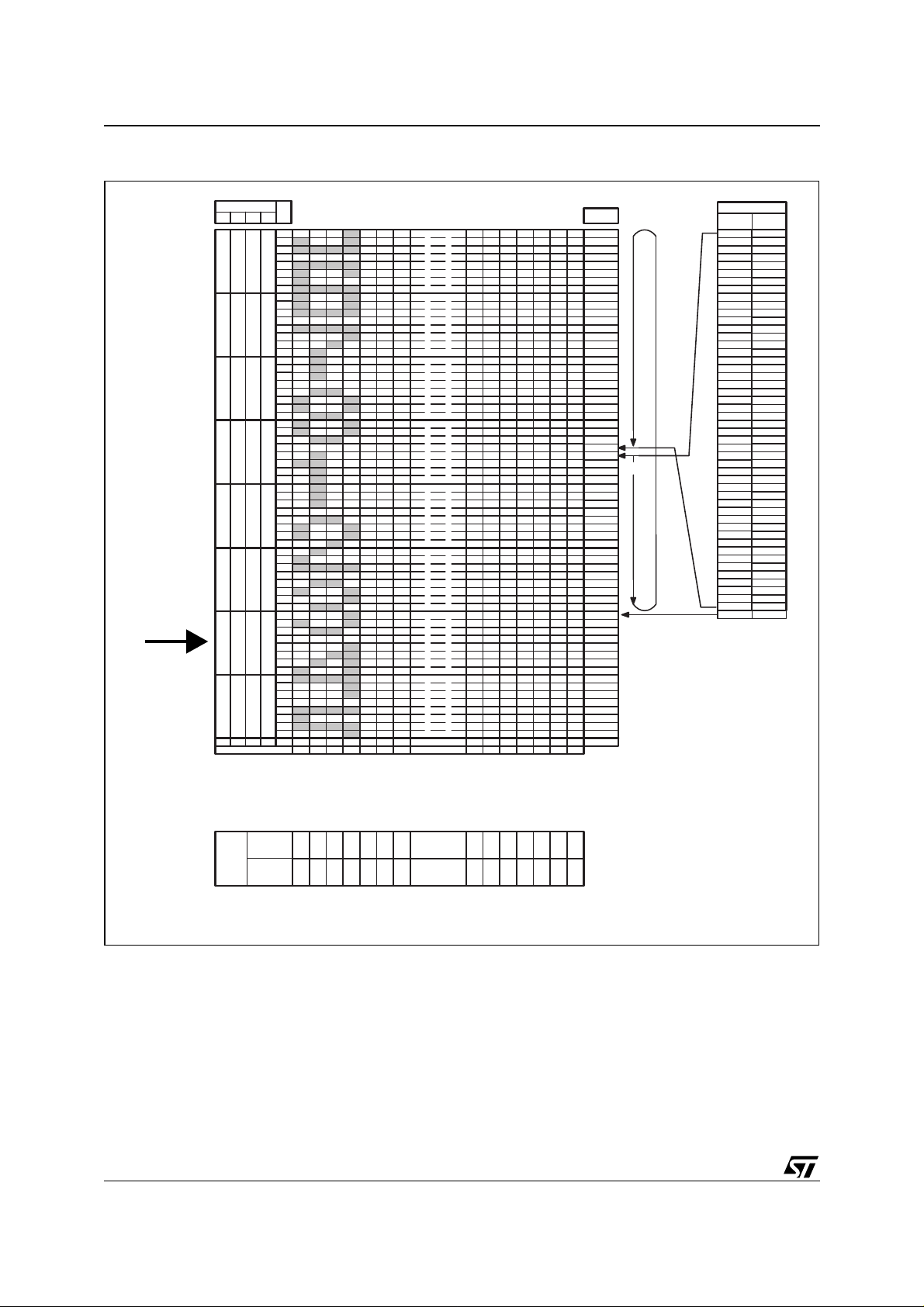
Memory Rows vs. Row Drivers Mapping ICON_MODE=0, Y-Carriage=7, Scrolling Pointer>07h and MUX 49
Y Address
D3
D2 D1 D0
0
0
0
0
0
0
0
0
1
X address
D
a
t
a
D0
D1
D2
D3
0
0
0
D4
D5
D6
D7
D0
D1
D2
D3
0
1
0
D4
D5
D6
D7
D0
D1
D2
D3
1
0
0
D4
D5
D6
D7
D0
D1
D2
D3
1
1
0
D4
D5
D6
D7
D0
D1
D2
D3
0
0
1
D4
D5
D6
D7
D0
D1
D2
D3
0
1
1
D4
D5
D6
D7
D0
D1
D2
D3
1
0
1
D4
D5
D6
D7
D0
D1
D2
D3
1
1
1
D4
D5
D6
D7
0
0
0
D0
00H
02H 06H03H 04H 05H
01H
Page 0
Page 1
Page 2
Page 3
Page 4
Page 5
Page 6
Page 7
Page 8
5FH
60H
61H 65H62H 63H 64H
Line
Address
00H
01H
02H
03H
04H
05H
06H
07H
08H
09H
0AH
0BH
0CH
0DH
0EH
0FH
10H
11H
12H
13H
14H
15H
16H
17H
18H
19H
1AH
1BH
1CH
1DH
1EH
1FH
20H
21H
22H
23H
24H
25H
26H
27H
28H
29H
2AH
2BH
2CH
2DH
2EH
2FH
30H
31H
32H
33H
34H
35H
36H
37H
38H
39H
3AH
3BH
3CH
3DH
3EH
3FH
Scrolling Pointer
ROW Output
Normal
direction
R0
R1
R2
R3
R4
R5
R6
R7
R8
R9
R10
R11
R12
R13
R14
R15
R16
R17
R18
R19
R20
R21
R22
R23
R32
R33
R34
R35
R36
R37
R38
R39
R40
R41
R42
R43
R44
R45
R46
R47
R48
R49
R50
R51
R52
R53
R54
R55
R56
Reverse
direction
R56
R55
R54
R53
R52
R51
R50
R49
R48
R47
R46
R45
R44
R43
R42
R41
R40
R39
R38
R37
R36
R35
R34
R33
R32
R23
R22
R21
R20
R19
R18
R17
R16
R15
R14
R13
R12
R11
R10
R9
R8
R7
R6
R5
R4
R3
R2
R1
R0
18/67
COL
Output
Normal
Direction
Reverse
Direction
101
C
C
C
C
O
L
C
O
L
100 99
C
O
O
L
L
C
C
O
O
L
L
98 979695
C
O
L
0
C
O
L
C
C
C
O
O
O
L
L
L
C
C
C
O
O
O
L
L
L
C
C
C
O
L
C
O
L
6
C
O
O
O
L
L
L
C
C
C
O
O
O
L
L
L
4
5
C
O
O
O
L
L
L
1011 2 3 4 5 6 1009998979695
C
C
C
O
O
O
L
L
L
0
123
lr0275
Page 19
STE2004
Figure 23.
Y-CARRIAGE
Memory Rows vs. Row Drivers Mapping ICON_MODE=1, Y-Carriage=7, Scrolling Pointer>07h and MUX 49
Y Address
D3
D2 D1 D0
0
0
0
0
0
0
0
0
1
X address
D
a
t
a
D0
D1
D2
D3
0
0
0
D4
D5
D6
D7
D0
D1
D2
D3
0
1
0
D4
D5
D6
D7
D0
D1
D2
D3
1
0
0
D4
D5
D6
D7
D0
D1
D2
D3
1
1
0
D4
D5
D6
D7
D0
D1
D2
D3
0
0
1
D4
D5
D6
D7
D0
D1
D2
D3
0
1
1
D4
D5
D6
D7
D0
D1
D2
D3
1
0
1
D4
D5
D6
D7
D0
D1
D2
D3
1
1
1
D4
D5
D6
D7
0
0
0
D0
00H
02H 06H03H 04H 05H
01H
Page 0
Page 1
Page 2
Page 3
Page 4
Page 5
Page 6
Page 7
Page 8
5FH
61H 65H62H 63H 64H
60H
Line
Address
00H
01H
02H
03H
04H
05H
06H
07H
08H
09H
0AH
0BH
0CH
0DH
0EH
0FH
10H
11H
12H
13H
14H
15H
16H
17H
18H
19H
1AH
1BH
1CH
1DH
1EH
1FH
20H
21H
22H
23H
24H
25H
26H
27H
28H
29H
2AH
2BH
2CH
2DH
2EH
2FH
30H
31H
32H
33H
34H
35H
36H
37H
38H
39H
3AH
3BH
3CH
3DH
3EH
3FH
Scrolling Pointer
ROW Output
Normal
direction
R0
R1
R2
R3
R4
R5
R6
R7
R8
R9
R10
R11
R12
R13
R14
R15
R16
R17
R18
R19
R20
R21
R22
R23
R32
R33
R34
R35
R36
R37
R38
R39
R40
R41
R42
R43
R44
R45
R46
R47
R48
R49
R50
R51
R52
R53
R54
R55
R56
Reverse
direction
R55
R54
R53
R52
R51
R50
R49
R48
R47
R46
R45
R44
R43
R42
R41
R40
R39
R38
R37
R36
R35
R34
R33
R32
R23
R22
R21
R20
R19
R18
R17
R16
R15
R14
R13
R12
R11
R10
R9
R8
R7
R6
R5
R4
R3
R2
R1
R0
R56
COL
Output
Normal
Direction
Reverse
Direction
101
C
C
C
C
O
L
C
O
L
100 99
C
O
O
L
L
C
C
O
O
L
L
98 979695
C
O
L
0
C
O
L
C
C
C
O
O
O
L
L
L
C
C
C
O
O
O
L
L
L
C
C
C
O
L
C
O
L
6
C
O
O
O
L
L
L
C
C
C
O
O
O
L
L
L
4
5
C
O
O
O
L
L
L
1011 2 3 4 5 6 1009998979695
C
C
C
O
O
O
L
L
L
0
123
lr0276
19/67
Page 20
STE2004
Figure 24.
Y-CARRIAGE
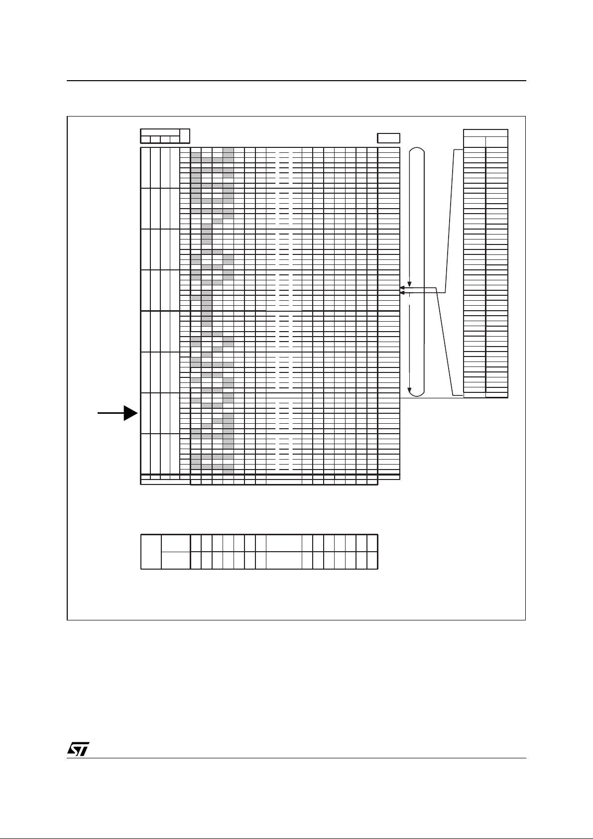
Memory Rows vs. Row Drivers Mapping ICON_MODE=1, Y-Carriage=8, Scrolling Pointer<10h and MUX 49
Y Address
D3
D2 D1 D0
0
0
0
0
0
0
0
0
1
X address
D
a
t
a
D0
D1
D2
D3
0
0
0
D4
D5
D6
D7
D0
D1
D2
D3
0
1
0
D4
D5
D6
D7
D0
D1
D2
D3
1
0
0
D4
D5
D6
D7
D0
D1
D2
D3
1
1
0
D4
D5
D6
D7
D0
D1
D2
D3
0
0
1
D4
D5
D6
D7
D0
D1
D2
D3
0
1
1
D4
D5
D6
D7
D0
D1
D2
D3
1
0
1
D4
D5
D6
D7
D0
D1
D2
D3
1
1
1
D4
D5
D6
D7
0
0
0
D0
00H
02H 06H03H 04H 05H
01H
Page 0
Page 1
Page 2
Page 3
Page 4
Page 5
Page 6
Page 7
Page 8
5FH
60H
61H 65H62H 63H 64H
Line
Address
00H
01H
02H
03H
04H
05H
06H
07H
08H
09H
0AH
0BH
0CH
0DH
0EH
0FH
10H
11H
12H
13H
14H
15H
16H
17H
18H
19H
1AH
1BH
1CH
1DH
1EH
1FH
20H
21H
22H
23H
24H
25H
26H
27H
28H
29H
2AH
2BH
2CH
2DH
2EH
2FH
30H
31H
32H
33H
34H
35H
36H
37H
38H
39H
3AH
3BH
3CH
3DH
3EH
3FH
Scrolling Pointer
ROW Output
Normal
direction
R0
R1
R2
R3
R4
R5
R6
R7
R8
R9
R10
R11
R12
R13
R14
R15
R16
R17
R18
R19
R20
R21
R22
R23
R32
R33
R34
R35
R36
R37
R38
R39
R40
R41
R42
R43
R44
R45
R46
R47
R48
R49
R50
R51
R52
R53
R54
R55
R56
Reverse
direction
R55
R54
R53
R52
R51
R50
R49
R48
R47
R46
R45
R44
R43
R42
R41
R40
R39
R38
R37
R36
R35
R34
R33
R32
R23
R22
R21
R20
R19
R18
R17
R16
R15
R14
R13
R12
R11
R10
R9
R8
R7
R6
R5
R4
R3
R2
R1
R0
R56
20/67
COL
Output
Normal
Direction
Reverse
Direction
101
C
C
C
C
O
L
C
O
L
100 99
C
O
O
L
L
C
C
O
O
L
L
98 979695
C
O
L
0
C
O
L
C
C
C
O
O
O
L
L
L
C
C
C
O
O
O
L
L
L
C
C
C
O
L
C
O
L
6
C
O
O
O
L
L
L
C
C
C
O
O
O
L
L
L
4
5
C
O
O
O
L
L
L
1011 2 3 4 5 6 1009998979695
C
C
C
O
O
O
L
L
L
0
123
LR0273
Page 21
STE2004
Figure 25.
Y-CARRIAGE
Memory Rows vs. Row Drivers Mapping ICON_MODE=0, Y-Carriage=8, Scrolling Pointer<10h and MUX 49
Y Address
D3
D2 D1 D0
0
0
0
0
0
0
0
0
0
1
0
1
0
1
0
1
0
1
X address
D
a
t
a
D0
D1
D2
D3
0
0
D4
D5
D6
D7
D0
D1
D2
D3
0
1
D4
D5
D6
D7
D0
D1
D2
D3
1
0
D4
D5
D6
D7
D0
D1
D2
D3
1
1
D4
D5
D6
D7
D0
D1
D2
D3
0
0
D4
D5
D6
D7
D0
D1
D2
D3
0
1
D4
D5
D6
D7
D0
D1
D2
D3
1
0
D4
D5
D6
D7
D0
D1
D2
D3
1
1
D4
D5
D6
D7
0
0
D0
00H
02H 06H03H 04H 05H
01H
Page 0
Page 1
Page 2
Page 3
Page 4
Page 5
Page 6
Page 7
Page 8
5FH
60H
61H 65H62H 63H 64H
Line
Address
00H
01H
02H
03H
04H
05H
06H
07H
08H
09H
0AH
0BH
0CH
0DH
0EH
0FH
10H
11H
12H
13H
14H
15H
16H
17H
18H
19H
1AH
1BH
1CH
1DH
1EH
1FH
20H
21H
22H
23H
24H
25H
26H
27H
28H
29H
2AH
2BH
2CH
2DH
2EH
2FH
30H
31H
32H
33H
34H
35H
36H
37H
38H
39H
3AH
3BH
3CH
3DH
3EH
3FH
Scrolling Pointer
ROW Output
Normal
direction
R0
R1
R2
R3
R4
R5
R6
R7
R8
R9
R10
R11
R12
R13
R14
R15
R16
R17
R18
R19
R20
R21
R22
R23
R32
R33
R34
R35
R36
R37
R38
R39
R40
R41
R42
R43
R44
R45
R46
R47
R48
R49
R50
R51
R52
R53
R54
R55
R56
Reverse
direction
R56
R55
R54
R53
R52
R51
R50
R49
R48
R47
R46
R45
R44
R43
R42
R41
R40
R39
R38
R37
R36
R35
R34
R33
R32
R23
R22
R21
R20
R19
R18
R17
R16
R15
R14
R13
R12
R11
R10
R9
R8
R7
R6
R5
R4
R3
R2
R1
R0
COL
Output
Normal
Direction
Reverse
Direction
101
C
C
C
C
O
L
C
O
L
100 99
C
O
O
L
L
C
C
O
O
L
L
98 979695
C
O
L
0
C
O
L
C
C
C
O
O
O
L
L
L
C
C
C
O
O
O
L
L
L
C
C
C
O
L
C
O
L
6
C
O
O
O
L
L
L
C
C
C
O
O
O
L
L
L
4
5
C
O
O
O
L
L
L
1011 2 3 4 5 6 1009998979695
C
C
C
O
O
O
L
L
L
0
123
LR0274
21/67
Page 22

STE2004
Figure 26.
Y-CARRIAGE
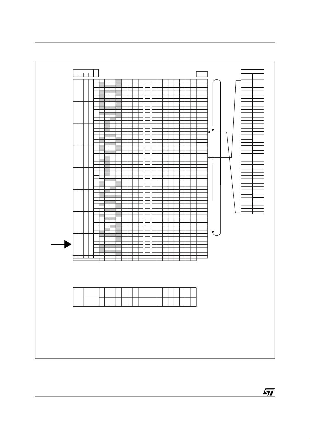
Memory Rows vs. Row Drivers Mapping ICON_MODE=1, Y-Carriage<=4 and MUX33
D2 D1 D0
0
0
0
0
1
0
1
0
0
1
0
1
1
1
1
1
0
0
D
a
t
a
D0
D1
D2
D3
0
D4
D5
D6
D7
D0
D1
D2
D3
1
D4
D5
D6
D7
D0
D1
D2
D3
0
D4
D5
D6
D7
D0
D1
D2
D3
1
D4
D5
D6
D7
D0
D1
D2
D3
0
D4
D5
D6
D7
D0
D1
D2
D3
1
D4
D5
D6
D7
D0
D1
D2
D3
0
D4
D5
D6
D7
D0
D1
D2
D3
1
D4
D5
D6
D7
0
D0
00H
02H 06H03H 04H 05H
01H
Page 0
Page 1
Page 2
Page 3
Page 4
Page 5
Page 6
Page 7
Page 8
5FH
61H 65H62H 63H 64H
60H
Line
Address
00H
01H
02H
03H
04H
05H
06H
07H
08H
09H
0AH
0BH
0CH
0DH
0EH
0FH
10H
11H
12H
13H
14H
15H
16H
17H
18H
19H
1AH
1BH
1CH
1DH
1EH
1FH
20H
21H
22H
23H
24H
25H
26H
27H
28H
29H
2AH
2BH
2CH
2DH
2EH
2FH
30H
31H
32H
33H
34H
35H
36H
37H
38H
39H
3AH
3BH
3CH
3DH
3EH
3FH
Scrolling Pointer
Y Address
D3
0
0
0
0
0
0
0
0
1
X address
ROW Output
Normal
direction
R0
R1
R2
R3
R4
R5
R6
R7
R8
R9
R10
R11
R12
R13
R14
R15
R32
R33
R34
R35
R36
R37
R38
R39
R40
R41
R42
R43
R44
R45
R46
R47
R48
Reverse
direction
R47
R46
R45
R44
R43
R42
R41
R40
R39
R38
R37
R36
R35
R34
R33
R32
R15
R14
R13
R12
R11
R10
R9
R8
R7
R6
R5
R4
R3
R2
R1
R0
R48
22/67
COL
Output
Normal
Direction
Reverse
Direction
101
C
C
C
C
O
L
C
O
L
100 99
C
O
O
L
L
C
C
O
O
L
L
98 979695
C
O
L
0
C
O
L
C
C
C
O
O
O
L
L
L
C
C
C
O
O
O
L
L
L
C
C
C
O
L
C
O
L
6
C
O
O
O
L
L
L
C
C
C
O
O
O
L
L
L
4
5
C
O
O
O
L
L
L
1011 2 3 4 5 6 1009998979695
C
C
C
O
O
O
L
L
L
0
123
LR0272
Page 23

STE2004
Figure 27.
Y-CARRIAGE
Memory Rows vs. Row Drivers Mapping ICON_MODE=0,
Y Address
D3
D2 D1 D0
0
0
0
0
0
0
0
0
1
X address
D
a
t
a
D0
D1
D2
D3
0
0
0
D4
D5
D6
D7
D0
D1
D2
D3
0
1
0
D4
D5
D6
D7
D0
D1
D2
D3
1
0
0
D4
D5
D6
D7
D0
D1
D2
D3
1
1
0
D4
D5
D6
D7
D0
D1
D2
D3
0
0
1
D4
D5
D6
D7
D0
D1
D2
D3
0
1
1
D4
D5
D6
D7
D0
D1
D2
D3
1
0
1
D4
D5
D6
D7
D0
D1
D2
D3
1
1
1
D4
D5
D6
D7
0
0
0
D0
00H
02H 06H03H 04H 05H
01H
Page 0
Page 1
Page 2
Page 3
Page 4
Page 5
Page 6
Page 7
Page 8
5FH
61H 65H62H 63H 64H
60H
Y-Carriage<=4
Line
Address
00H
01H
02H
03H
04H
05H
06H
07H
08H
09H
0AH
0BH
0CH
0DH
0EH
0FH
10H
11H
12H
13H
14H
15H
16H
17H
18H
19H
1AH
1BH
1CH
1DH
1EH
1FH
20H
21H
22H
23H
24H
25H
26H
27H
28H
29H
2AH
2BH
2CH
2DH
2EH
2FH
30H
31H
32H
33H
34H
35H
36H
37H
38H
39H
3AH
3BH
3CH
3DH
3EH
3FH
and MUX 33
Scrolling Pointer
ROW Output
Normal
direction
R0
R1
R2
R3
R4
R5
R6
R7
R8
R9
R10
R11
R12
R13
R14
R15
R32
R33
R34
R35
R36
R37
R38
R39
R40
R41
R42
R43
R44
R45
R46
R47
R48
Reverse
direction
R48
R47
R46
R45
R44
R43
R42
R41
R40
R39
R38
R37
R36
R35
R34
R33
R32
R15
R14
R13
R12
R11
R10
R9
R8
R7
R6
R5
R4
R3
R2
R1
R0
COL
Output
Normal
Direction
Reverse
Direction
101
C
C
C
C
O
L
C
O
L
100 99
C
O
O
L
L
C
C
O
O
L
L
98 979695
C
O
L
0
C
O
L
C
C
C
O
O
O
L
L
L
C
C
C
O
O
O
L
L
L
C
C
C
O
L
C
O
L
6
C
O
O
O
L
L
L
C
C
C
O
O
O
L
L
L
4
5
C
O
O
O
L
L
L
1011 2 3 4 5 6 1009998979695
C
C
C
O
O
O
L
L
L
0
123
LR0272
23/67
Page 24

STE2004
Figure 28. Row Drivers vs. LCD Panel Interconnection in MUX65 Mode
ICON
MUX 65
COLUMN DRIVERS
ROW DRIVERS
R32
R33
R34
R35
R36
R37
R38
R39
R40
R41
R42
R43
R44
R45
R46
R47
R48
R49
STE2004
R50
R51
R52
R53
R54
R55
R56
R57
R58
R59
R60
R61
R62
R63
R64
R 0
R 1
R 2
R 3
R 4
R 5
R 6
R 7
R 8
R 9
R10
R11
R12
R13
R14
R15
R16
ROW DRIVERS
R17
R18
R19
R20
R21
R22
R23
R24
R25
R26
R27
R28
R29
R30
R31
Figure 29. Row Drivers vs. LCD Panel Interconnection in MUX49 Mode
ICON
MUX 49
COLUMN DRIVERS
LR0109
24/67
ROW DRIVERS
R32
R33
R34
R35
R36
R37
R38
R39
R40
R41
R42
R43
R44
R45
R46
R47
R48
R49
STE2004
R50
R51
R52
R53
R54
R55
R56
R57
R58
R59
R60
R61
R62
R63
R64
R 0
R 1
R 2
R 3
R 4
R 5
R 6
R 7
R 8
R 9
R10
R11
R12
ROW DRIVERS
R13
R14
R15
R16
R17
R18
R19
R20
R21
R22
R23
R24
R25
R26
R27
R28
R29
R30
R31
LR0108
Page 25

Figure 30. Row Drivers vs. LCD Panel Interconnection in MUX33 Mode
ICON
MUX 33
COLUMN DRIVERS
STE2004
ROW DRIVERS
R32
R33
R34
R35
R36
R37
R38
R39
R40
R41
R42
R43
R44
R45
R46
R47
R48
R49
STE2004
R50
R51
R52
R53
R54
R55
R56
R57
R58
R59
R60
R61
R62
R63
R64
R 0
R 1
R 2
R 3
R 4
R 5
R 6
R 7
ROW DRIVERS
R 8
R 9
R10
R11
R12
R13
R14
R15
R16
R17
R18
R19
R20
R21
R22
R23
R24
R25
R26
R27
R28
R29
R30
R31
LR0107
25/67
Page 26

STE2004
BUS INTERFACES
To provide the widest flexibility and ease of use the STE2004 features Six different methods for interfacing
the host Controller. To select the desired interface the SEL1, SEL2 and SEL3 pads need to be connected
to a logic LOW (connect t o G ND) or a logic HIGH (connec t t o VDD). All the I/O pins o f the unu se d in terfaces must be connected to GND.
All interfaces are working while the STE2004 is in Power Down.
Table 1.
SEL3 SEL2 SEL1 Interface Note
000
0 0 1 SPI 4 lines 8 bit Read and Write
0 1 0 SPI 3 lines 8 bit Read and Write
0 1 1 Serial 3 lines 9 bit Read and Write
1 0 0 Parallel 8080-series Read and Write
1 0 1 Parallel 68000-series Read and Write
2
C Interface
I
2
C interface is a fully complying I2C bus specification, selectable to work in both Fast (400kHz Clock)
The I
and High Speed Mode (3.4MHz).
This bus is intended for communication between different Ics. It consists of two lines: one bi-directional for
data signals (SDA) and one for clock signals (SCL). Both the SDA and SCL lines must be connected to a
positive supply voltage via an active or passive pull-up.
The following protocol has been defined:
- Data transfer may be initiated only when the bus is not busy.
- During data transfer, the dat a line must remain stab le whenever the clock line is high. Ch anges in the
data line while the clock line is high will be interpreted as control signals.
Accordingly, the following bus conditions have been defined:
BUS not busy: Both data and clock lines remain High.
Start Data Transfer: A change in the state of the data line, from High to Low, while the clock is High, de-
fine the START condition.
Stop Data Transfer: A Change in the state of the data line, from low to High, while the clock signal is High,
defines the STOP condition.
Data Valid: The state of the data line repres ents vali d data when a fter a start condition, the data line is
stable for the duration of the High period of the clock signal. The data on the line may be changed during
the Low period of the clock signal. There is one clock pulse per bit of data.
Each data transfer is initiated with a start condition and terminated with a stop condition. The number of
data bytes transferred between the start and the stop conditions is not limited. The information is transmitted byte-wide and each receiver acknowledges with the ninth bit.
By definition, a device that gives out a m ess age is call ed "tran smitter", th e receiving dev ice that g ets the
signals is called "receiver". The device that controls the message is called "master". The devices that are
controlled by the master are called "slaves"
Acknowledge. Each byte of eight bits is followed by one acknowled ge bit. This acknow ledge bi t is a low
level put on the bus by the receiver, whereas t he mast er generates an extra acknow ledge related clock
pulse.
A slave receiver which is addressed must generate an acknowledge after the reception of each byte. Also,
a master receiver must generate an ackno wledge a fter the recep tion of ea ch byte that ha s been c locked
out of the slave transm itter. The device that acknowledges has to pull down the SD A_IN li ne during the
2
I
C
Read and Write; Fast and
High Speed Mode
26/67
Page 27

STE2004
9
acknowledge clock pulse. O f cou rse, set up and hold time must be taken int o account . A mast er receiver
must signal an end-of-data to the slave transmitter by not generating an acknowledge on the last byte that
has been clocked out of the slave. In this case, the transmitter must leave the data line High to enable the
master to generate the STOP condition.
Connecting SDA_IN and SDA_OUT together the SDA line become the standard data line. Having the acknowledge output (SDAOUT) separated from the serial data line is advantageous in Chip-On-Glass
(COG) applications. In COG applications where the track resistance from the SDAOUT pad to the system
SDA line can be significant, a potential divider is generated by the bus pull-up resistor and the Indium Tin
Oxide (ITO) track resistance. It is possible that during the acknowledge cycle the STE2004 will not be able
to create a valid logic 0 level. By splitting the SDA input from the output the device could be used in a mode
that ignores the acknowledge bit. In COG applications where the acknowledge cycle is required, it is necessary to minimize the track resistance from the SDACK pad to the system SDA line to guarantee a valid
LOW level.
To be compliant with the I
quence "S00001xxx". After this sequence no acknowledge pulse is generated.
Since no internal modification are applied to work in Hs-mode, the device is able to work in Hs-mode without detecting the master code.
Figure 31. Bit transfer and START,STOP conditions definition
2
C-bus Hs-mode specification the STE2004 is able to detect the special se-
DATA LINE
STABLE
DATA VALID
CLOCK
DATA
START
CONDITION
Figure 32. Acknowledgment on the
SCLK FROM
MASTER
DATA OUTPUT
BY TRANSMITTER
DATA OUTPUT
BY RECEIVER
START
I2C-bus
1
MSB LSB
CHANGE OF
DATA ALLOWED
289
STOP
CONDITION
CLOCK PULSE FOR
ACKNOWLEDGEMENT
LR006
LR0070
Communi c at io n P rot o c ol
The STE2004 is an I
2
C slave. The access to the dev ice is bi -directi onal sin ce dat a write and st at us read
are allowed.
Four are the device addresses available for the dev ice. All have in comm on the first 5 bits (01111). The
two least significant bit of the slave address are set by connecting the SA0 and SA1 inputs to a logic 0 or
to a logic 1.
To start the communication between the bus master and the slave LCD driver, the master must initiate a
START condition. Following this, the master sends an 8-bit byte, on the SDA bus line (Most significant bit
first). This consists of the 7-bit Device select Code, and the 1-bit Read/Write Designator (R/W
All slaves with the corresp onding add ress acknowledg e in parallel, a ll the others will ignore the I
).
2
C-bus
transfer.
27/67
Page 28

STE2004
Writing Mo de .
If the R/W bit is set to logic 0 the ST E2004 is set t o be a receiver. A fter the slaves acknowl edge one or
more command word follows to define the status of the device.
A command word is comp osed by t hree bytes. T he first is a control by te which de fines the Co an d D/C
values, the second and third are data bytes. The Co bit is the command MSB and defines if after this command will follow two data bytes and an other command word or if will follow a stream of data (Co = 1 Command word, Co = 0 Stream of data). The D/C
(D/C
= 1 RAM Data, D/C = 0 Command).
If Co =1 and D/C
= 0 the incoming data byte is decoded as a command, and if Co =1 and D/C =1, the
following data byte will be stored in the data RAM at the location specified by the data pointer.
Every byte of a command word must be acknowledged by all addressed units.
After the last control byte, if D/C
is set to a logic 1 the incoming data bytes are stored inside the STE2004
Display RAM starting at t he address specified by the data pointer. Th e data pointer is automaticall y updated after every byte written and in the end points to the last RAM location written.
Every byte must be acknowledged by all addressed units.
Reading Mode.
If the R/W bit is set to logic 1 the chip will output data immediately after the slave address. If the D/C bit
during the last write access, is set to a logic 0, the byte read is the status byte.
Figure 33. Communication Protocol
bit defines whether the data byte is a command or RAM data
WRITE MODE
DRIVER ACK
SS011110A0A
SLAVE ADDRESS
READ MODE
SS011110A1A
S
A
1
R/W
DRIVER ACK MASTER ACK
S
A
1
R/W
DRIVER ACK
A1 DC Control Byte DATA Byte ADC Control ByteA 0 DATA Byte A P
Co
COMMAND WORD CONTROL BYTE MSB........LSB
P
DRIVER ACK DRIVER ACK DRIVER ACK
Co LAST N> 0 BYTE
S
DRIVER
S
A
1
011110AR/
SLAVE ADDRESS
W
CoD
C
CONTROL BYTE
H
000 A
[1]H[0]HE
LR0008
28/67
Page 29

STE2004
SERIAL INTERFACES
STE2004 can fe ature three differ ent serial synchroniz ed interfaces with the host con troller. It is p ossible to select
a 3-lines SPI, a 4-lines SPI or 3-line 9 bits Serial Interface.
4-lines SPI interface
STE2004 4-lines serial inter face is a bi directional link betw een the display driv er and the application super visor.
It consists of four lines: one/two for data signals (SDIN, SOUT), one for clock signals (SCLK), one for the pe-
ripheral enable (CS
The serial interface is active only if the CS
consumption is zero. While CS
The STE2004 is always a slave on the bus and receive the com munication clock on the SCLK pin from the mas-
ter.
Information are exchanged by te-wide. During data transfer, the data l ine is sampl ed on the positi ve SCLK edge.
line status indicates whether the byte is a command (SD/C =0) or a data (SD/C =1); SD/C line is read on
SD/C
the eighth SCLK clock pulse during every byte transfer.
stays low after the last bit of a command/data byte, the serial interface expects the MSB of the next byte
If CS
at the next SCLK positive edge.
A reset pulse on RES
registers are cleared.
is low after the positive edge of RES, the serial interface is ready to receive data.
If CS
Throughout SDOUT can be read the driver I
allows to read I
steady state and during data write.
It is possible to short circuit SDOUT and SDIN and read I2 C addres s or status Byte without any additional li nes.
) and one for mode selection (SD/C).
line is set to a logic 0. When CS line is high the serial peripheral p ower
pin is high the serial interface is kept in reset.
pin interrupts the transmission. No data is written into the data RAM and all the internal
2
2
C slave address or Status byte is reported in Fig. 34 & 35. SDOUT is in High impedance in
C slave address or the status byte. The Command sequence that
Figure 34. 4-lines serial bus protocol - one byte transmission
CS
D/C
SCLK
SDIN
MSB LSB
Figure 35. 4-lines serial bus protocol - several byte transmission
CS
D/C
SCLK
SDIN
DB7 DB6 DB5 DB4 DB3 DB2 DB1 DB0 DB7 DB6 DB5 DB4 DB3 DB2 DB1 DB0 DB7 DB6 DB5
LR0071
LR0072
29/67
Page 30

STE2004
Figure 36. 4-lines serial bus protocol - I2C Address or Status Byte Read
CS
SCLK
Don't
Don't
Don't
Don't
Don't
SDIN
D/C
DB7 DB6 DB5 DB4 DB3 DB2 DB1 DB0
Care
Care
Care
Care
Care
Don't
Care
Don't
Care
Don't
Care
High-Z
SDOUT
High-Z
Command Write
Figure 37. 4-lines SPI Reading Sequence
READING SEQUENCE
Write a "00000000" Instruction
SDOUT Buffer becomes active (Low Impedence)
Source 8 pulses on SCLK and
Read the ID Number or the Status Byte On SDOUT
SDOUT Buffer Configured in High Impedence
DB7 DB6 DB5 DB4 DB3 DB2
ID Number
DB7 DB6 DB5 DB4 DB3 DB2
STATUS BYTE
DATA Read
1
DB1 DB0
DB1 DB0
High-Z
High-Z
LR00076
30/67
END OF READING SEQUENCE
note: 1) these data are not read by the display Diver
2) SDIN and SDOUT can be short circuited if the processor can configure
serial output buffers in high impedence during data read
.
LR0078
Page 31

STE2004
3-lines SPI Interface
The STE2004 3-lines serial Interface is a bidirectional link between the displa y driver and the application
supervisor.
It consists of three lines: o ne/ two for dat a si gnals (SDIN,SDOUT), one f or clock signals (SCLK) and one
for peripheral enable (CS
If the R/W bit is set to logic 0 the STE2004 is set to be a receiver. One or more command word follows to
define the status of the device.
A command word is composed by two bytes. The first is a control byte which defines Co, D/C
and HE values, the second is a data byte (fig 39). The Co bit is the command MSB and defines if after this
command will follow one data byte and an other command word or if will follow a stream of Commands or
a Steam of DDRAM Data (Co = 1 Command word, Co = 0 Stream of da ta). The D/C
the data byte is a command or DDRAM da ta (D/C
define the instruction Set Page if HE bit =1. If HE bit is set to 0 H[1;0] values are neglected and it is possible
to update the instruction set page number using only the related instruction in the instruction Set.
If Co =1 and D/C
= 0 the incoming data byte is decoded as a command, and if Co =1 and D/C =1, the
following data byte will be stored in the data RAM at the location specified by the data pointer.
After the last control byte, if D/C
Display Data RAM starting at the address specified by the data pointer. The data pointer is automatically
updated after every byte written and in the end points to the last RAM location written.
Throughout SDOUT can be read the driver I
that allows to read I
If the R bit is set to logic 0 and D/C=0, the I
C=0, the the I
2
C slave address is read
SDOUT is in High impedance in steady state and during data write.
It is possible to short circuit SDOUT and SDIN and read I
line.
).
= 1 RAM Data, D/C = 0 Com mand). The H[1;0] bits
is set to a logic 1 the incoming data bytes are stored inside the STE2004
2
2
C slave address or the Status byte is reported in Fig. 39 & 40.
C slave address or the status Byte. The Command sequence
2
C slave address is read; If the R bit is set to logic 1 and D/
2
C address or status byte without any additional
, R/W H[1;0]
bit defines whether
Figure 38. 3-lines serial interface protocol in Writing Mode
WRITE MODE
Control Byte
1
Co
COMMAND WORD CONTROL BYTE MSB........LSB
Control Byte
0 DATA Byte
0
LAST N> 0 BYTE
CONTROL BYTE MSB........LSB
Control Byte
1
0 DATA Byte
LAST N> 0 BYTE
CONTROL BYTE MSB........LSB
DATA Byte
DATA Byte
DATA Byte
Control Byte0 DATA Byte
Co LAST N> 0 BYTE
TRANSFERRED
ONLY COMMANDS
TRANSFERRED
ONLY DDRAM DATA
R
CoD
00
/
C
W
CONTROL BYTE
DATA Byte = Command if D/C=0
DATA Byte = DDRAM Data if D/C=1
LR0002
H
H
H
[0]
E
[1]
31/67
Page 32

STE2004
Figure 39. 3-lines SPI interface protocol in Reading Mode
CS
SCLK
Don't
SDIN
SDOUT
DB7 DB6 DB5 DB4 DB3 DB2 DB1 DB0
Co=1 D/C=0
"Command"
R/W=1
"Read"
High-Z
High-Z
Don't
Care
Care
DB7 DB6 DB5 DB4 DB3 DB2
DB7 DB6 DB5 DB4 DB3 DB2
Don't
Don't
Care
Care
ID-Number
STATUS BYTE
Don't
Care
Don't
Care
Don't
Don't
Care
Care
DB1 DB0
DB1 DB0
High-Z
High-Z
Command Write
Figure 40. 3-lines SPI Reading Sequence
READING SEQUENCE
Set Co bit =1, D/C Bit =0 R/W Bit =1
SDOUT Buffer become active (Low Impedence)
Source 8 pulses on SCLK and
ID-Number
Read the
SDOUT Buffer Configured in High Impedence
END OF READING SEQUENCE
note: 1) these data are not read by the display Diver
2) SDIN and SDOUT can be short circuited if the processor can configure
serial output buffers in high impedence during data read
DATA Read
or the Status Byte On SDOUT
1
.
LR0077
LR0079
3-lines 9 bits Serial Interface
The STE2004 3-lines serial Interface is a bidirectional link between the displa y driver and the application
supervisor.
It consists of three lines: one/two for data signals (SDIN, SDOUT), one for clock signals (SCLK) and one
for peripheral enable (CS
The serial interface is active only if the CS
power consumption is zero. While CS
).
line is set to a logic 0. When CS line is high the serial peripheral
pin is high the serial interface is kept in reset.
The STE2004 is always a s lave on the bus and receive t he comm unication cloc k on the SCLK pin from
the m aster.
Information are exchanged wo rd-wide. The word i s composed by 9 bit. The f irst bit is nam ed SD/C
indicates whether the following byte is a command (SD/C
=0) or Data Byte (SD/C =1). During data trans-
and
fer, the data line is sampled on the positive SCLK edge.
If CS
stays low after the last b it of a c om m and/data byte, the serial interface expects the SD/ C Bit of the
next word at the next SCLK positive edge.
A reset pulse on RES
32/67
pin interrupts the transmission. No data is written into the data RAM and all the in-
Page 33

ternal registers are cleared.
4
If CS
is low after the positive edge of RES, the serial interface is ready to receive data.
Throughout SDOUT can be rea d only the driver I
quence that allows to read I
2
C slave address or Status byte is reported in Fig. 43 & 44. SDOUT is in High
impedance in steady state and during data write.
It is possible to short circuit SDOUT and SDIN and read I
2
C slave address or the status byte. The Command se-
2
C address or status byte without any additional
line.
Figure 41. 3-lines serial bus protocol - one byte transmission
CS
SCLK
STE2004
SDIN
MSBSD/C
Figure 42. 3-lines serial bus protocol - several byte transmission
CS
SCLK
SDIN
DB7 DB6 DB5 DB4 DB3 DB2 DB1 DB0
DB7 DB6 DB5 DB4 DB3 DB2 DB1 DB0D/C
D/C DB7 DB6D/C
Figure 43. 3-lines serial interface protocol in Reading Mode
CS
SCLK
Don't
Don't
SDIN
SDOUT
DB7 DB6 DB5 DB4 DB3 DB2 DB1 DB0
SD/C
DB7SD/C
High-Z
High-Z
Don't
Care
Care
DB7 DB6 DB5 DB4 DB3 DB2
DB7 DB6 DB5 DB4 DB3 DB2
Don't
Care
Care
ID-Number
STATUS BYTE
Don't
Care
Don't
Care
LSB
Don't
Don't
Care
Care
DB1 DB0
DB1 DB0
LR0073
LR007
High-Z
High-Z
Command Write
DATA Read
LR0075
33/67
Page 34

STE2004
Figure 44. 3-lines Serial Reading Sequence
READING SEQUENCE
Write a "00000000" Instruction
SDOUT Buffer becomes active (Low Impedence)
Source 9 pulses on SCLK and
Read the ID Number or the Status Byte On SDOUT
SDOUT Buffer Configured in High Impedence
END OF READING SEQUENCE
note: 1) these data are not read by the display Diver
2) SDIN and SDOUT can be short circuited if the processor can configure
serial output buffers in high impedence during data read
.
1
LR0080
34/67
Page 35

STE2004
Parallel Interface
The STE2004 selectable parallel Interfaces are 68000-series and 8080-series. They are both an 8-bits bidirectional link between the display driver and the application supervisor.
Throughout both parallel interfaces can be read the I
68000-series parallel interface
is low after the positive edge of RES, the 68000 parallel interface is ready to receive or transmit data.
If CS
While CS
pin is high the 68000 Parallel interface is kept in reset.
Write Mode
If R/W line is set to 0 Data are latched on E falling edge.
Read Mode
When R/W line is set to 1, data are output on D0-D7 bus on E rising edge. Data Bus is set in high impedance mode when E is set to logic 0.
Accordingly to R bit value I2C Address or Status Byte is output on D0-D7 bus.
Figure 45. 68000-series Parallel interface protoco l - one byte transmission
CS
R/W
2
C driver slave address or the Status Byte.
D/C
E
D0
to
D7
LR0004
Figure 46. 68000-series Parallel interface bus protocol - Several bytes transmission
CS
R/W
D/C
E
D0
to
D7
LR0081
35/67
Page 36

STE2004
2
3
Figure 47. 68000-series Parallel interface protocol in Reading Mode
CS
D/C
R/W
E
D0
to
D7
Figure 48. 68000-series Parallel interface protocol in Reading Mode (Several Bytes)
CS
D/C
R/W
E
LR008
D0
to
D7
Note 1) Data Bus is configured in high impedence mode after evry RD rising edge
2) Always the same data is output on D0-D7
LR0046
8080-series parallel interface
If CS is low after the positive edge of RES, the 8080 parallel interface is ready to receive or transmit data.
While CS
pin is high the 8080 Parallel interface is kept in reset.
Write Mode
Data are latched on WR rising edge.
Read Mode
Data are output on D0-D7 bus on RD rising edge. Data Bus is set in high impedance mode when RD is set to
logic 1.
Accordingly to R bit value I2C Address or Status Byte is output on D0-D7 bus.
Figure 49. 8080-series parallel bus protocol - one byte transmiss ion
CS
D/C
RD
36/67
WR
D0
to
D7
LR008
Page 37

Figure 50. 8080-series parallel bus protocol - several bytes transmission
4
5
CS
D/C
RD
WR
D0
to
D7
Figure 51. 8080-series Parallel interface protocol in Reading Mode
CS
STE2004
LR008
D/C
RD
WR
D0
to
D7
LR008
Figure 52. 8080-series Parallel interface protocol in Reading Mode (Several Bytes)
CS
D/C
RD
WR
D0
to
D7
Note 1) Data Bus is configured in high impedence mode after every RD rising edge
2) Always the same data is output on D0-D7
LR0045
37/67
Page 38

STE2004
I
nstruction Set
Two different instructions formats are provided:
- With D/C
- With D/C
Two different instruction set are embedded: the STE2001-like instruction set and the extended instruction
set. To select the STE2001-like instruction set the EXT pad has to be connected to a logic LOW (connect
to GND). To select the he extended instruction the EXT pad has to be connected to a logic HIGH (connect
to VDD1).
The instructions have the syntax summarized in Table 1 (basic-set) and Table 2 (extended set)
Reset (RES)
At power-on, all internal registers are c onfigured with t he defa ult value. T he RAM content is not def ined.
A Reset pulse on RES pad (active low) re-initialize the internal registers content (see Tables 3,4,5,&6).
Every on-going communication with the host controller is interrupted, applying a reset pulse. After the
power-on, the Software Reset instruction can be used to re-load the reset configuration into the internal
registers.
The Default configurations is:
A MEMORY BLANK instruction can be executed to clear the DDRAM content.
P
ower Down (PD = 1)
When at Power Down, all LCD outputs are kept at VSS (display off). Bias generator and V
are OFF (V
Oscillator is in off state. An external clock can be provided. The RAM contents is not cleared.
Memory Blanking Procedure
This instruction allows to fill the memory with "blank" patterns, in order to delete patterns randomly generated in memory wh en starting up the device. Thi s instruction substitutes (102 X8) single "write" instructions. It is possible to program "Memory Blanking Procedure" only under the following conditions:
No instruction can be programmed for a period equivalent to 102X8 internal write cycles (102X8X1/fclock).
The start of Memory blank ing procedure will b e between one and two fclock cycles from the last active
edge (E fallig edge for the parallel interface, last SCLK rising edge for the Serial & SPI interfaces, last SCL
rising edge for the I
Checker Board Procedure
This instruction allows to fill the memory with "checker-board" pattern. It is mainly intended to developers,
who can now simply obtain complex module test configurat ion by mea ns of a single instruction. It is possible to program "Checker Board Procedure" only under the following conditions:
No instruction can be programmed for a period equivalent to 102X8 internal write cycles (102X8X1/fclock).
The start of Checker-board procedure will be between one and two fclock cycles from the last active edge
(E falling edge for the parallel interface, last SCLK rising ed ge for the Serial & SPI interfaces, last SCL
rising edge for the I
set to LOW : commands are sent to the Control circuitry.
set to HIGH : the Data RAM is addressed.
- Horizontal addressing (V = 0)
- Normal instruction set (H[1:0] = 0)
- Normal display (MX = MY = 0)
- Display blank (E = D = 0)
- Address counter X[6: 0] = 0 and Y[4: 0] = 0
- Temperature coefficient (TC[1: 0] = 0)
- Bias system (BS[2: 0] = 0)
- Multiplexing Ratio (M[1:0]=0 - MUX 65)
LCDOUT
output is discharged to VSS, and then is possible to disconnect V
- PD bit = 0
2
C interface).
- PD bit = 0
2
C interface).
- Frame Rate (FR[1:0]=”75Hz”)
- Power Down (PD = 1)
- Dual Partial Display Disabled (PE=0)
=0
- V
OP
- Y-CARRIAGE=8
- X-CARRIAGE=101
generator
LCD
LCDOUT
). The internal
38/67
Page 39

STE2004
Scrolling Function
The STE2004 can scroll the graphics display in units of raster-rows. The scrolling function is achieved
changing the correspondenc e between t he rows of the logical memory m ap and t he output row drivers.
The scroll function doesn't affect the dat a ram conten t. It is on ly related t o the v isuali zation proc ess . The
information output on the drivers is related to the row reading sequence (the 1st row read is output on R0,
the 2nd on R 1 and so on). S c rolling means re ading the matrix sta rting f rom a r ow that is sequentially increased or decreased. After every scrolling command the offset between the memory address and the
memory scanning pointer is increased or decreased by one. The offset range changes in accordance with
MUX Rate. After 64th/65th scrolling com mands in MUX 65 mode, or af ter the 48th/49th scrolling commands in mux 49 mode, or after 32nd/33rd scrolling command in MUX 33 mode, the offset between the
memory address and the memo ry sca nning poi nter is again z ero (C ycli c Scrolling).
A Reset Scrolling Pointer instruction can be executed to force to zero the offset between the memory address and the memory scanning pointer
If ICON MODE = 1, t he Ic on Row is not scrolled. If IC ON MO DE=0 t he last row is l ike a general purpose
row and it is scrolled as other lines.
I
f the DIR Bit is set to a logic zero the offset register is increased by one and the raster is scrolled from top
down. If the DIR Bit is set to a logic one the offset register is dec reased by one and the raster is scrolled
from bottom-up.
MUX RATE ICON MODE DESCRIPTIO N I CON Row Driver with MY=0
MUX 33 1 ICON ROW NOT SCROOLED
MUX 33 0 33 LINE GRAPHIC MATRIX
MUX 49 1 ICON ROW NOT SCROOLED
MUX 49 0 49 LINE GRAPHIC MATRIX
MUX 65 1 ICON ROW NOT SCROOLED
MUX 65 0 65 LINE GRAPHIC MATRIX
R48
R48
R56
R56
R64
R64
Dual Partial Display
If the PE Bit is set to a logic one the dual partial display mode is enabled.
Eight partial display modes are av ailable. The offset of the two pa rtial display zones is row by row programmable. The Icon row is accessed last in each partial display frame.
Two sets of register for the HV-generator parameters are provided (PRS[1:0], Vop[6:0], BS[2:0], CP[2:0].).
This allows switching from normal mode to partial display mode only with one instruction. The HV generator is automatically re configured using the parameters related to the enabled mode. The parameters of
the two sets of registers with the same function are located in the same position of the instruction set. The
registers related to the normal mode are accessible when normal mode (PE=0) is selected, the others are
accessible when the partial display mode is enabled (PE=1). To Setup PRS[1:0], Vop[6:0], BS[2:0],
CP[2:0] values the instruction flow proposed in Fig. 54 must be followed. To setup Partial Display Sectors
Start Address and Partial Display Mode no particular instruction flow has to be followed.
39/67
Page 40

STE2004
Figure 53. Dual Partial Display Enabling Instruction Flow
ENABLE DUAL PARTIAL DISPLAY
SET 1st Sector Start Address
SET 2nd Sector Start Address
SET PE=1
END OF ENABLING DUAL PARTIAL DISPLAY
OPTIONAL1
Figure 54. Dual Partial Display Mode configuration or Duty Change
SETUP PARTIAL DISPLAY CONFIGURATION
SET Driver in Power Down(PD=1)
SET Driver in Partial Display Mode (PE=1)
SET PRS[1:0], Vop[6:0], BS[2:0], CP[2:0]
for Partial Display Operation
SET Partial Display Configuration (PDC[2:0])
SET 1st Sector Start Address
SET 2nd Sector Start Address
OPTIONAL
SET Driver in Normal Mode (PE=0)
END OF PARTIAL DISPLAY CONFIG.
Table 2. Partial Display Configurations
PDC2PDC1PDC
0
0 0 0 0 8 + Icon Row
0 0 1 8 0 + Icon Row
0 1 0 8 8 + Icon Row
0 1 1 0 16 + Icon Row 000
1 0 0 16 0 + Icon Row
1 0 1 8 16 + Icon Row
1 1 0 16 8 + Icon Row
1 1 1 16 16 + Icon Row
40/67
SECTION 1 SECTION2 RESET STATE
Page 41

STE2004
ID-NUMBER
The STE2004 allows to program a Driver Identification Number (ID-Number). This make possible to easily
manage on one platform more than one LCD module with different configuration parameters.
Four are the device ID-Numbers programmable: 00 111100, 00111101, 0011110 & 0011111. All have in
common the first 6 bits (0 01111). T he two least significant bit could be s et c onnecting the SA0 and SA1
inputs to a VSS or VDD1.
The driver ID-number can be read through all communication interfaces. The way to read-out the ID-Number changes according the interface selected. The reado ut protocol for each inte rface is described in the
Bus interfaces paragraph.
Table 3. STE2001/2-like instruction Set
Instruction D/CR/
H=0 or H=1
Read Commnad 0 0 0 0 0 0 0 0 0 0
Function Set 0 0 0 0 1 MX MY PD V H[0] P ower Down Management; Entry
Status Byte 0 1 PD
ID Code 0 1 0
Write Data 1 0 D7 D6 D5 D4 D3 D2 D1 D0 Writes data to RAM
H=0
Memory Blank 0 0 0 0 0 0 0 0 0 1 Sta r ts Memo r y Blank Proced ure
Scroll 0 0 0 0 0 0 0 0 1 DIR
Range Setting
V
LCD
Display Control 0 0 0 0 0 0 1 D 0 E Select Display Configuration
Set CP Factor 0 0 0 0 0 1 0 S2 S1 S0 Charge Pump Multiplication
Set RAM Y 0 0 0 1 0 0 Y3 Y2 Y1 Y0 Set Horizontal (Y) RAM Address
Set RAM X 0 0 1 X6 X5 X4 X3 X2 X1 X0 Set Vertical (X) RAM Address
H=1
Checker Board 0 0 0 0 0 0 0 0 0 1 Starts Checker Board Procedure
Duty 000000001
TC Select 0 0 0 0 0 0 0 1 TC1 TC0
Data Order 0 0 0 0 0 0 1 DO
Bias Ratios 0 0 0 0 0 1 0 BS2 BS1 BS0 Set desired Bias Ratios
Reserved 0 0 0 1 X X X X X X Not to be used
Set V
OP
W
B7 B6 B5 B4 B3 B2 B1 B0
BSY 0
01
000000010
001
OP6 OP5 OP4 OP3 OP2 OP1 O P0
D E MX MY DO
1 1 1 ID1 ID0
00
Description
Read I2C Address or Status Byte
(with 3-Lines Serial & 4-lines SPI only)
Mode;
2
C interface only)
(I
Scrolls by one Row UP or DOWN
PRS
V
programming range selection
LDC
[0]
factor
MUX
Selects Duty factor
Set Temperature Coefficient for V
VOP register Write instruction
LDC
41/67
Page 42

STE2004
Table 4. Extended Instruction Set
Instruction D/C
Read Command 0 0 0 0 0 0 0 0 0 0
Status Byte 0 1 PD
ID Code 0 1 0
Write Data 1 0 D7 D6 D5 D4 D3 D2 D1 D0
Memory Blank 0 0 0 0 0 0 0 0 0 1
Scroll 0 0 0 0 0 0 0 0 1 DIR
V
Range Setting
LCD
Display Control 0 0 0 0 0 0 1 D 0 E
Set CP Factor 0 0 0 0 0 1 0 S2 S1 S0
Set RAM Y 0 0 0 1 0 0 Y3 Y2 Y1 Y0
Set RAM X 0 0 1 X6 X5 X4 X3 X2 X1 X0
Checker Board 0 0 0 0 0 0 0 0 0 1
TC Select 0 0 0 0 0 0 0 1 TC1 TC0
Data Order 0 0 0 0 0 0 1 DO 0 0
Bias Ratios 0 0 0 0 0 1 0 BS2 BS1 BS0
Read Mode,
Set V
OP
Driver Control
Display C ontrol
Partial Mode 0 0 0 0 0 1 0
R/W
B7 B6 B5 B4 B3 B2 B1 B0
H Independent Instructions
0 0 0 0 1 MX MY PD H[1] H[0]
BSY 0
01
D E MX MY DO
1 1 1 ID1 ID0
H=[0;0] RAM Commands
00000001
PRS
[1]
H=[0;1]
0 0 0 0 0 0 0 0 1 V Vertical Addressing Mode
000100R000
001
OP6 OP5 OP4 OP3 OP2 OP1 OP0 VOP register Write instruction
H=[1;0]
0 0 0 0 0 0 0 0 0 1 Software RESET
000000001PE
00000001FR1FR0
0000001
0
M[1] M[0]
PDC2PDC1PDC
0001
001
PD Y5PD Y4PD Y3PD Y2PD Y1PD Y
PD Y6PD Y5PD Y4PD Y3PDY2PD Y1PD Y
H=[1;1]
0 0 0 0 0 0 0 0 0 1 Scrolling Pointer Reset
000000001
00000001XX
0000001T2T1T0
000001
000100
001
XC-6 XC-5 XC-4 XC-3 XC-2 XC-1 XC-0
XXXX
YC-3 YC-2 YC-1 YC-0
Description
Read I2C Address or Status Byte
(with 3-Lines Serial & 4-lines SPI only)
Page selector, Power Down
Management; Entry Mode
Writes data to RAM
Starts Memory Blank Procedure
Scrolls by one Row UP or DOW N
PRS
V
programming range selection
LDC
[0]
Select Display Configuration
Charge Pump Multiplication factor
Set Horizontal (Y) RAM Address
Set Vertical (X) RAM Address
Starts Checker Board Procedure
Set Temperature Coefficient for V
MSB Position
Set desired Bias Ratios
Partial Enable
Frame rate Control
Mux Ratio
P a rtial Display Config
0
0
0
X
1st Sector Start Address
2nd Sector Start Address
Not Used
Not Used
Set Temperature Coefficient for V
Reserved
Y-CARRIAGE RETURN
X CARRIAGE RETURN
LDC
LDC
42/67
Page 43

STE2004
Table 5. Explanations of Table 3 & 4 symbols
BIT 0 1
DIR Scroll by one down Scroll by one up
H[0] Select page 0 Select page 1 0
PD Device fully working Device in power down 1
V Horizontal addressing Vertical addressing 0
MX Normal X axis addressing X axis address is mirrored. 0
MY Image is displayed not vertically mirrored Image is displayed vertically mirrored 0
DO MSB on TOP MSB on BOTTOM 0
PE Partial Display disabled Partial Display enabled 0
MUX MUx 65 Mode MUX 33 Mode 0
R Read ID-Number / I2C Address Read Status Byte 0
Table 6. PAGE SELECTION
H[1] H[0] DESCRIPTION RESET STATE
0 0 Page 0
0 1 Page 1 Page 0
1 0 Page 2
1 1 Page 3
RESET
STATE
Table 7. DISPLAY MODE
D E DESCRIPTION RESET STATE
0 0 display blank
0 1 all display segments on E=0
1 0 normal mode D=0
1 1 inverse video mode
Table 8. FRAME RATE CONTROL
FR[1] FR[0] DESCRIPTION RESET STATE
0 0 65Hz
0 1 70Hz 75Hz
1 0 75Hz
1 1 80Hz
Table 9. VLCD RANGE SELECTION
PRS[1] PRS[0] DESCRIPTION RESET STATE
0 0 2.94
0 1 6.78
1 0 10.62
1 1 10.62
43/67
Page 44

STE2004
Tabl e 10. MULTIPLEXING RATIO
M[1] M[0] DESCRIPTION RESET STATE
00 49
01 65 01
10 33
1 1 Not Allowed
Table 11. TEMPERATURE COEFFICIENT
T2 T1 T0 DESCRIPTION RESET STATE
0 0 0 VLCD temperature Coefficient 0
0 0 1 VLCD temperature Coefficient 1
0 1 0 VLCD temperature Coefficient 2
0 1 1 VLCD temperature Coefficient 3 000
1 0 0 VLCD temperature Coefficient 4
1 0 1 VLCD temperature Coefficient 5
1 1 0 VLCD temperature Coefficient 6
1 1 1 VLCD temperature Coefficient 7
Table 12.
TC1 TC0 DESCRIPTION RESET STATE
0 0 VLCD temperature Coefficient 0
0 1 VLCD temperature Coefficient 2 00
0 1 VLCD temperature Coefficient 3
1 1 VLCD temperature Coefficient 6
Table 13. CHARGE PUMP MULTIPLICATION FACTOR
CP2 CP1 CP0 DESCRIPTION RESET STATE
000
0 0 1 Multiplication Factor X3
0 1 0 Multiplication Factor X4
0 1 1 Multiplication Factor X5 000
1 0 0 NOT USED
1 0 1 NOT USED
1 1 0 NOT USED
1 1 1 AUTOMA TIC
Multiplication Factor
X2
44/67
Page 45

Table 14. BIAS RATIO
BS2 BS1 BS0 DESCRIPTION RESET STATE
0 0 0 Bias Ratio equal to 7
0 0 1 Bias Ratio equal to 6
0 1 0 Bias Ratio equal to 5
0 1 1 Bias Ratio equal to 4 000
1 0 0 Bias Ratio equal to 3
1 0 1 Bias Ratio equal to 2
1 1 0 Bias Ratio equal to 1
1 1 1 Bias Ratio equal to 0
Table 15. Y CARRIAGE RETURN REGISTER
Y-C[3] Y-C[2] Y-C[1] Y-C[0] DESCRIPTION RESET STATE
0 0 0 0 Y-CARRIAGE =0
0 0 0 1 Y-CARRIAGE =1
0 0 1 0 Y-CARRIAGE =2
0 0 1 1 Y-CARRIAGE =3 1000
0 1 0 0 Y-CARRIAGE =4
....
0 1 1 0 Y-CARRIAGE =6
0 1 1 1 Y-CARRIAGE =7
1 0 0 0 Y-CARRIAGE =8
STE2004
Table 16. PARTIAL DISPLAY CONFIGURATION
PD2 PD1 PD0 SECTION 1 SECTION2 RESET STATE
0 0 0 0 8 + Icon Row
0 0 1 8 0 + Icon Row
0 1 0 8 8 + Icon Row
0 1 1 0 16 + Icon Row 000
1 0 0 16 0 + Icon Row
1 0 1 8 16 + Icon Row
1 1 0 16 8 + Icon Row
1 1 1 16 16 + Icon Row
45/67
Page 46

STE2004
Figure 55. I2C Interface Interconnection in Master/ Slave Mode
STE2004
SCL SDAOUT
RES
SCL SDA
RES
SDAIN
STE2004
RES
SDAINSCL SDAOUT
LR0214
NOTE:
MASTER and SLAVE I2C AADDRESS
MUST BE DIFFERENT
Figure 56. I3-lines SPI & 3-lines Serial Interfaces Interconnection in Master Slave M ode
RES
RES
CS
MASTER
CS
STE2004
SCLK SDIN
SCLK SLAVE
SDOUT
SD
CS
STE2004
CSRES
SDOUTSCLK SDIN
LR0215
Figure 57. 4-lines SPI Interface Interconnection in Master Slave Mod e
46/67
STE2004
D/CCSRES
RES D/C
MASTER
CS
SCLK SDIN
SCLK SLAVE
SDOUT
SD
CS
STE2004
D/C CSRES
SDOUTSCLK SDIN
LR0216
Page 47

Figure 58. 8080-series & 68000-series Interface Interco nnectio n in Master Slave Mo de
0
STE2004
STE2004
E-WR
E-WRRW-RDD/C
D7-D0
D7-D0
8 LINES
CS
RW-RD
MASTER
CS
D/CCS
RES
RES SLA VE
RES
D/C
STE2004
Figure 59. Host Processor Interconnection with I2C Interface
VSS
TEST_MODE
STE2004
VSSAUX
D0
D1
D2
D3
D4
D5
D6
D7
SCLK -SCL
SDOUT
SDIN-SDAIN
SDAOUT
VSSAUX
E - WR
R/W - RD
D/C
CS
RES
VDD2
VDD1
ICON VDD1 / VSSAUX
SEL1
SEL2
SEL3
EXT_SET
M/S
SA0
SA1
VSSAUX
TEST VREF
VSENSE_SLAVE
OSC_IN
FR_IN
VDD1_AUX
ANALOG VDD
DIGITAL VDD
VSSAUX
VDD1 / VSSAUX
VDD1
VDD1 / VSSAUX
VDD1 / VSSAUX
E-WR
D7-D0
8 LINES
LR0217
RW-RD
CS
µP
LR011
47/67
Page 48

STE2004
2
Figure 60. Host Processor Interconnection with 4-line SPI Interface
VSS
TEST_MODE
STE2004
VSSAUX
D0
D1
D2
D3
D4
D5
D6
D7
SCLK-SCL
SDOUT
SDIN-SDAIN
SDAOUT
VSSAUX
E - WR
R/W - RD
D/C
CS
RES
VDD2
VDD1
ICON VDD1 / VSSAUX
SEL1
SEL2
SEL3
M/S
SA0
SA1
VSSAUX
TEST VREF
VSENSE_SLAVE
OSC_IN
FR_IN
VDD1_AUX
ANALOG VDD
DIGITAL VDD
VDD1
VSSAUX
VDD1 / VSSAUX EXT_SET
VDD1
VDD1 / VSSAUX
VDD1 / VSSAUX
µP
LR0111
Figure 61. Host Processor Interconnection with 3-line SPI Interface
VSS
TEST_MODE
STE2004
VSSAUX
D0
D1
D2
D3
D4
D5
D6
D7
SCLK-SCL
SDOUT
SDIN-SDAIN
SDAOUT
VSSAUX
E - WR
R/W - RD
D/C
CS
RES
VDD2
VDD1
ICON VDD1 / VSSAUX
SEL1
SEL2
SEL3
M/S
SA0
SA1
VSSAUX
TEST VREF
VSENSE_SLAVE
OSC_IN
FR_IN
VDD1_AUX
ANALOG VDD
DIGITAL VDD
VSSAUX
VDD1
VSSAUX
VDD1 / VSSAUX EXT_SET
VDD1
VDD1 / VSSAUX
VDD1 / VSSAUX
µP
LR011
48/67
Page 49

Figure 62. Host Processor Interconnection with 3-line Serial Interface
3
4
VSS
STE2004
TEST_MODE
VSSAUX
D0
D1
D2
D3
D4
D5
D6
D7
SCLK-SCL
SDOUT
SDIN-SDAIN
SDAOUT
VSSAUX
E - WR
R/W - RD
D/C
CS
RES
VDD2
VDD1
ICON VDD1 / VSSAUX
SEL1
SEL2
SEL3
M/S
SA0
SA1
VSSAUX
TEST VREF
VSENSE_SLAVE
OSC_IN
FR_IN
VDD1_AUX
ANALOG VDD
DIGITAL VDD
VDD1
VDD1
VSSAUX
VDD1 / VSSAUX EXT_SET
VDD1
VDD1 / VSSAUX
VDD1 / VSSAUX
µP
STE2004
LR011
Figure 63. Host Processor Interconnection with 8080-series Parallel Interface
VSS
STE2004
TEST_MODE
VSSAUX
D0
D1
D2
D3
D4
D5
D6
D7
SCLK-SCL
SDOUT
SDIN-SDAIN
SDAOUT
VSSAUX
E - WR
R/W - RD
D/C
CS
RES
VDD2
VDD1
ICON VDD1 / VSSAUX
SEL1
SEL2
SEL3
M/S
SA0
SA1
VSSAUX
TEST VREF
VSENSE_SLAVE
OSC_IN
FR_IN
VDD1_AUX
ANALOG VDD
DIGITAL VDD
VSSAUX
VSSAUX
VDD1
VDD1 / VSSAUX EXT_SET
VDD1
VDD1 / VSSAUX
VDD1 / VSSAUX
µP
LR011
49/67
Page 50

STE2004
5
Figure 64. Host Processor Interconnection with 6800
VSS
TEST_MODE
STE2004
VSSAUX
D0
D1
D2
D3
D4
D5
D6
D7
SCLK-SCL
SDOUT
SDIN-SDAIN
SDAOUT
VSSAUX
E - WR
R/W - RD
D/C
CS
RES
VDD2
VDD1
ICON VDD1 / VSSAUX
SEL1
SEL2
SEL3
M/S
SA0
SA1
VSSAUX
TEST VREF
VSENSE_SLAVE
OSC_IN
FR_IN
VDD1_AUX
ANALOG VDD
DIGITAL VDD
VDD1
VSSAUX
VDD1
VDD1 / VSSAUX EXT_SET
VDD1
VDD1 / VSSAUX
VDD1 / VSSAUX
µP
LR011
50/67
Page 51

STE2004
Figure 65.
Application Schematic using the Internal LCD Voltage Generator and two separate supplies
I/O
V
DD2
V
DD1
1µF1µF
V
SS
1µF
VDD2
VDD1
VSS
VLCDSENSE
VLCD
32
102
33
65 x 102
DISPLAY
Figure 66. Application Schematic using the Internal LCD Voltage Ge nera tor and a single supply
I/O
V
DD
1µF
V
SS
1µF
VLCDSENSE
VDD2
VDD1
VSS
VLCD
32
102
33
65 x 102
DISPLAY
51/67
Page 52

STE2004
8
Figure 67. Power-ON timing diagram
VDD2
VDD1
RES
CS
SCLK
SDIN
D/C
E
R/W
D0 - D7
HOST
T
vdd
T
logic(res)Tw(res)
D0 - D7
Hi-Z
DRIVER
SCL- SDAIN
SDOUT -
Hi-Z
SDA OUT
OSCIN, FR_IN
(HOST)
OSC OUT, FR_OUT
(DRIVER)
BOOSTER
OFF
RESET
Acceptance
Time
POWER ON
INTERNAL
RESET
LR020
52/67
Page 53

Figure 68. Power-OFF timing diagram
7
VDD2
VDD1
RES
CLK-SCL
SDIN-SDAIN
D/C
E
CS
STE2004
TVDD
R/W
D0 - D7
HOST
D0 - D7
DRIVER
SDOUT
SDA-OUT
OSCIN
(HOST)
OSC OUT
FR_OUT
(DRIVER)
FR_IN
RESET
TABLE
LOADED
Hi-Z
Hi-Z
LR020
53/67
Page 54

STE2004
8
Figure 69. Initialization with built-in Booster
SETUP NORMAL DISPLAY MODE CONFIGURATION
SET Driver in Power Down(PD=1)
SET Driver in Normal Display Mode (PE=0)
SET Operative Voltage for Normal Display Operation
( Vop[6:0] - PRS[1;0])
SET Bias Raio for Normal Display Operation
(BS[2:0])
SET Temperature Compensation for
Normal Display Operation (T[2:0] or TC[1:0])
SET Multiplexing Rate
M[1:0)
SET Charge Pump for
Normal Display Operation (CP[1:0])
Switch "ON" Booster and Display Control Logic
(PD=0)
END OF NORMAL DISPLAY MODE CONFIG.
LR021
54/67
Page 55

Figure 70. DATA RAM to display Mapping
DISPLAY DATA RAM
STE2004
bank
0
bank
1
bank
2
bank
3
bank
7
bank
8
GLASS
TOP VIEW
DISPLAY DATA RAM = "1"
DISPLAY DATA RAM = "0"
LCD
ICOR ROW
Table 17. Test Pin Configuration
Test Pin Pin Configuration
TEST_VREF OPEN
TEST_MODE GND
D00IN1155
55/67
Page 56

STE2004
ABSOLUTE MAXIMUM RATINGS
Symbol Parameter Value Unit
V
DD1
V
DD2
V
LCD
I
SS
V
I
in
I
out
P
tot
P
o
T
T
stg
ELECTRICAL CHARACTERISTICS
DC OPERATION
(V
= 1.7 to 3.6 V; V
DD1
Symbol Parameter Test Condition Min. Typ. Max. Unit
Supply Voltages
V
DD1
V
DD2
V
LCD
I(V
DD1
I(V
DD2
I(V
DD1,2
I(V
LDCIN
Logic Outputs
V
0H
V
OL
Supply Voltage Range - 0.5 to + 5 V
Supply Voltage Range - 0.5 to + 7 V
LCD Supply Voltage Range - 0.5 to + 15 V
Supply Current - 50 to +50 mA
Input Voltage (all input pads) -0.5 to V
i
+ 0.5 V
DD1
DC Input Current - 10 to + 10 mA
DC Output Current - 10 to + 10 mA
Total Power Dissipation (Tj = 85°C) 300 mW
Power Dissipation per Output 30 mW
Operating Junction Temperature -40 to + 85 °C
j
Storage Temperature - 65 to 150 °C
= 1.75 to 4.5 V; Vss1,2 = 0V; VLCD = 4.5 to 15 V; Tamb =-40 to 85°C; unless otherwise specified)
DD2
Supply Voltage Note 9 1.7 3.6 V
V
Supply Voltage LCD Voltage Internally
1.75 4.5 V
generated
LCD Supply Voltage LCD Voltage Supplied externally 4.5 14.5 V
LCD Supply Voltage Internally generated; note 1 4.5 14.5 V
) Supply Current V
f
sclk
DD1
= 2.8V; V
= 0;T
amb
= 10V;
LCD
= 25°C;
15 20 30 µA
Parallel Port; note 3,8.
Supply Current Write Mode V
f
sclk
DD2
= 2.8V; V
= 1Mhz;T
LCD
= 25°C;
amb
= 10V;
100 120 µA
OSC_IN=GND; Note8.
) Voltage Generator Supply
Current
with VOP = 0 and PRS = [0:0]
with external V
V
= 2.8V; V
DD2
f
=0; T
sclk
LCD
= 10V;
LCD
= 25°C; no display
amb
60 100 µA
load; 5x charge pump; note
2,3,6,
) Total Supply Current V
= 2.8V; V
DD2
charge pump; f
T
= 25°C; no display load;
amb
LCD
sclk
= 10V; 5x
= 0;
80 130 µA
note 2, 3, 6
Power down Mode with internal
310µA
or External VLCD. Note 4
) External LCD Supply Voltage
Current
High logic Level Output Voltage IOH=-500µA
Low logic Level Output Voltage IOL=+500µA
VDD =2.8V; V
display load; f
T
= 25°C; note 3.
amb
=10V;no
LCD
= 0;
sclk
0.8V
V
SS
DD1
0.2V
DD2
1 µA
23 µA
V
DD1
DD1
V
V
V
56/67
Page 57

STE2004
ELECTRICAL CHARACTERISTICS
DC OPERATION
(V
= 1.7 to 3.6 V; V
DD1
(continued)
= 1.75 to 4.5 V; Vss1,2 = 0V; VLCD = 4.5 to 15 V; Tamb =-40 to 85°C; unless otherwise specified)
DD2
(continued)
Symbol Parameter Test Condition Min. Typ. Max. Unit
Logic Inputs
V
V
I
Logic LOW voltage level
IL
Logic HIGH Voltage Level 0.7
IH
Input Current Vin = V
in
SS1
or V
DD1
V
V
SS
DD1
V
V
0.3
DD1
DD2
-1 1 µA
Logic Inputs/Outputs
V
V
Logic LOW voltage level V
IL
Logic HIGH Voltage Level 0.7
IH
V
SS
DD1
V
0.3
V
DD1
0.5
DD1
+
Column and Row Driver
R
R
V
V
ROW Output Resistance 3K 5K kohm
row
Column Output resistance 5K 10K kohm
col
Column Bias voltage accuracy No load -50 +50 mV
col
Row Bias voltage accuracy -50 +50 mV
row
LCD Supply Voltage
V
LCD
LCD Supply Voltage accuracy;
Internally generated
VDD = 2.8V; V
fsclk=0; T
amb
= 10V;
LCD
=25 C; no display
-1.5 +1.5 %
load;note 2, 3, 6 & 7, VOP=69h,
PRS=2Hex
TC0 Temperature coefficient -0.0·
-3
10
TC1 -0.35 ·
-3
10
TC2 -0.7 ·
-3
10
TC3 -1.05·
-3
10
TC4 -1.4 ·
-3
10
TC5 -1.75·
-3
10
TC6 -2.1 ·
-3
10
TC7 -2.3·
-3
10
Notes: 1. The maximum possible V
2. Internal clock
3. When f
4. Power-down mode. During power-down all static currents are switched-off.
5. If external V
6. Tol erance depends on the temperature; (typi cally zero at T
ature range limit.
7. For TC0 to TC7
8. Data Byte Writing Mode
9. VDD1<=VDD2
= 0 there is no in terface clo ck .
sclk
, the display load current is not transmitted to I
LCD
voltage that can be generat ed is depen dent on voltage, temper at ure and (dis pl ay) load.
LCD
DD
= 27°C), m aximum tolerance values are measured at the temper -
amb
V
V
V
V
1/°C
1/°C
1/°C
1/°C
1/°C
1/°C
1/°C
1/°C
57/67
Page 58

STE2004
9
ELECTRICAL CHARACTERISTICS
(continued)
AC OPERATION
(VDD1 =
1.7 to 3.6 V;
VDD2 =
1.75
to 4.5 V; Vss1,2 = 0V; VLCD = 4.5 to 15 V; Tamb =-40 to 85°C; unless otherwise specified)
Symbol Parameter Test Condition Min. Typ. Max. U nit
INTERNAL OSCILLATOR
F
OSC
Internal Oscillator frequency VDD = 2.8V;
64 72 80 kHz
Tamb = -20 to +70 °C
F
F
FRAME
T
w(RES)
EXT
External Oscillator frequency 20 100 kHz
Frame frequency fosc or fext = 72 kHz; note 1 75 Hz
RES LOW pulse width 5 µs
Reset Pulse Rejection 1 µs
T
LOGIC
(RES)
T
VDD
Internal Logic Reset Time 5 µs
VDD1 vs. VDD2 Delay 0 µs
Figure 71. RESET timing diagram
Tw(res)
VDD2
Tlogic(res)
VDD1
RES
INPUTS
I/O
(HOST)
I/O
(DRIVER)
INTERFACE
OUTPUT
OSCIN
FR_IN
(HOST)
OSC OUT
FR_OUT
(DRIVER)
Hi-Z
Hi-Z
RESET
TABLE
LOADED
LR020
58/67
Page 59

STE2004
E
LECTRICAL CHARACTERISTICS
AC OPERATION
(VDD1 = 1.7 to 3.6 V; VDD2 = 1.75 to 4.5 V; Vss1,2 = 0V; VLCD = 4.5 to 15 V; Tamb =-40 to 85°C; unless otherwise specified)
Symbol Parameter Test Condition Min. Typ. Max. U nit
2
C BUS INTERFACE (See note 4, 7)
I
F
SCL
T
SU;STA
T
HD;STA
T
LOW
T
HIGH
T
SU;DA T
T
HD;DAT
T
r;CL
T
r;CL1
T
f;CL
T
r;DA
T
f;DA
T
r;DA
T
f;DA
T
SU;STO
Cb
Cb
SCL Clock Frequency Fast Mode DC 400 kHz
Set-up time (repeated) START
Condition
Hold Time (repeated) START
Condition
Low Period of SCLH Clock Note 2,3, Cb = 100pF 160 ns
HIGH Period of SCLH Clock Note 2,3, Cb = 100pF 160 ns
Data set-up Time Note 2,3, Cb = 100pF 60 ns
Data Hold Time Note 2,3, Cb = 100pF 10 ns
Rise Time of SCLH Signal Note 2,3, Cb = 100pF 10 ns
Rise Time of SCLH Signal after
a repeated ST ART condition and
aftyer an Acknowledge bit
Fall time of SCLH signal Note 2,3, Cb = 100pF 10 ns
Rise time of SCLH signal Note 2,3, Cb = 100pF 10 ns
Fall time of SDAH signal Note 2,3, Cb = 100pF 10 80 ns
Rise Time of SDAH signal Note 2,3, Cb = 400pF 20 ns
Fall Time of SDAH signal Note 2,3, Cb = 400pF 20 160 ns
Setup Time for STOP condition Note 2,3, Cb = 100pF 160 ns
Capacitive Load for SDAH and
SCLH
Capacitive Load for SDAH
+SDA line and SCLH +SCL Line
(continued)
High Speed Mode; Cb=100pF
(max);note 6;V
DD1=2
High Speed Mode; Cb=400pF
(max);note 6; V
Fast Mode; note 6; V
DD1=2
DD1=1.7V 400 KHz
Note 2,3, Cb = 100pF 160 ns
Note 2,3, Cb = 100pF 160 ns
Note 2,3, Cb = 100pF 10 ns
DC 3.4 MHz
DC 1.7 MHz
100 400 pF
400 pF
Figure 72.
SDAH
SCLH
I2C-bus timings
Sr
t
fDA
t
SU;STA
= MCS current source pull-up
= Rp resistor pull-up
t
HD;STA
t
t
rCL
t
rDA
HD;DAT
t
t
fCL
HIGH
t
LOW
t
SU;DAT
t
rCL1
(1) (1)
t
t
LOW
HIGH
t
rCL1
Sr P
LR0093
59/67
Page 60

STE2004
ELECTRICAL CHARACTERISTICS
(continued)
AC OPERATION
(VDD1 = 1.7 to 3.6 V; VDD2 = 1.75 to 4.5V; Vss1,2 = 0V; VLCD = 4.5 to 15 V; Tamb =-40 to 85°C; unless otherwise specified)
Symbol Parameter Test Condition Min. Typ. Max. U nit
PARALLEL INTERFACE
T
CYC
T
CLW
T
CHW
T
T
CHR
T
EWHW
T
EWLW
T
EWHR
T
EWLR
T
SU(A)
T
T
T
T
T
CLR
H(A)
SU1
SU2
System Cycle Time V
= 1.7V; Read & Write 125 ns
DD1
Control Low Pulse Width (WR) 20 ns
Control High Pulse Width (WR) 75 ns
Control Low Pulse Width (RD) 40 ns
Control High Pulse Width (RD) 55 ns
Enable High Pulse Width (Write) 60 ns
Enable Low Pulse Width (Write) 60 ns
Enable High Pulse Width (Read) 60 ns
Enable Low Pulse Width (Read) 60 ns
Address Set-up Time 10 ns
Address Hold Time 10 ns
Data Set-Up Time 30 ns
Data Hold Time 30 ns
H1
Read Access Time 40 ns
Output Disable Time 0 30 ns
H2
Figure 73. 68000-series Parallel interface timing
D/C
R/W
CS
E
D0 to D7
(Write)
D0 to D7
(Read)
t
SU(A)
Figure 74. 8080-series parallel Interface timing
D/C
CS
WR, RD
D0 to D7
(Write)
D0 to D7
(Read)
t
EWHR
,
t
EWHW
t
SU1
t
SU2
tCLR , tCLW
tSU1
tSU2 tH2
t
H(A)
t
CYC
t
H2
tCYC
t
EWLR
t
H1
tH (A)tSU(A)
tCHR , tCHW
tH1
,
t
EWLW
60/67
Page 61

STE2004
ELECTRICAL CHARACTERISTICS
(continued)
AC OPERATION
(VDD1 = 1.7 to 3.6 V; VDD2 = 1.75 to 4.5 V; Vss1,2 = 0V; VLCD = 4.5 to 15 V; Tamb =-40 to 85°C; unless otherwise specified)
Symbol Parameter Test Condition Min. Typ. Max. U nit
SERIAL INTERFACE
F
SCLK
T
CYC
T
PWH1
T
PWL1
T
S2
T
H2
T
PWH2
T
S3
T
H3
T
S4
T
H4
T
S5
T
H5
T
H6
Clock Frequency V
= 1.7V; 8 MHz
DD1
Clock Cycle SCLK 125 ns
SCLK pulse width HIGH 60 ns
SCLK Pulse width LOW 60 ns
CS setup time V
= 1.7V 40 ns
DD1
CS hold time 50 ns
CS minimum high time 50 ns
SD/C setup time 30 ns
SD/C hold time 30 ns
SDIN setup time 30 ns
SDIN hold time 40 ns
SDOUT Access Time 30 ns
SDOUT Disable Time vs. SCLK 0 20 ns
SDOUT Disable Time vs. CS 0 20 ns
Figure 75. Serial interface Timing
Notes: 1.
F
frame
f
osc
--------- -=
960
CS
D/C
SCLK
SDIN
SOUT
t
S2
t
S3
t
PWL1tWH1
t
S4
t
S5
t
H3
t
H4
t
H5
t
H2
t
CYC
t
PWH2
t
S2
t
H6
LR0096
2. All timing values are valid within the operating supply voltage and ambient temperature ranges and referenced to V
an input v ol t age swing of V
3. Cb is t he capacitive load for each bus line .
to V
SS
DD
4. For bus line loads Cb betwee n 100 and 400pF the timing parameters mu st be l i nearly int erpolated
5. C
6. Trise and Tf al l (30%-70%) -10ns
7. I
is the filtering CApacitor on VLCD
VLCD
2
C bus AC Characteris tics are tested by corre lation
and VIH with
IL
61/67
Page 62

STE2004
Table 18. Pad Coordinates
NAME PAD X (µm) Y(µm)
R5 1 -2925.0 -596.5
R4 2 -2875.0 -596.5
R3 3 -2825.0 -596.5
R2 4 -2775.0 -596.5
R1 5 -2725.0 -596.5
R0 6 -2675.0 -596.5
C0 7 -2625.0 -596.5
C1 8 -2575.0 -596.5
C2 9 -2525.0 -596.5
C3 10 -2475.0 -596.5
C4 11 -2425.0 -596.5
C5 12 -2375.0 -596.5
C6 13 -2325.0 -596.5
C7 14 -2275.0 -596.5
Table 18. Pad Coordinates (continued)
NAME PAD X (µm) Y(µm)
C25 32 -1375.0 -596.5
C26 33 -1325.0 -596.5
C27 34 -1275.0 -596.5
C28 35 -1225.0 -596.5
C29 36 -1175.0 -596.5
C30 37 -1125.0 -596.5
C31 38 -1075.0 -596.5
C32 39 -1025.0 -596.5
C33 40 -975.0 -596.5
C34 41 -925.0 -596.5
C35 42 -875.0 -596.5
C36 43 -825.0 -596.5
C37 44 -775.0 -596.5
C38 45 -725.0 -596.5
C8 15 -2225.0 -596.5
C9 16 -2175.0 -596.5
C10 17 -2125.0 -596.5
C11 18 -2075.0 -596.5
C12 19 -2025.0 -596.5
C13 20 -1975.0 -596.5
C14 21 -1925.0 -596.5
C15 22 -1875.0 -596.5
C16 23 -1825.0 -596.5
C17 24 -1775.0 -596.5
C18 25 -1725.0 -596.5
C19 26 -1675.0 -596.5
C20 27 -1625.0 -596.5
C21 28 -1575.0 -596.5
C22 29 -1525.0 -596.5
C23 30 -1475.0 -596.5
C39 46 -675.0 -596.5
C40 47 -625.0 -596.5
C41 48 -575.0 -596.5
C42 49 -525.0 -596.5
C43 50 -475.0 -596.5
C44 51 -425.0 -596.5
C45 52 -375.0 -596.5
C46 53 -325.0 -596.5
C47 54 -275.0 -596.5
C48 55 -225.0 -596.5
C49 56 -175.0 -596.5
C50 57 -125.0 -596.5
C51 58 125.0 -596.5
C52 59 175.0 -596.5
C53 60 225.0 -596.5
C54 61 275.0 -596.5
C24 31 -1425.0 -596.5
62/67
C55 62 325.0 -596.5
Page 63

STE2004
Table 18. Pad Coordinates (continued)
NAME PAD X (µm) Y(µm)
C56 63 375.0 -596.5
C57 64 425.0 -596.5
C58 65 475.0 -596.5
C59 66 525.0 -596.5
C60 67 575.0 -596.5
C61 68 625.0 -596.5
C62 69 675.0 -596.5
C63 70 725.0 -596.5
C64 71 775.0 -596.5
C65 72 825.0 -596.5
C66 73 875.0 -596.5
C67 74 925.0 -596.5
C68 75 975.0 -596.5
C69 76 1025.0 -596.5
Table 18. Pad Coordinates (continued)
NAME PAD X (µm) Y(µm)
C87 94 1925.0 -596.5
C88 95 1975.0 -596.5
C89 96 2025.0 -596.5
C90 97 2075.0 -596.5
C91 98 2125.0 -596.5
C92 99 2175.0 -596.5
C93 100 2225.0 -596.5
C94 101 2275.0 -596.5
C95 102 2325.0 -596.5
C96 103 2375.0 -596.5
C97 104 2425.0 -596.5
C98 105 2475.0 -596.5
C99 106 2525.0 -596.5
C100 107 2575.0 -596.5
C70 77 1075.0 -596.5
C71 78 1125.0 -596.5
C72 79 1175.0 -596.5
C73 80 1225.0 -596.5
C74 81 1275.0 -596.5
C75 82 1325.0 -596.5
C76 83 1375.0 -596.5
C77 84 1425.0 -596.5
C78 85 1475.0 -596.5
C79 86 1525.0 -596.5
C80 87 1575.0 -596.5
C81 88 1625.0 -596.5
C82 89 1675.0 -596.5
C83 90 1725.0 -596.5
C84 91 1775.0 -596.5
C85 92 1825.0 -596.5
C101 108 2625.0 -596.5
R32 109 2675.0 -596.5
R33 110 2725.0 -596.5
R34 111 2775.0 -596.5
R35 112 2825.0 -596.5
R36 113 2875.0 -596.5
R37 114 2925.0 -596.5
R38 115 3086.5 -525.0
R39 116 3086.5 -475.0
R40 117 3086.5 -425.0
R41 118 3086.5 -375.0
R42 119 3086.5 -325.0
R43 120 3086.5 -275.0
R44 121 3086.5 -225.0
R45 122 3086.5 -175.0
R46 123 3086.5 -125.0
C86 93 1875.0 -596.5
R47 124 3086.5 -75.0
63/67
Page 64

STE2004
Table 18. Pad Coordinates (continued)
NAME PAD X (µm) Y(µm)
R48 125 3086.5 -25.0
R49 126 3086.5 25.0
R50 127 3086.5 75.0
R51 128 3086.5 125.0
R52 129 3086.5 175.0
R53 130 3086.5 225.0
R54 131 3086.5 275.0
R55 132 3086.5 325.0
R56 133 3086.5 375.0
R57 134 3086.5 425.0
R58 135 3086.5 475.0
R59 136 3086.5 525.0
R60 137 2925.0 596.5
R61 138 2875.0 596.5
Table 18. Pad Coordinates (continued)
NAME PAD X (µm) Y(µm)
VDD1 156 1475.0 596.5
VDD1 157 1425.0 596.5
VDD1 158 1375.0 596.5
VDD1 159 1325.0 596.5
VDD1 160 1275.0 596.5
VDD1 161 1225.0 596.5
VDD1 162 1175.0 596.5
VDD1 163 1125.0 596.5
VDD2 164 1075.0 596.5
VDD2 165 1025.0 596.5
VDD2 166 975.0 596.5
VDD2 167 925.0 596.5
VDD2 168 875.0 596.5
VDD2 169 825.0 596.5
R62 139 2825.0 596.5
R63 140 2775.0 596.5
R64-ICON 141 2725.0 596.5
VDD1_AUX 142 2475.0 596.5
FR_IN 143 2425.0 596.5
OSC_IN 144 2375.0 596.5
VSENSE_SLAVE
TEST_VREF
VSSAUX 147 1925.0 596.5
SA1 148 1875.0 596.5
SA0 149 1825.0 596.5
M/S 150 1775.0 596.5
EXT_SET 151 1725.0 596.5
SEL3 152 1675.0 596.5
SEL2 153 1625.0 596.5
SEL1 154 1575.0 596.5
145 2325.0 596.5
146 1975.0 596.5
VDD2 170 775.0 596.5
VDD2 171 725.0 596.5
RES
CS
D/C
- RD 175 75.0 596.5
R/W
- WR 176 -25.0 596.5
E
VSSAUX 177 -75.0 596.5
SDAOUT 178 -175.0 596.5
SDIN-SDAIN
SDOUT 180 -275.0 596.5
SCLK-SCL 181 -375.0 596.5
D7 182 -425.0 596.5
D6 183 -475.0 596.5
D5 184 -525.0 596.5
D4 185 -575.0 596.5
172 375.0 596.5
173 275.0 596.5
174 175.0 596.5
179 -225.0 596.5
ICON 155 1525.0 596.5
64/67
D3 186 -625.0 596.5
Page 65

STE2004
Table 18. Pad Coordinates (continued)
NAME PAD X (µm) Y(µm)
D2 187 -675.0 596.5
D1 188 -725.0 596.5
D0 189 -775.0 596.5
VSSAUX 190 -825.0 596.5
TEST_MODE
VSS 192 -1275.0 596.5
VSS 193 -1325.0 596.5
VSS 194 -1375.0 596.5
VSS 195 -1425.0 596.5
VSS 196 -1475.0 596.5
VSS 197 -1525.0 596.5
VSS 198 -1575.0 596.5
VSS 199 -1625.0 596.5
VSS 200 -1675.0 596.5
191 -1225.0 596.5
Table 18. Pad Coordinates (continued)
R26 217 -3086.5 47 5.0
NAME PAD X (µm) Y(µm)
R25 218 -3086.5 425.0
R24 219 -3086.5 375.0
R23 220 -3086.5 325.0
R22 221 -3086.5 275.0
R21 222 -3086.5 225.0
R20 223 -3086.5 175.0
R19 224 -3086.5 125.0
R18 225 -3086.5 75.0
R17 226 -3086.5 25.0
R16 227 -3086.5 -25.0
R15 228 -3086.5 -75.0
R14 229 -3086.5 -125.0
R13 230 -3086.5 -175.0
VSS 201 -1725.0 596.5
VSS 202 -1775.0 596.5
VSS 203 -1825.0 596.5
VLCDSENSE
VLCD 205 -2125.0 596.5
VLCD 206 -2175.0 596.5
VLCD 207 -2225.0 596.5
VLCD 208 -2275.0 596.5
VLCD 209 -2325.0 596.5
OSC_OUT 210 -2475.0 596.5
FR_OUT 211 -2525.0 596.5
R31 212 -2775.0 596.5
R30 213 -2825.0 596.5
R29 214 -2875.0 596.5
R28 215 -2925.0 596.5
R27 216 -3086.5 525.0
204 -2075.0 596.5
R12 231 -3086.5 -225.0
R11 232 -3086.5 -275.0
R10 233 -3086.5 -325.0
R9 234 -3086.5 -375.0
R8 235 -3086.5 -425.0
R7 236 -3086.5 -475.0
R6 237 -3086.5 -525.0
Table 19. Alignment marks coordinates
MARKS X Y
mark1 -3089.5 -599.5
mark2 3089.5 -599.5
mark3 -2400.0 599.5
mark4 538.1 599.5
65/67
Page 66

STE2004
Figure 76. Alignment marks dimensions Table 20. Bumps
Bump
Number
Dimensions
94 µm
39 µm
Bumps Size
Pad Size
Pad Pitch
Spacing between
Bumps
30µm X 98 µm X 17.5
43µm X 107µm
50µm
20µm
Table 21. Die Mechanical Dimensions
Die Size (X x Y) 6.42mm x 1.46m
Wafers Thickness 500µm
m
66/67
Page 67

STE2004
Information furnished is believed to be accurate and reliable. However, STMicroelectronics assumes no responsibility for the consequences
of use of such information nor for any infringement of patents or other rights of third parties which may result from its use. No license is granted
by implic ation or otherwise under any patent or patent r i ghts of STM i croelectr oni cs. Specifications mentioned in th i s publicati on are subject
to change without notice. This publication supersedes and replaces all information previously supplied. STMicroelectronics product s are not
authorized for use as cri tical comp onents in lif e support dev i ces or systems wi thout express written approval of STM i croelectr onics.
STMicroelectronics acknowl edges the trademarks of al l com panies re fe rred to in this document.
The ST logo is a registered trademark of STMicroelectronics
© 2003 STMic roelectroni cs - All Rig hts Reserved
Austra lia - Brazil - Canada - Chi na - F i nl and - Franc e - Germany - Hong Kong - In di a - Israel - Ita l y - Japan -Ma l aysia - Malta - Morocco -
Singap ore - Spain - Sw eden - Switze rland - United Kingdom - United States.
STMicroelectronics GROUP OF COMPANIES
http://www.s t. com
67/67
 Loading...