

Page 1
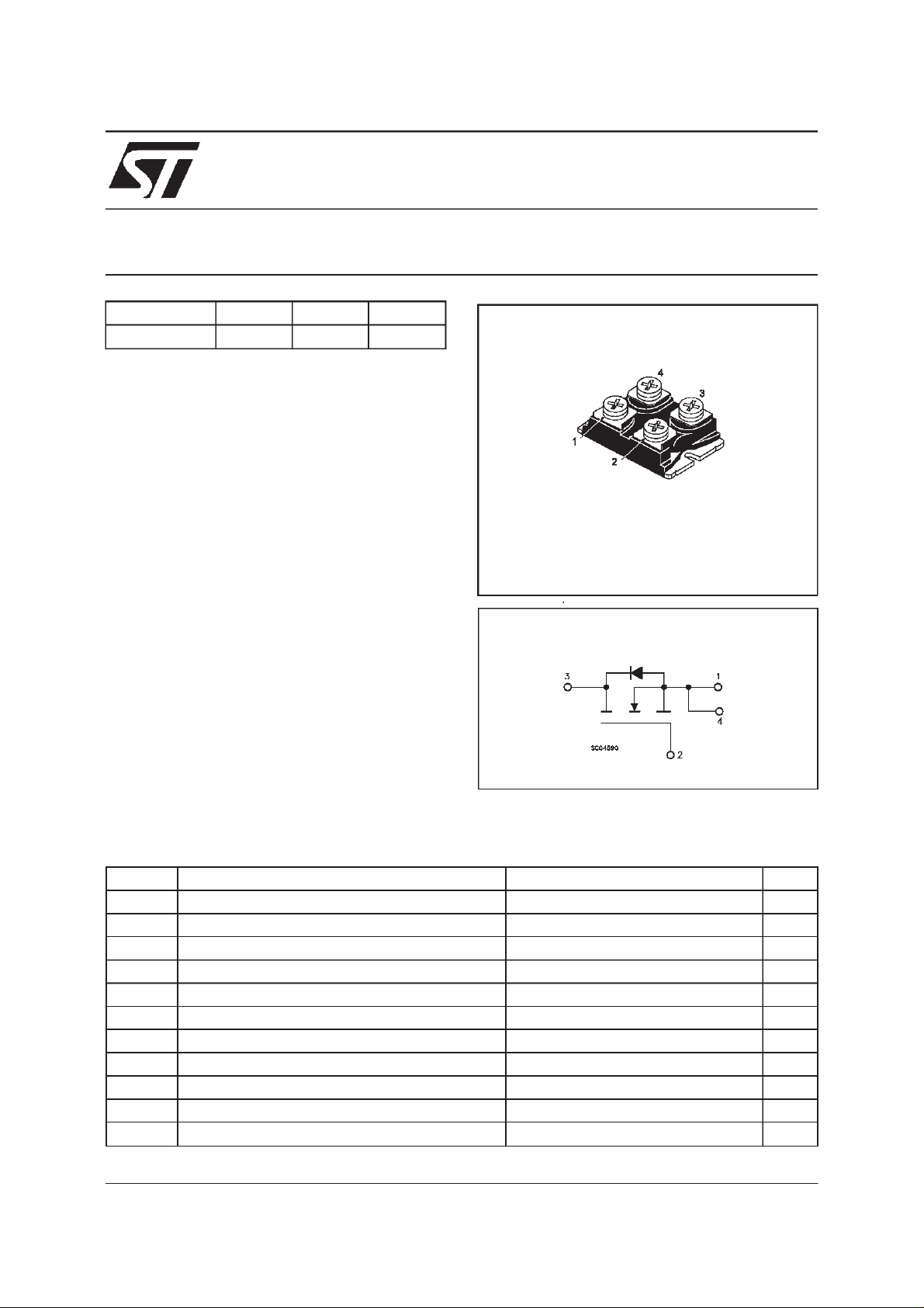
STE180N10
N - CHANNEL 100V - 5.5 mΩ - 180A - ISOTOP
POWER MOSFET
TYPE V
DSS
R
DS(on)
I
D
ST E180N10 100 V < 7 m Ω 180 A
■ TYPICALR
■ 100%AVALANCHETESTED
■ LOW INTRINSICCAPACITANCE
■ GATECHARGE MINIMIZED
■ REDUCEDVOLTAGESPREAD
DS(on)
= 5.5 mΩ
INDUSTRIAL APPLICATIONS:
■ SMPS& UPS
■ MOTORCONTROL
■ WELDINGEQUIPMENT
■ OUTPUTSTAGEFOR PWM, ULTRASONIC
CIRCUITS
ISOTOP
INTERNAL SCHEMATIC DIAGRAM
ABSOLUTE MAXIMUM RATINGS
Symb o l Parameter Value Unit
V
V
V
I
DM
P
V
T
(•) Pulse width limited by safe operating area (1)ISD≤
February 1999
Drain-source Volt age (VGS= 0) 100 V
DS
Drain- g at e Voltage (RGS=20kΩ) 100 V
DGR
Gate-s ource Voltage
GS
I
Drain Cur rent ( continuous ) at Tc=25oC 180 A
D
I
Drain Cur rent ( continuous ) at Tc=100oC 119 A
D
20 V
±
(•) Drain Cur rent ( pu ls ed) 540 A
Tot al Dissi pat ion at Tc=25oC 450 W
tot
Derat ing F ac tor 3.6 W/
Ins ulat i on Wi t hs t an d Voltage (AC -RMS) 2500 V
ISO
Sto rage Temperat ur e -55 to 15 0
stg
T
Max. Operating Junct ion Temperat ur e 150
j
180
Α,
di/dτ ≤ 200 A/µs, VDD≤ V
(BR)DSS,Tj≤TJMAX
o
C
o
C
o
C
1/8
Page 2
STE180N10
THERMAL DATA
R
thj-case
R
thc-h
AVALANCHE CHARACTERISTICS
Symbol Parameter Max Value Unit
I
AR
E
Ther mal Resistanc e Junct ion-case Max
Ther mal Resistanc e Case-heatsink W it h conduct ive
Gr ease Applied Max
Avalanche Current, R epetitive or Not-Repetitive
(pulse width limited by T
Single Pul se Avalanc he Ener gy
AS
(starting T
=25oC, ID=IAR,VDD=25V)
j
max)
j
0.27
0.05
60 A
720 mJ
o
C/W
o
C/W
ELECTRICAL CHARACTERISTICS
=25oC unless otherwisespecified)
(T
case
OFF
Symbol Parameter Test Condit ions Min. Typ. M ax. Unit
V
(BR)DSS
Drain-source
ID=1mA VGS= 0 100 V
Break dow n Vo lt age
I
DSS
I
GSS
Zero Gate Voltage
Drain Curre nt (V
GS
Gat e- bod y Leakag e
Current (V
DS
=0)
=0)
V
=MaxRating
DS
=MaxRating Tc= 125oC
V
DS
V
=± 20 V
GS
50
500
400 nA
±
ON(∗)
Symbol Parameter Test Condit ions Min. Typ. M ax. Unit
V
GS(th)
R
DS(on)
Gate Threshold Voltage VDS=VGSID= 250 µA 234V
Sta t ic Drain-s our c e On
VGS=10V ID=90A 5.5 7 m
Resistance
I
D(on)
On State Drain Current VDS>I
D(on)xRDS(on)max
180 A
VGS=10V
DYNAMIC
Symbol Parameter Test Condit ions Min. Typ. M ax. Unit
g
(∗)Forward
fs
Tr ansc on duc tance
C
C
C
Input Capaci t ance
iss
Out put Capac itance
oss
Reverse Transfer
rss
Capacit a nc e
VDS>I
D(on)xRDS(on)maxID
=90A 70 S
VDS=25V f=1MHz VGS=0 18
4
0.5
µ
µA
nF
nF
nF
A
Ω
2/8
Page 3
STE180N10
ELECTRICAL CHARACTERISTICS
(continued)
SWITCHING ON
Symbol Parameter Test Condit ions Min. Typ. M ax. Unit
t
d(on)
Tur n-on Delay Time
Rise Time
t
r
VDD=50V ID=90A
R
=4.7
G
Ω
VGS=10V
65
230
(Resis t iv e Load, see fig. 3 )
Q
Q
Q
Tot al Gate Charge
g
Gat e- Source Charge
gs
Gate-Drain Charge
gd
VDD=80V ID=180A VGS= 10 V 485
90
210
680 nC
SWITCHING OFF
Symbol Parameter Test Condit ions Min. Typ. M ax. Unit
t
d(on)
Tur n-of f Dela y Tim e
t
Fall T ime
r
VDD=50V ID=90A
=4.7 Ω VGS=10V
R
G
280
100
(Resis t iv e Load, see fig. 3 )
t
r(Voff)
t
t
Off-voltage Rise Time
Fall T ime
f
Cross-over Tim e
c
VDD=80V ID=180A
=4.7 Ω VGS=10V
R
G
(Indu ct iv e Load, see fig. 5)
100
170
260
SOURCEDRAINDIODE
Symbol Parameter Test Condit ions Min. Typ. M ax. Unit
I
SDM
V
I
SD
Q
I
RRM
SD
t
Source-drain Current
(•)
Source-drain Current
180
540
(pulsed)
(∗)ForwardOnVoltage ISD= 180 A VGS=0 1.5 V
Reverse Recovery
rr
Time
Reverse Recovery
rr
ISD= 180 A di/ d t = 100 A/µs
=50V Tj= 150oC
V
DD
(see test circuit, fig. 5)
250
1875
Charge
Reverse Recovery
15
Current
ns
ns
nC
nC
ns
ns
ns
ns
ns
A
A
ns
µC
A
(∗) Pulsed: Pulse duration = 300 µs, duty cycle 1.5 %
(•) Pulse width limited by safe operating area
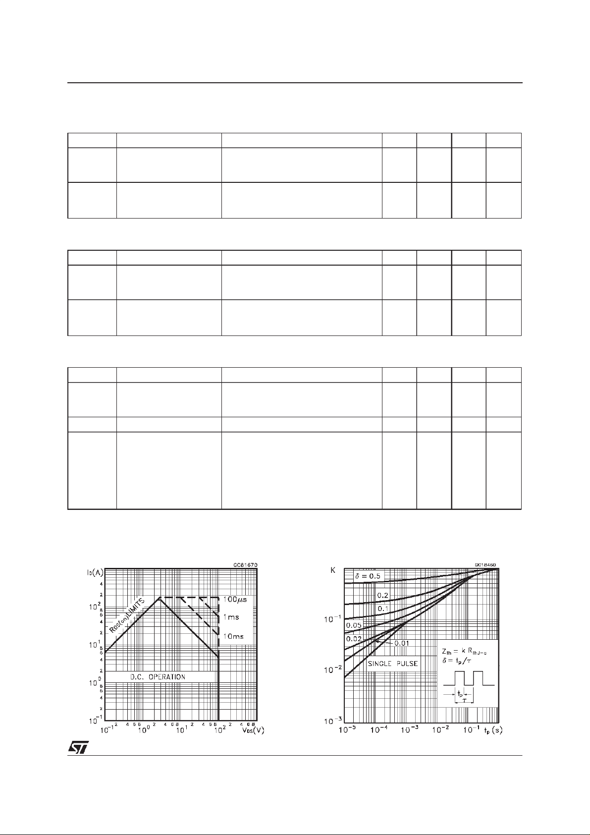
SafeOperating Area ThermalImpedance
3/8
Page 4

STE180N10
OutputCharacteristics
Transconductance
TransferCharacteristics
Static Drain-sourceOn Resistance
Gate Charge vs Gate-sourceVoltage
4/8
CapacitanceVariations
Page 5

STE180N10
NormalizedGate Threshold Voltage vs
Temperature
Source-drainDiode Forward Characteristics
NormalizedOn Resistancevs Temperature
5/8
Page 6

STE180N10
Fig. 1:
UnclampedInductiveLoad Test Circuit
Fig. 3: Switching Times Test CircuitsFor
ResistiveLoad
Fig. 2:
UnclampedInductive Waveform
Fig. 4: GateChargetest Circuit
Fig. 5:
Test CircuitFor InductiveLoad Switching
And Diode Recovery Times
6/8
Page 7

ISOTOPMECHANICALDATA
STE180N10
DIM.
MIN. TYP. MAX. MIN. TYP. MAX.
A 11.8 12.2 0.466 0.480
B 8.9 9.1 0.350 0.358
C 1.95 2.05 0.076 0.080
D 0.75 0.85 0.029 0.033
E 12.6 12.8 0.496 0.503
F 25.15 25.5 0.990 1.003
G 31.5 31.7 1.240 1.248
H 4 0.157
J 4.1 4.3 0.161 0.169
K 14.9 15.1 0.586 0.594
L 30.1 30.3 1.185 1.193
M 37.8 38.2 1.488 1.503
N 4 0.157
O 7.8 8.2 0.307 0.322
mm inch
G
A
B
O
N
D
E
F
H
J
C
K
L
M
7/8
Page 8

STE180N10
Information furnishedis believed tobeaccurate and reliable. However, STMicroelectronics assumes no responsibilityfor the consequences
of use of such information nor for any infringement of patents or other rights of third parties which may result from its use. No license is
granted by implication or otherwise under any patent or patent rights of STMicroelectronics. Specificationmentioned in this publicationare
subjecttochange without notice. This publication supersedes andreplaces all information previously supplied.STMicroelectronicsproducts
are not authorized for useas critical components in life support devicesor systemswithout express written approval of STMicroelectronics.
The ST logo is a trademark of STMicroelectronics
1999 STMicroelectronics – Printed in Italy – All Rights Reserved
STMicroelectronics GROUP OF COMPANIES
Australia - Brazil - Canada - China - France - Germany - Italy - Japan - Korea - Malaysia - Malta - Mexico - Morocco - The Netherlands -
8/8
Singapore - Spain - Sweden - Switzerland - Taiwan - Thailand - United Kingdom - U.S.A.
http://www.st.com
.
 Loading...