

Page 1
®
LOW CAPACITANCE DETECTION DIODE
MAIN PRODUCT CHARACTERISTICS
STDD15 series
I
F(AV)
V
RRM
10 mA
15 V
Tj (max) 150 °C
(max) 0.51 V
V
F
FEATURES AND BENEFITS
Low diode capacitance
■
Device designed for RF application
■
Low profile package
■
Available in 3 configurations
■
■ Very low parasitic inductor & resistor
DESCRIPTION
The STDD15 is a dual diode series for the
detection of a RF signal and the compensation of
thevoltagedriftwiththe temperature. TheSOT323
package makes the device ideal in application
where the space saving is critical like mobile
phones.
The low junction capacitance will reduce the
disturbance on the RF signal
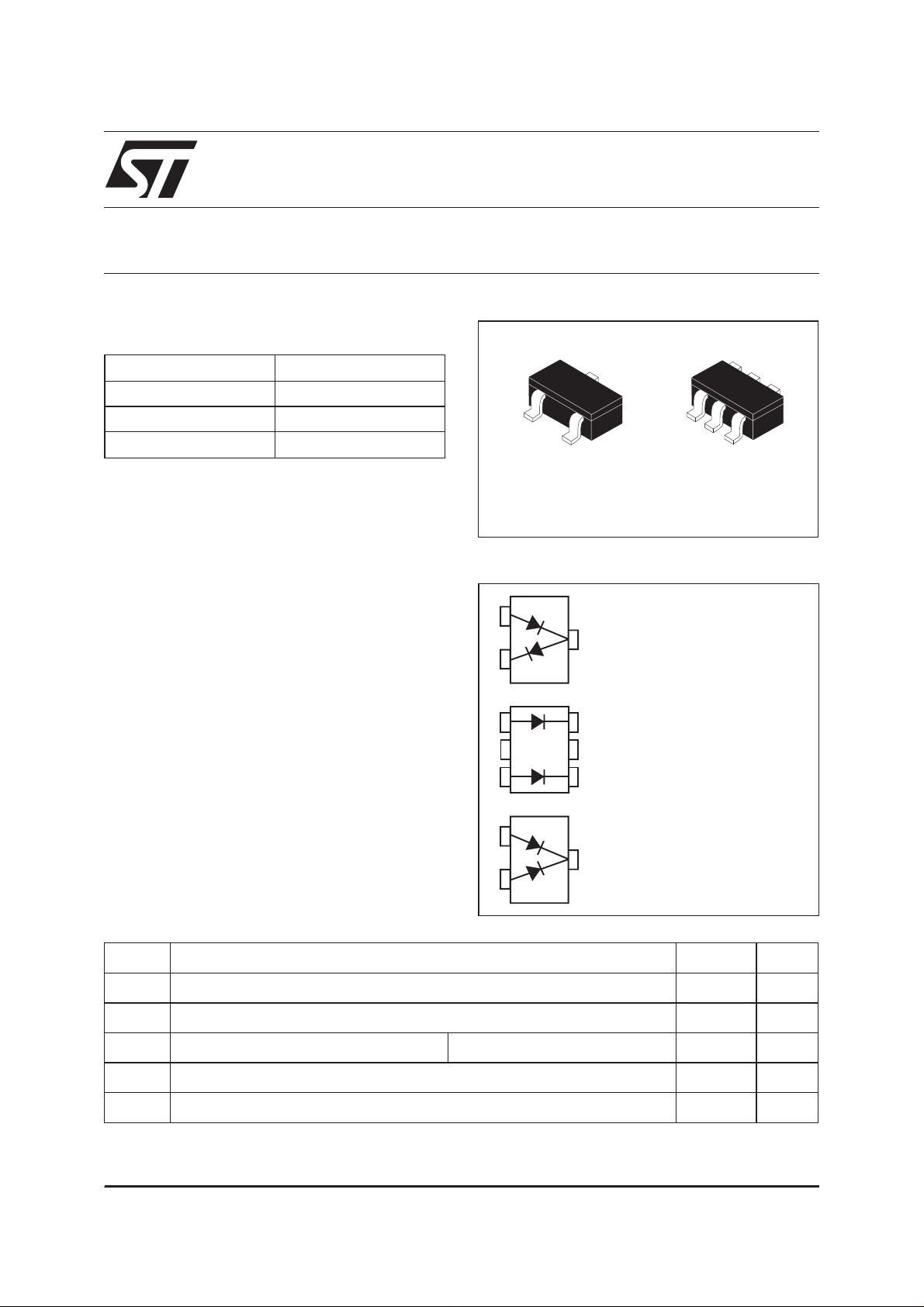
SOT323-3L
STDD15-xxW
SCHEMATIC DIAGRAM
1
3
2
1
2
3
4
5
6
SOT323-6L
STDD15-xxS
Series configuration
STDD15-04W
Parallel configuration
STDD15-07S
1
3
2
Common cathode configuration
STDD15-05W
ABSOLUTE RATINGS (limiting values)
Symbol Parameter Value Unit
V
RRM
I
FSM
T
I
stg
Repetitive peak reverse voltage 15 V
Continuous forward current 10 mA
F
Surge non repetitive forward current tp = 10ms 2 A
Storage temperature range - 65 + 150 °C
Tj Maximum operating junction temperature 150 °C
August 2002 - Ed: 3A
1/6
Page 2
STDD15 series
THERMAL PARAMETERS
Symbol Parameter Value Unit
R
* Junctionto ambient 500 °C/W
th (j-a)
*: Mounted with minimum recommended pad size, PC board FR4.
STATIC ELECTRICAL CHARACTERISTICS
Symbol Parameter Tests conditions Min. Typ. Max. Unit
I
* Reverse leakage
R
current
Tj = 25°C V
= 1V 0.035 µA
R
Tj = 125°C 6 30
Tj = 25°C V
= 15V 0.23 µA
R
Tj = 125°C 10 100
V
* Forward voltage drop Tj = 25°C I
F
= 1 mA 350 380 mV
F
Tj = 125°C 230 260
Tj = 25°C I
= 10 mA 500 570
F
Tj = 125°C 450 510
* Pulse test: tp ≤ 250µs, Delta ≤ 2%
ELECTRICAL CHARACTERISTICS
Symbol Parameter Tests conditions Min. Typ. Max. Unit
C Diode capacitance V
R
F
Forward resistance IF= 5 mA F = 100MHz 15 Ω
= 0 V F = 1MHz 1.0 pF
R
Ls Series inductance 1.5 nH
2/7
Page 3

STDD15 series
Fig. 1: Forward voltage drop versus forward
current (typical values).
IFM(mA)
1.E+02
1.E+01
Tj=125°CTj=125°C
1.E+00
1.E-01
0.0 0.2 0.4 0.6 0.8 1.0 1.2
Tj=85°CTj=85°C
Tj=25°CTj=25°C
Tj=-40°CTj=-40°C
VFM(V)
Fig. 3: Differential forward resistance versus
forward current (typical values).
RF( )Ω
100
10
IF(mA)
1
1.0 10.0 100.0
F=10kHz
Tj=25°C
Fig. 2: Reverse leakage current versus reverse
voltage applied (typical values).
IR(µA)
1.E+02
1.E+01
1.E+00
1.E-01
1.E-02
1.E-03
0.0 2.5 5.0 7.5 10.0 12.5 15.0
Tj=125°C
Tj=85°C
Tj=25°C
VR(V)
Fig. 4: Junction capacitance versus reverse
voltage applied (typical values).
C(pF)
1.0
0.9
0.8
0.7
0.6
0.5
0.4
0.3
0.2
0.1
0.0
0.0 2.5 5.0 7.5 10.0 12.5 15.0
VR(V)
F=1MHz
Vosc=30mV
Tj=25°C
RMS
Fig. 5: Variation of thermal impedance junction to
ambient versus pulse duration (printed circuit
board, epoxy FR4).
Zth(j-a)(°C/W)
1000.0
100.0
tp(s)
10.0
1.E-02 1.E-01 1.E+00 1.E+01 1.E+02
Fig. 6: Thermal resistance junction to ambient
versus copper surface under each lead (printed
circuit board, epoxy FR4)..
Rth(j-a)
600
550
500
450
400
350
S(mm²)
300
0 5 10 15 20 25 30 35 40 45 50
3/6
Page 4

STDD15 series
Electrical Model (PSPICE)
Parameter Value Unit
Is 2.66 e-8 A
N 1.04
M 0.772
Vj 0.65 V
Eg 0.69 eV
Xti 2
Rs 15 W
Cjo 0.85e-12 F
Bv 20 V
Ibv 10 e-3 A
PACKAGE MECHANICAL DATA
SOT323-3L
A
REF.
DIMENSIONS
Millimeters Inches
A1
L
H
θ
c
FOOTPRINT (in millimeters)
0.95
Min. Typ. Max. Min. Typ. Max.
A 0.8 1.1 0.031 0.043
D
A1 0.0 0.1 0.0 0.004
b 0.25 0.4 0.010 0.016
b
c 0.1 0.26 0.004 0.010
D 1.8 2.0 2.2 0.071 0.079 0.086
E 1.15 1.25 1.35 0.045 0.049 0.053
E
e 0.65 0.026
H 1.8 2.1 2.4 0.071 0.083 0.094
L 0.1 0.2 0.3 0.004 0.008 0.012
e
2.9
1
θ 0 30° 0 30°
4/6
0.8
0.50
Page 5

PACKAGE MECHANICAL DATA
SOT323-6L
A
A1
D
L
HE
Q1
c
b
STDD15 series
DIMENSIONS
A2
ee
E
REF.
Millimeters Inches
Min. Max. Min. Max.
A 0.8 1.1 0.031 0.043
A1 0 0.1 0 0.004
A2 0.8 1 0.031 0.039
b 0.15 0.3 0.006 0.012
c 0.1 0.18 0.004 0.007
D 1.8 2.2 0.071 0.086
E 1.15 1.35 0.045 0.053
e 0.65 Typ. 0.025 Typ.
HE 1.8 2.4 0.071 0.094
Q1 0.1 0.4 0.004 0.016
L 0.1 0.45 0.004 0.018
FOOTPRINT (in millimeters)
0.3mm
1mm
2.9mm
1mm
0.35mm
Note: The device fulfills the MSL level 1 after
leadfree soldering profile.
Ordering code Marking Package Weight Base qty Delivery mode
STDD15-04W 24 SOT323-3L 0.006 g 3000 Tape & reel
STDD15-05W 25 SOT323-3L 0.006 g 3000 Tape & reel
STDD15-07S D25 SOT323-6L 0.006 g 3000 Tape & reel
5/6
Page 6

STDD15 series
Informationfurnishedisbelieved to be accurate and reliable. However, STMicroelectronics assumes no responsibility for the consequences of
useof such information nor for any infringement of patents or otherrightsof third parties which may result from its use. No licenseis granted by
implication or otherwise under any patent or patent rights of STMicroelectronics. Specifications mentioned in this publication are subject to
change without notice. This publication supersedes and replaces all information previously supplied.
STMicroelectronics products are not authorized for use as critical components in life support devices or systems without express written approval of STMicroelectronics.
The ST logo is a registered trademark of STMicroelectronics
© 2002 STMicroelectronics - Printed in Italy - All rights reserved.
STMicroelectronics GROUP OF COMPANIES
Australia - Brazil - Canada - China - Finland - France - Germany
Hong Kong - India - Israel - Italy - Japan - Malaysia - Malta - Morocco - Singapore
Spain - Sweden - Switzerland - United Kingdom - United States.
http://www.st.com
6/6
 Loading...