

Page 1
STD9N10
N - CHANNEL ENHANCEMENT MODE
POWER MOS TRANSISTOR
TYPE V
DSS
R
DS(on)
I
D
STD9N10 100 V < 0.27 Ω 9A
■ TYPICALR
■ AVALANCHERUGGEDTECHNOLOGY
■ 100% AVALANCHETESTED
■ REPETITIVEAVALANCHEDATAAT 100
■ LOW GATE CHARGE
■ HIGH CURRENTCAPABILITY
o
■ 175
■ APPLICATIONORIENTED
COPERATINGTEMPERATURE
DS(on)
=0.23 Ω
o
C
CHARACTERIZATION
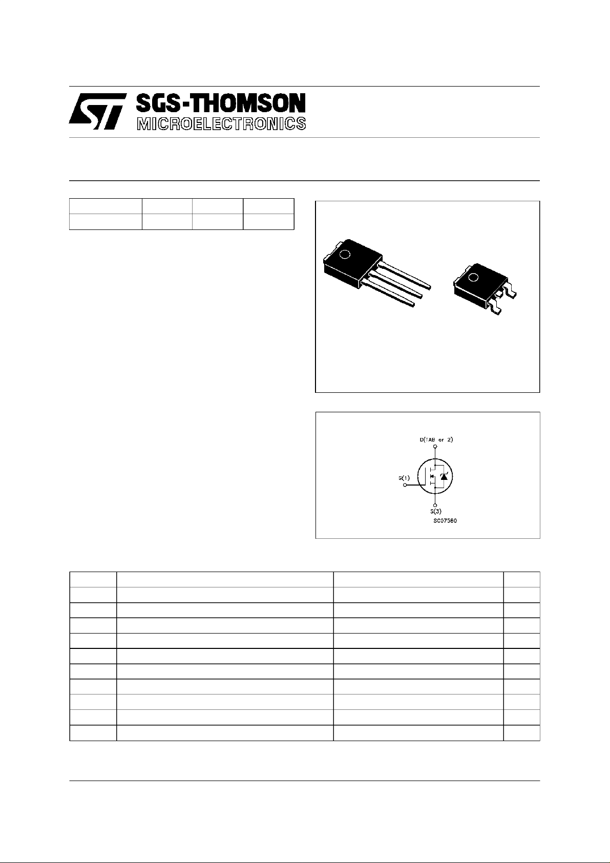
■ THROUGH-HOLE IPAK (TO-251) POWER
PACKAGEIN TUBE(SUFFIX ”-1”)
■ SURFACE-MOUNTINGDPAK (TO-252)
POWERPACKAGE IN TAPE & REEL
(SUFFIX”T4”)
APPLICATIONS
■ HIGH CURRENT, HIGH SPEEDSWITCHING
■ SOLENOIDANDRELAY DRIVERS
■ REGULATORS
■ DC-DC& DC-AC CONVERTERS
■ MOTORCONTROL,AUDIO AMPLIFIERS
■ AUTOMOTIVEENVIRONMENT (INJECTION,
ABS, AIR-BAG,LAMPDRIVERS,Etc.)
3
2
IPAK
TO-251
(Suffix”-1”)
1
(Suffix ”T4”)
1
DPAK
TO-252
INTERNAL SCHEMATIC DIAGRAM
3
ABSOLUTE MAXIMUM RATINGS
Symb o l Parame t er Val u e Uni t
V
V
DGR
V
I
DM
P
T
(•) Pulse width limitedby safe operating area
March 1996
Drain-source Voltage (VGS= 0) 100 V
DS
Drain- gate Voltage (RGS=20kΩ) 100 V
Gate-source Voltage ± 20 V
GS
I
Drain Current (c ont inuo us) a t Tc=25oC9A
D
I
Drain Current (c ont inuo us) a t Tc=100oC6A
D
(•) Drain Current (puls ed) 36 A
Total Dissipat i on at Tc=25oC45W
tot
Derat ing Factor 0.3 W/
Stora ge Temperature -65 to 175
stg
T
Max. Operat ing Junction T emperatur e 175
j
o
o
o
C
C
C
1/10
Page 2
STD9N10
THERMAL DATA
R
thj-case
R
thj-amb
R
thc-sin k
T
AVALANCHE CHARACTERISTICS
Symb o l Para met er Max V alue Uni t
I
AR
E
E
I
AR
Ther mal Resistance Junct ion-case Max
Ther mal Resistance Junct ion-ambient Max
Ther mal Resistance Case-s i nk Typ
Maximum Lead Tempera t ure For Solder ing Purpo se
l
Avalanche Current , Repet it iv e or Not-Repe t it ive
(pulse width limit ed by T
Single Pu lse Avalanc he E nerg y
AS
(starti ng T
Repetitive Avalanche E n er gy
AR
=25oC, ID=IAR,VDD=25V)
j
(pulse width limit ed by T
max, δ <1%)
j
max, δ <1%)
j
Avalanche Current , Repet it iv e or Not-Repe t it ive
=100oC, pulse wid t h limited by Tjmax, δ <1%)
(T
c
3.33
100
1.5
275
9A
30 mJ
7mJ
6A
o
C/W
o
C/W
o
C/W
o
C
ELECTRICAL CHARACTERISTICS (T
=25oC unlessotherwise specified)
case
OFF
Symbol Parameter Test Conditions Min. Typ. Max. Unit
V
(BR)DSS
Drain-source
ID= 250 µAVGS= 0 100 V
Break dow n Voltage
I
I
DSS
GSS
Zero Gate Voltage
Drain Current (V
GS
Gat e- bod y Leaka ge
Current (V
DS
=0)
=0)
=MaxRating
V
DS
V
=MaxRatingx0.8 Tc= 125oC
DS
V
= ± 20 V ± 100 nA
GS
250
1000µAµA
ON (∗)
Symbol Parameter Test Conditions Min. Typ. Max. Unit
V
GS(th )
R
DS(on)
I
D(on)
Gat e Thres hold Volt age VDS=VGSID=250µA234V
St at ic Drain-source On
Resistance
VGS= 10V ID=4.5A
= 10V ID=4.5A Tc=100oC
V
GS
On S t ate Drain Current VDS>I
D(on)xRDS(on)max
0.23 0.27
0.54
9A
VGS=10V
DYNAMIC
Symbol Parameter Test Conditions Min. Typ. Max. Unit
g
(∗)Forward
fs
Tr ansc on ductance
C
C
C
Input Capac it an ce
iss
Out put Capac itance
oss
Reverse Transfer
rss
Capacit a nc e
VDS>I
D(on)xRDS(on)maxID
=4.5A 2 4 S
VDS=25V f=1MHz VGS= 0 330
90
25
450
120
40
Ω
Ω
pF
pF
pF
2/10
Page 3
STD9N10
ELECTRICAL CHARACTERISTICS (continued)
SWITCHINGON
Symbol Parameter Test Conditions Min. Typ. Max. Unit
t
d(on)
t
r
Turn-on Time
Rise Time
VDD=50V ID=4.5A
=4.7 Ω VGS=10V
R
G
(see t est circuit, figure 3)
(di/dt)
Tur n-on C urr ent Slope VDD=80V ID=9A
on
R
=4.7 Ω VGS=10V
G
(see t est circuit, figure 5)
Q
Q
Q
Tot al Gat e Charge
g
Gate-Source Charge
gs
Gat e- Drain Charge
gd
VDD=80V ID=9A VGS=10V 15
SWITCHINGOFF
Symbol Parameter Test Conditions Min. Typ. Max. Unit
t
r(Voff)
t
Off -voltage R ise T ime
t
Fall T ime
f
Cross-over Time
c
VDD=80V ID=9A
=4.7 Ω VGS=10V
R
G
(see t est circuit, figure 5)
SOURCE DRAIN DIODE
10
40
15
60
440 A / µ s
25 nC
6
5
15
25
50
25
35
70
ns
ns
nC
nC
ns
ns
ns
Symbol Parameter Test Conditions Min. Typ. Max. Unit
I
I
SDM
SD
Source-drain Current
(•)
Source-drain Current
9
36
(pulsed)
(∗)ForwardOnVoltage ISD=9A VGS=0 1.5 V
V
SD
t
Q
Reverse Recovery
rr
Time
Reverse Recovery
rr
ISD= 9 A di/ dt = 100 A/µs
=20V Tj= 150oC
V
DD
(see t est circuit, figure 5)
80
0.2
Charge
I
RRM
Reverse Recovery
5
Current
(∗) Pulsed: Pulse duration =300 µs, duty cycle 1.5 %
(•) Pulse width limited by safeoperating area
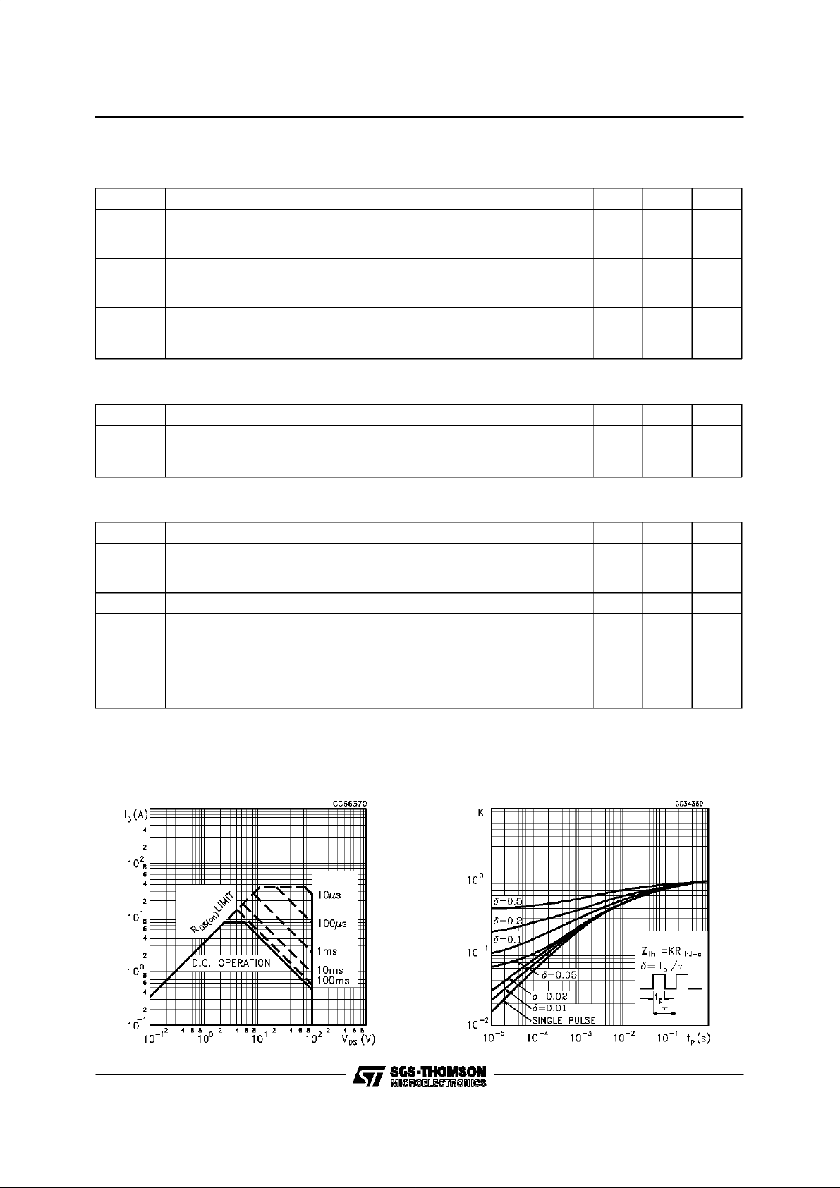
Safe Operating Area ThermalImpedance
A
A
ns
µC
A
3/10
Page 4

STD9N10
Derating Curve
TransferCharacteristics
OutputCharacteristics
Transconductance
StaticDrain-source On Resistance
4/10
Gate Charge vs Gate-sourceVoltage
Page 5

STD9N10
CapacitanceVariations
Normalized OnResistance vs Temperature
Normalized GateThreshold Voltagevs
Temperature
Turn-onCurrent Slope
Turn-offDrain-source VoltageSlope
Cross-overTime
5/10
Page 6

STD9N10
SwitchingSafe Operating Area
Source-drainDiode Forward Characteristics
AccidentalOverload Area
Fig. 1: UnclampedInductive Load Test Circuit
6/10
Fig. 2: UnclampedInductiveWaveform
Page 7

STD9N10
Fig. 3: SwitchingTimes Test Circuits For
ResistiveLoad
Fig. 5: Test Circuit For InductiveLoad Switching
And DIodeRecovery Times
Fig. 4: GateCharge test Circuit
7/10
Page 8

STD9N10
TO-251 (IPAK) MECHANICAL DATA
DIM.
mm inch
MIN. TYP. MAX. MIN. TYP. MAX.
A 2.2 2.4 0.086 0.094
A1 0.9 1.1 0.035 0.043
A3 0.7 1.3 0.027 0.051
B 0.64 0.9 0.025 0.031
B2 5.2 5.4 0.204 0.212
B3 0.85 0.033
B5 0.3 0.012
B6 0.95 0.037
C 0.45 0.6 0.017 0.023
C2 0.48 0.6 0.019 0.023
D 6 6.2 0.236 0.244
E 6.4 6.6 0.252 0.260
G 4.4 4.6 0.173 0.181
H 15.9 16.3 0.626 0.641
L 9 9.4 0.354 0.370
L1 0.8 1.2 0.031 0.047
L2 0.8 1 0.031 0.039
8/10
A
E
==
C2
L2
B2
==
H
C
A3
A1
B6
L
B
B5
G
==
D
B3
2
13
L1
0068771-E
Page 9

TO-252 (DPAK) MECHANICALDATA
STD9N10
DIM.
mm inch
MIN. TYP. MAX. MIN. TYP. MAX.
A 2.2 2.4 0.086 0.094
A1 0.9 1.1 0.035 0.043
A2 0.03 0.23 0.001 0.009
B 0.64 0.9 0.025 0.035
B2 5.2 5.4 0.204 0.212
C 0.45 0.6 0.017 0.023
C2 0.48 0.6 0.019 0.023
D 6 6.2 0.236 0.244
E 6.4 6.6 0.252 0.260
G 4.4 4.6 0.173 0.181
H 9.35 10.1 0.368 0.397
L2 0.8 0.031
L4 0.6 1 0.023 0.039
H
A
E
==
C2
L2
B2
==
DETAIL”A”
D
2
13
L4
A1
C
A2
DETAIL”A”
B
G
==
0068772-B
9/10
Page 10

STD9N10
Information furnished is believedto be accurate and reliable. However, SGS-THOMSONMicroelectronics assumes no responsability for the
consequencesof use ofsuch information nor for any infringement of patents or otherrights of third parties which may resultsfrom its use. No
licenseis grantedby implicationor otherwise underany patentor patentrights ofSGS-THOMSONMicroelectronics. Specificationsmentioned
in this publicationare subjectto change without notice. This publication supersedes and replaces all information previously supplied.
SGS-THOMSONMicroelectronics productsarenotauthorized for useas critical components in lifesupportdevicesor systems withoutexpress
writtenapproval of SGS-THOMSONMicroelectonics.
1995 SGS-THOMSONMicroelectronics - All Rights Reserved
Australia - Brazil- France - Germany - HongKong - Italy - Japan - Korea - Malaysia - Malta - Morocco- TheNetherlands -
Singapore- Spain- Sweden- Switzerland- Taiwan - Thailand - United Kingdom - U.S.A
SGS-THOMSONMicroelectronicsGROUPOF COMPANIES
...
10/10
 Loading...