

Page 1
STD7NB20
N - CHANNEL ENHANCEMENT MODE
PowerMESH MOSFET
■ TYPICALR
DS(on)
=0.3Ω
■ EXTREMELY HIGH dv/dt CAPABILITY
■ 100% AVALANCHETESTED
■ VERYLOW INTRINSIC CAPACITANCES
■ GATECHARGEMINIMIZED
■ FOR TROUGH-HOLE VERSIONCONTACT
SALESOFFICE
DESCRIPTION
Using the latest high voltage MESH OVERLAY
process, SGS-Thomson has designed an
advanced family of power MOSFETs with
outstanding performances. The new patent
pending strip layout coupled with the Company’s
proprietary edge termination structure, gives the
lowest R
DS(on)
per area, exceptional avalanche
and dv/dt capabilities and unrivalled gate charge
and switching characteristics.
APPLICATIONS
■ SWITCHMODEPOWER SUPPLIES(SMPS)
■ DC-ACCONVERTERS FOR WELDING
EQUIPMENTAND UNINTERRUPTIBLE
POWERSUPPLIESAND MOTORDRIVE
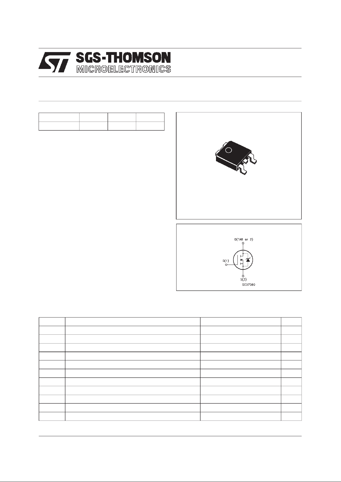
INTERNAL SCHEMATIC DIAGRAM
December 1997
1
3
DPAK
TO-252
(Suffix ”T4”)
ABSOLUTE MAXIMUM RATINGS
Symb o l Para meter Value Uni t
V
DS
Drain-source Voltage (VGS=0) 200 V
V
DGR
Drain- gate Voltage (RGS=20kΩ)
200 V
V
GS
Gat e- source Vo lt age ± 30 V
I
D
Drain Cur rent ( contin uous ) a t Tc=25oC7A
I
D
Drain Cur rent ( contin uous ) a t Tc=100oC5A
I
DM
(•) Dra in Cur rent ( pul s ed ) 28 A
P
tot
Tot al Dissipation at Tc=25oC55W
Derating Factor 0.44 W/
o
C
dv/dt(
1) Peak Diode Re covery vo ltage slope 5.5 V/ns
T
stg
Sto rage Tempe rature -65 to 150
o
C
T
j
Max. Operatin g Ju nct ion T e m peratur e 150
o
C
(•) Pulse width limited by safe operating area (1)ISD≤7A, di/dt ≤ 200 A/µs, VDD≤ V
(BR)DSS
,Tj≤T
JMAX
TYPE V
DSS
R
DS(on)
I
D
ST D7 NB20 200 V < 0. 4 0 Ω 7A
1/8
Page 2
THERMAL DATA
R
thj-case
Rthj-a mb
R
thc-sin k
T
l
Ther mal Resist ance Junctio n-c a s e Max
Ther mal Resist ance Junctio n-ambient Max
Ther mal Resist ance Case-sink T yp
Maximum Lead Temperat ure For Soldering Purpose
2.27
100
1.5
275
o
C/W
oC/W
o
C/W
o
C
AVALANCHE CHARACTERISTICS
Symbol Para met e r Max Value Uni t
I
AR
Avalanche C urr e nt , Rep et it ive or Not-Re petitive
(pulse width limited by T
j
max, δ <1%)
7A
E
AS
Single Pulse Avalanche Energy
(starting T
j
=25oC, ID=IAR,VDD=50V)
100 mJ
ELECTRICAL CHARACTERISTICS (T
case
=25oC unlessotherwisespecified)
OFF
Symbol Parameter Test Cond itions Min. Typ. Ma x. Unit
V
(BR)DSS
Drain-sourc e
Breakdown V oltage
I
D
=250µAVGS=0
200 V
I
DSS
Zer o Gat e V o lt age
Drain Current (V
GS
=0)
V
DS
=MaxRating
V
DS
=MaxRating Tc=125oC
1
10
µA
µA
I
GSS
Gat e-body Leaka ge
Current (V
DS
=0)
V
GS
= ± 30 V
± 100 nA
ON (∗)
Symbol Parameter Test Cond itions Min. Typ. Ma x. Unit
V
GS(th )
Gate Threshold
Voltage
V
DS=VGSID
=250µA
345V
R
DS(on)
Stati c D rain-source On
Resistance
VGS=10V ID=3.5 A 0.30 0.40 Ω
I
D(on)
On State Drain Current VDS>I
D(on)xRDS(on)max
VGS=10V
7A
DYNAMIC
Symbol Parameter Test Cond itions Min. Typ. Ma x. Unit
g
fs
(∗)Forward
Tr ansconductanc e
VDS>I
D(on)xRDS(on)maxID
=3.5 A 2 3 S
C
iss
C
oss
C
rss
Input Capac i t an c e
Out put C apa c itance
Reverse Transf er
Capa cit an c e
VDS=25V f=1MHz VGS= 0 470
135
22
650
190
30
pF
pF
pF
STD7NB20
2/8
Page 3
ELECTRICAL CHARACTERISTICS (continued)
SWITCHINGON
Symbol Parameter Test Cond itions Min. Typ. Ma x. Unit
t
d(on)
t
r
Turn-on Time
Rise Time
VDD=100V ID=5A
R
G
=4.7 Ω VGS=10V
(see test circuit, figure 3)
10
15
14
20
ns
ns
Q
g
Q
gs
Q
gd
Total Gate Charge
Gat e-Sour ce Cha rge
Gate-Drain Charge
VDD=160V ID=10 A VGS=10V 17
7.5
5.5
24 nC
nC
nC
SWITCHINGOFF
Symbol Parameter Test Cond itions Min. Typ. Ma x. Unit
t
r(Voff)
t
f
t
c
Of f - voltag e Rise Time
Fall Time
Cross-ov er T im e
VDD=160V ID=10A
R
G
=4.7 Ω VGS=10V
(see test circuit, figure 5)
8
10
20
11
14
28
ns
ns
ns
SOURCE DRAIN DIODE
Symbol Parameter Test Cond itions Min. Typ. Ma x. Unit
I
SD
I
SDM
(•)
Source-drain Curre nt
Source-drain Curre nt
(pulsed)
7
28
A
A
V
SD
(∗) For ward On Vo lt age ISD=7A VGS=0 1.5 V
t
rr
Q
rr
I
RRM
Reverse Recovery
Time
Reverse Recovery
Charge
Reverse Recovery
Current
I
SD
= 10 A di/dt = 10 0 A/µs
V
DD
=50V Tj=150oC
(see test circuit, figure 5)
170
980
11.5
ns
nC
A
(∗) Pulsed: Pulseduration = 300 µs, duty cycle 1.5 %
(•) Pulse width limited by safe operating area
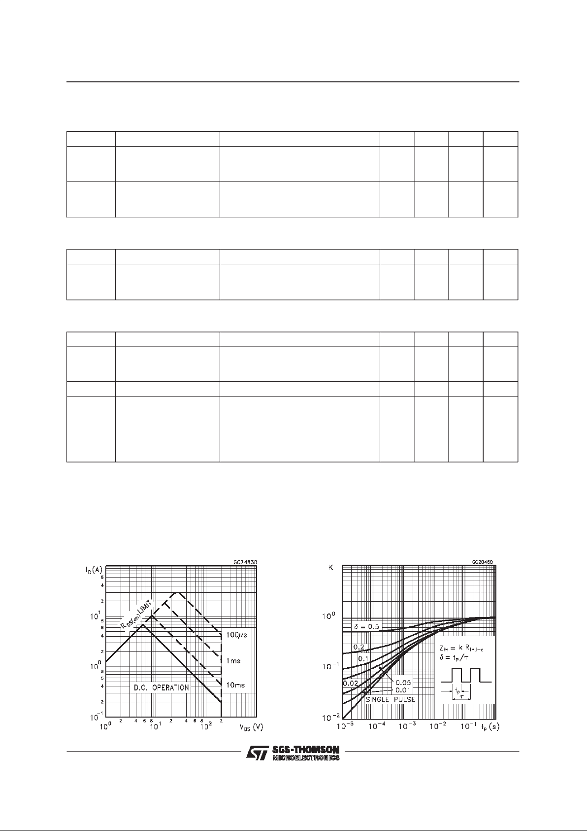
Safe Operating Area ThermalImpedance
STD7NB20
3/8
Page 4

OutputCharacteristics
Transconductance
GateCharge vs Gate-sourceVoltage
TransferCharacteristics
StaticDrain-sourceOn Resistance
CapacitanceVariations
STD7NB20
4/8
Page 5

Normalized Gate Threshold Voltage vs
Temperature
Source-drainDiode Forward Characteristics
Normalized On Resistance vs Temperature
STD7NB20
5/8
Page 6

Fig. 1: Unclamped Inductive Load TestCircuit
Fig. 3: SwitchingTimes Test CircuitsFor
ResistiveLoad
Fig. 2: Unclamped InductiveWaveform
Fig. 4: Gate Charge test Circuit
Fig. 5: Test Circuit For InductiveLoad Switching
And Diode RecoveryTimes
STD7NB20
6/8
Page 7

DIM.
mm inch
MIN. TYP. MAX. MIN. TYP. MAX.
A 2.2 2.4 0.086 0.094
A1 0.9 1.1 0.035 0.043
A2 0.03 0.23 0.001 0.009
B 0.64 0.9 0.025 0.035
B2 5.2 5.4 0.204 0.212
C 0.45 0.6 0.017 0.023
C2 0.48 0.6 0.019 0.023
D 6 6.2 0.236 0.244
E 6.4 6.6 0.252 0.260
G 4.4 4.6 0.173 0.181
H 9.35 10.1 0.368 0.397
L2 0.8 0.031
L4 0.6 1 0.023 0.039
==
D
L2
L4
13
==
B
E
==
B2
G
2
A
C2
C
H
A1
DETAIL”A”
A2
DETAIL”A”
TO-252 (DPAK) MECHANICAL DATA
0068772-B
STD7NB20
7/8
Page 8

Information furnished is believed tobe accurate and reliable. However,SGS-THOMSON Microelectronicsassumesno responsability forthe
consequencesof use ofsuch information nor for anyinfringement of patents or otherrights of third parties which may resultsfrom its use. No
licenseis granted by implicationor otherwise under any patent or patentrights ofSGS-THOMSONMicroelectronics.Specificationsmentioned
in this publicationare subjectto change without notice.This publication supersedes andreplaces all information previouslysupplied.
SGS-THOMSONMicroelectronics products arenotauthorizedforuseas criticalcomponents in lifesupportdevices or systemswithoutexpress
writtenapproval of SGS-THOMSONMicroelectonics.
1997 SGS-THOMSONMicroelectronics- Printedin Italy - AllRights Reserved
SGS-THOMSONMicroelectronics GROUP OF COMPANIES
Australia- Brazil - Canada- China- France- Germany - Italy- Japan -Korea - Malaysia- Malta- Morocco - The Netherlands-
Singapore- Spain- Sweden- Switzerland- Taiwan - Thailand - United Kingdom- U.S.A
...
STD7NB20
8/8
 Loading...