

Page 1
STD6NF10
N-CHANNEL 100V - 0.22 Ω - 6A IPAK/DPAK
LOW GATE CHARGE STripFET™ POWER MOSFET
TYPE
V
DSS
STD6NF10 100 V <0.250
■ TYPICAL R
■ EXCEPTIONA L dv/d t CAPABILITY
■ 100% AVALANCHE TESTED
■ LOW THRESHOLD DRIVE
■ THROUGH-HOLE IPAK (TO-251) POWER
(on) = 0.22 Ω
DS
R
DS(on)
I
D
6 A
Ω
PACKAGE IN TUBE (SUFFIX “- 1 ")
■ SURFACE-MOUNTING DPAK (TO-252)
POWER PACKAGE IN TAPE & REEL
(SUFFIX “T4")
DESCRIPTION
This MOSFET series realized with STMicroelectronics
unique STripFET process has specifically been designed
to minimize input capacitance and gate charge. It is
therefore suitable as primary switch in advanced highefficiency, high-frequency isolated DC-DC converters for
Telecom and Computer applications. It is also intended
for any applications with low gate drive requirements.
APPLICATIONS
■ HIGH-EFFICIENCY DC-DC CONVERTERS
■ UPS AND MOTOR CONTROL
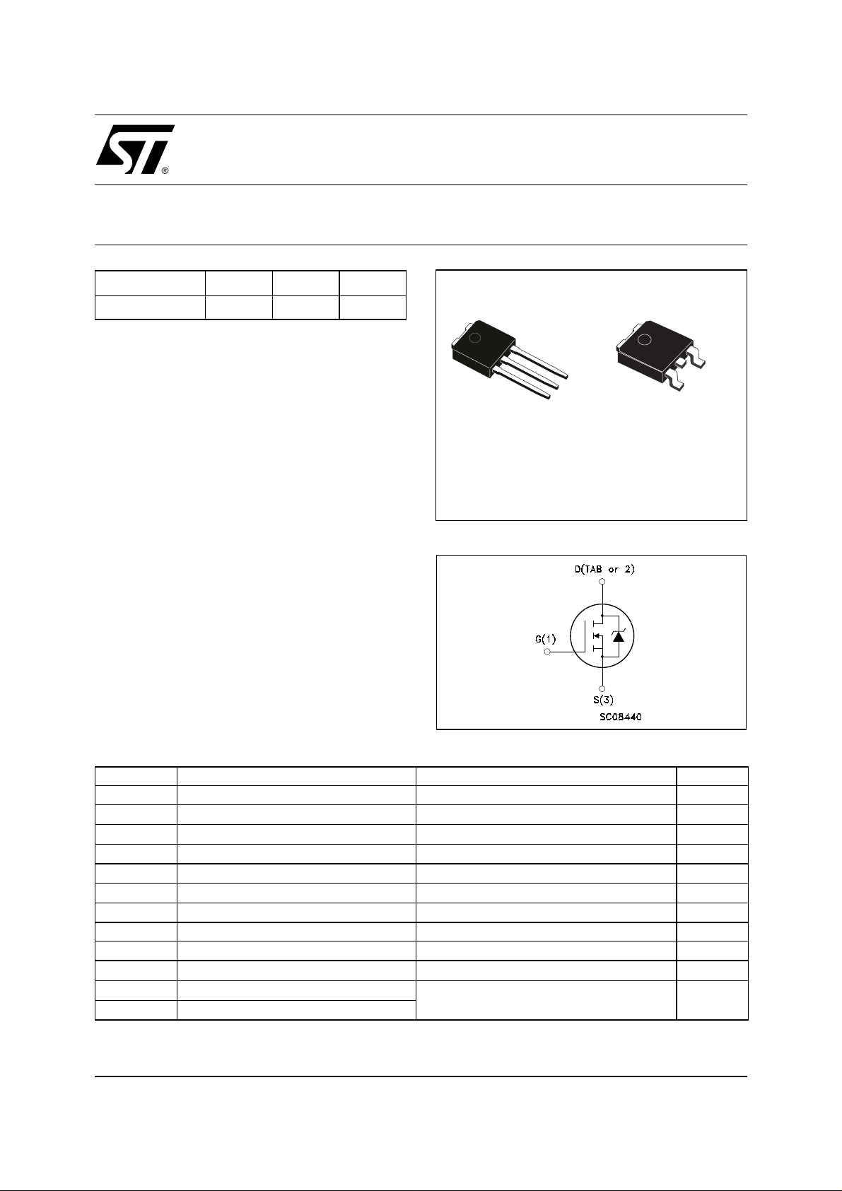
3
2
1
IP AK
TO-251
(Suffix “-1”)
DPAK
TO-252
(Suffix “T4”)
INTERNAL SCHEMATIC DIAGRAM
3
1
ABSOLUTE MAXIMUM RATINGS
Symbol Parameter Value Unit
V
DS
V
DGR
V
GS
I
D
I
D
I
DM(
P
tot
dv/dt
E
AS
T
stg
T
j
Pulse width limited by safe operating area.
•)
(
.
Drain-source Voltage (VGS = 0)
Drain-gate Voltage (RGS = 20 kΩ)
100 V
100 V
Gate- source Voltage ± 20 V
Drain Current (continuos) at TC = 25°C
Drain Current (continuos) at TC = 100°C
•)
Drain Current (pulsed) 24 A
Total Dissipation at TC = 25°C
6A
4A
30 W
Derating Factor 0.2 W/°C
(1)
Peak Diode Recovery voltage slope 40 V/ns
(2)
Single Pulse Avalanche Energy 200 mJ
Storage Temperature
Max. Operating Junction Temperature
(1) I
≤6A, di/dt ≤300A/µs , VDD ≤ V
SD
(2) Starting Tj = 25 oC, ID = 3A, VDD= 50V
-65 to 175 °C
(BR)DSS
, Tj ≤ T
JMAX
1/9June 2001
Page 2
STD6NF10
THERMA L D ATA
Rthj-case
Rthj-amb
T
Thermal Resistance Junction-case
Thermal Resistance Junction-ambient
Maximum Lead Temperature For Soldering Purpose
j
Max
Max
Typ
5
100
300
°C/W
°C/W
°C
ELECTRICAL CHARACTERISTICS (T
= 25 °C UNLESS OTHERWISE SPECIFIED)
CASE
OFF
Symbol Parameter Test Conditions Min. Typ. Max. Unit
I
= 250 µA, VGS = 0
D
V
= Max Rating
DS
V
= Max Rating TC = 125°C
DS
V
= ± 20V
GS
100 V
1
10
±1 µA
ON
V
(BR)DSS
I
DSS
I
GSS
(1)
Drain-source
Breakdown Voltage
Zero Gate Voltage
Drain Current (V
GS
Gate-body Leakage
Current (V
DS
= 0)
= 0)
Symbol Parameter Test Conditions Min. Typ. Max. Unit
V
V
GS(th)
R
DS(on)
Gate Threshold Voltage
Static Drain-source On
Resistance
= VGS I
DS
V
= 10 V ID = 3 A
GS
= 250 µA
D
24V
0.22 0.25
DYNAMIC
Symbol Parameter Test Conditions Min. Typ. Max. Unit
V
> I
x R
D(on)
DS(on)max,
= 25V, f = 1 MHz, VGS = 0
(*)
g
fs
C
iss
C
oss
C
rss
Forward Transconductance
Input Capacitance
Output Capacitance
Reverse Transfer
Capacitance
I
D
V
DS
=3 A
DS
34 S
280
45
20
µA
µA
Ω
pF
pF
pF
2/9
Page 3
STD6NF10
ELECTRICAL CHARACTERISTICS (continued)
SWITCHING ON
Symbol Parameter Test Conditions Min. Typ. Max. Unit
= 50 V ID = 3 A
t
d(on)
Turn-on Delay Time
t
r
Rise Time
V
DD
R
= 4.7 Ω VGS = 10 V
G
(Resistive Load, Figure 3)
Q
Q
gs
Q
gd
Total Gate Charge
g
Gate-Source Charge
Gate-Drain Charge
= 80 V ID = 6 A VGS= 10 V
V
DD
SWITCHING OFF
Symbol Parameter Test Conditions Min. Typ. Max. Unit
= 50 V ID = 6 A
t
d(off)
Turn-off Delay Time
t
f
Fall Time
V
DD
R
= 4.7Ω, V
G
GS
(Resistive Load, Figure 3)
= 10 V
6
10
10
2.5
4
20
3
ns
ns
nC
nC
nC
ns
ns
t
d(Voff)
t
t
Off-voltage Rise Time
f
c
Fall Time
Cross-over Time
= 80 V ID = 6 A
V
clamp
R
= 4.7Ω, V
G
GS
= 10 V
(Inductive Load, Figure 5)
19
8
15
SOURCE DRAIN DIODE
Symbol Parameter Test Conditions Min. Typ. Max. Unit
I
SD
I
SDM
V
SD
t
rr
Q
rr
I
RRM
(*)
Pulsed: P ul se duration = 300 µs, duty c yc l e 1.5 %.
(
Pulse widt h l i m i ted by safe operating area.
•)
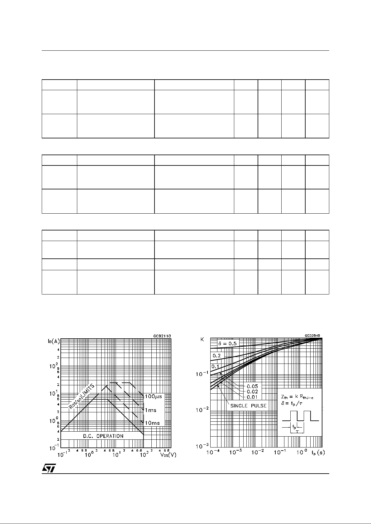
Saf e Oper ating A rea
Source-drain Current
(•)
Source-drain Current (pulsed)
(*)
Forward On Voltage
Reverse Recovery Time
Reverse Recovery Charge
Reverse Recovery Current
I
= 6 A VGS = 0
SD
= 6 A di/dt = 100A/µs
I
SD
V
= 10 V Tj = 150°C
DD
(see test circuit, Figure 5)
Thermal Impedance
6
24
1.3 V
70
175
5
ns
ns
ns
A
A
ns
nC
A
3/9
Page 4

STD6NF10
Output Characteristics Transfer Characteristics
Transconductance Static Drain-source On Resistance
Gate Charge vs Gate-source Voltage Capacitance Variations
4/9
Page 5

STD6NF10
Normalized Gate Threshold Voltage vs Temperature Normalized on Resistance vs Temperature
Source-drain Diode Forward Characteristics .
. .
5/9
Page 6

STD6NF10
Fig. 1: Unclamped Inductive Load Test CircuitFig. 1: Unclamped Inductive Load Test Circuit Fig. 2: Unclamped Inductive Waveform
Fig. 3: Switching Times Test Circuits For Resistive
Load
Fig. 5: Test Circuit For Inductive Load Switching
And Diode Recovery Times
Fig. 4: Gate Charge test Circuit
6/9
Page 7

STD6NF10
TO-251 (IPAK) MECHANI CAL DAT A
DIM.
mm inch
MIN. TYP. MAX. MIN. TYP. MAX.
A 2.2 2.4 0.086 0.094
A1 0.9 1.1 0.035 0.043
A3 0.7 1.3 0.027 0.051
B 0.64 0.9 0.025 0.031
B2 5.2 5.4 0.204 0.212
B3 0.85 0.033
B5 0.3 0.012
B6 0.95 0.037
C 0.45 0.6 0.017 0.023
C2 0.48 0.6 0.019 0.023
D 6 6.2 0.236 0.244
E 6.4 6.6 0.252 0.260
G 4.4 4.6 0.173 0.181
H 15.9 16.3 0.626 0.641
L 9 9.4 0.354 0.370
L1 0.8 1.2 0.031 0.047
L2 0.8 1 0.031 0.039
A
C2
L2
E
B2
= =
= =
H
C
A3
A1
B6
L
B
B5
G
= =
D
B3
2
1 3
L1
0068771-E
7/9
Page 8

STD6NF10
TO-252 (DPAK) MECHANICAL DATA
DIM.
mm inch
MIN. TYP. MAX. MIN. TYP. MAX.
A 2.2 2.4 0.086 0.094
A1 0.9 1.1 0.035 0.043
A2 0.03 0.23 0.001 0.009
B 0.64 0.9 0.025 0.035
B2 5.2 5.4 0.204 0.212
C 0.45 0.6 0.017 0.023
C2 0.48 0.6 0.019 0.023
D 6 6.2 0.236 0.244
E 6.4 6.6 0.252 0.260
G 4.4 4.6 0.173 0.181
H 9.35 10.1 0.368 0.397
L2 0.8 0.031
L4 0.6 1 0.023 0.039
A
C2
L2
E
B2
==
H
DETAIL "A"
D
==
C
B
2
1 3
L4
A1
G
==
A2
DETAIL "A"
0068772-B
8/9
Page 9

STD6NF10
Information furnished is believed to be accurate an d rel i able. However, STMicroelectro ni cs assumes no responsibility for the consequen ces
of use of such information nor for any infringement of patents or other rights of third parties which may result from its use. No license is granted
by implic ation or otherwise under any patent or patent ri ghts of STM i croelectr onics. Sp ecifications mentioned in thi s publication are subject
to change without notice. This publication supersedes and replaces all information previously supplied. STMicroelectronics product s are not
authorized for use as cri tical comp onents in lif e support devi ces or systems without express written approv al of STMicroel ectronics.
The ST log o i s registered trademark of STMicroelectronics
2001 STMi croelectronics - All Ri ghts Rese rved
All other names are the property of their respective ow ners.
Australi a - Brazil - China - Finland - France - G ermany - Ho ng K ong - India - It al y - Japan - Ma la ys i a - Malta - Mo rocco -
Singapor e - Spain - Sweden - Switze rl and - United Kingdom - U .S .A.
STMicroelect ro n ics GRO UP OF COMPANI ES
http://www.st.com
9/9
 Loading...