

Page 1
HIGH VOLTAGE NPN POWER TRANSISTOR
■ REVERSEPINS OUT Vs STANDARDIPAK
(TO-251)PACKAGE
■ HIGH VOLTAGECAPABILITY
■ HIGH DCCURRENT GAIN
■ THROUGH-HOLE IPAK(TO-251) POWER
PACKAGEIN TUBE
■ MINIMUMLOT-TO-LOTSPREAD FOR
RELIABLEOPERATION
APPLICATIONS:
■ SWITCHMODE POWERSUPPLIES
DESCRIPTION
The STD616A-1 is manufactured using High
Voltage Multi Epitaxial Planar technology for high
switching speeds and high voltage withstand
capability.
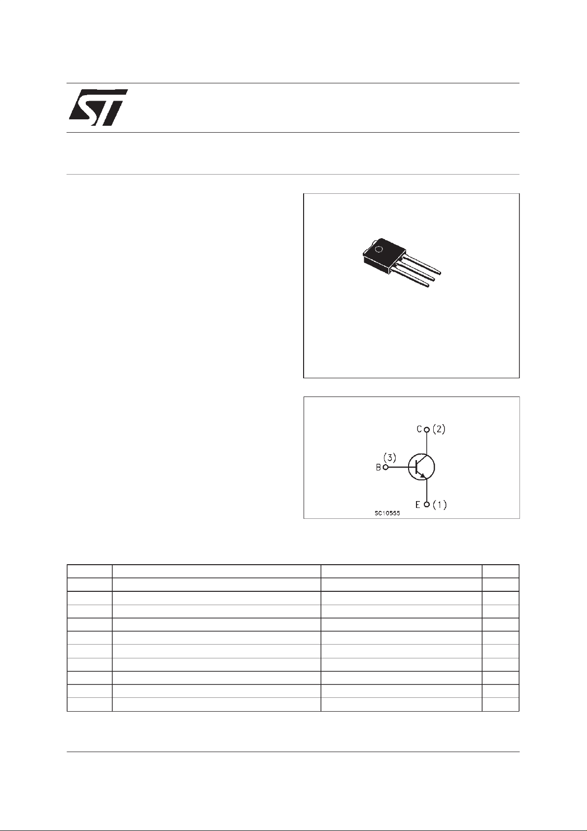
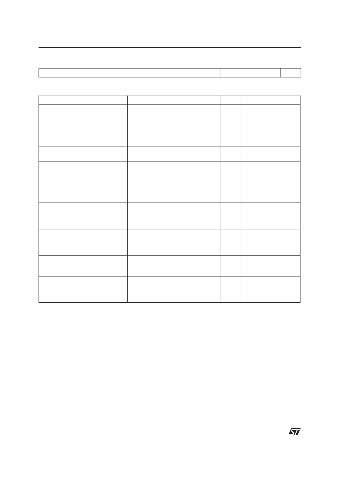
STD616A-1
3
2
1
IPAK
TO-251
INTERNAL SCHEMATIC DIAGRAM
ABSOLUTE MAXIMUM RATINGS
Symbol Parameter Value Unit
V
V
V
I
I
P
T
Collect or-E mitter Voltage (VBE=0) 1000 V
CES
Collect or-E mitter Voltage (IB= 0) 450 V
CEO
Emitter-Base Voltage (IC=0) 12 V
EBO
Collect or Current 1.6 A
I
C
Collect or Pe ak Current (tp<5ms) 2.4 A
CM
Base C urr ent 0.8 A
I
B
Base Peak Curre nt (tp<5ms) 1.2 A
BM
Tot al Di ss ipa t ion at Tc=25oC20W
tot
Storage Temperature -65 to 150
stg
Max. Operating Junc t io n Tem pe r ature 150
T
j
o
C
o
C
April 1999
1/5
Page 2
STD616A-1
THERMAL DATA
R
thj-case
Ther mal Resistance Junction- case Max 6.25
o
C/W
ELECTRICAL CHARACTERISTICS (T
=25oC unless otherwisespecified)
case
Symbol Parameter Test C ondition s Min. Typ. Max. Unit
I
CES
V
CEO(sus)
Collec t or Cut-off
Current (V
BE
=0V)
Collec t or -Emitter
V
= 1000 V
CE
= 1000 V Tj=125oC
V
CE
50
0.5
IC= 100 mA L = 25 mH 450 V
Sust aining Voltage
V
BEO
Collec t or -Base
IC=1mA 12 V
Sust aining Voltage
∗ Collec t or -Emitter
V
CE(sat)
Saturation Voltage
V
∗ Base-Emi tter
BE(sat)
Saturation Voltage
h
∗ DC Current Ga in
FE
RESI STIVE LO AD
t
t
on
s
t
f
Turn O n Time
Storage Time
Fall Time
RESI STIVE LO AD
t
t
on
s
t
f
Turn O n Time
Storage Time
Fall Time
INDUCTI V E LOAD
t
s
t
f
Storage Time
Fall Time
INDUCTI V E LOAD
t
s
t
f
Turn O n Time
Storage Time
IC=250mA IB=65mA
=0.8A IB=250mA
I
C
IC=250mA IB=65mA
=0.8A IB=250mA
I
C
=200µAVCE=5V
I
C
=300mA VCE=5V
I
C
I
=480mA VCE=5V
C
=1.6A VCE=5V
I
C
17
25
12
4
VCC= 250 V IC=250mA
=65mA IB2=-130mA 0.2
I
B1
VCC= 250 V IC=0.8A
=160mA IB2=-0.4A 1
I
B1
Vcl=300V IC=250mA
=65mA IB2=-130mA
I
B1
L=200µH
Vcl=300V IC= 0.8 A
I
=160mA IB2=-0.4A
B1
L=200µH
0.3
0.5
1.0
1.2
5
0.65
2.5
0.35
5
0.5
2.5
0.25
Fall Time
∗
Pulsed: Pulse duration = 300µs, duty cycle 1.5 %
µA
mA
V
V
V
V
µs
µs
µs
µs
µs
µs
µs
µs
µs
µs
2/5
Page 3

STD616A-1
Safe OperatingArea
ReverseBiased SOA
DeratingCurve
3/5
Page 4

STD616A-1
TO-251 (IPAK) MECHANICAL DATA
DIM.
A 2.20 2.40 0.087 0.094
A1 0.90 1.10 0.035 0.043
A3 0.70 1.30 0.028 0.051
B 0.64 0.90 0.025 0.035
B2 5.20 5.40 0.204 0.213
B3 0.85 0.033
B5 0.30 0.012
B6 0.95 0.037
C 0.45 0.60 0.018 0.024
C2 0.48 0.60 0.019 0.024
D 6.00 6.20 0.237 0.244
E 6.40 6.60 0.252 0.260
G 4.40 4.60 0.173 0.181
H 15.90 16.30 0.626 0.642
L 9.00 9.40 0.354 0.370
L1 0.80 1.20 0.031 0.047
L2 0.80 1.00 0.031 0.039
V1 10
MIN. TYP. MAX. MIN. TYP. MAX.
mm inch
o
10
o
4/5
P032N_E
Page 5

STD616A-1
Information furnished is believed to be accurate and reliable. However, STMicroelectronics assumes noresponsibility for theconsequences
of use of such information nor for any infringement of patents or other rights of third parties which may result from its use. No license is
granted by implication or otherwise under any patent or patent rights of STMicroelectronics. Specification mentioned in this publication are
subject tochange without notice.This publication supersedes and replaces all information previously supplied. STMicroelectronics products
are notauthorized for use as critical components in life support devices or systems without express written approval of STMicroelectronics.
The ST logo is a trademark of STMicroelectronics
1999 STMicroelectronics – Printedin Italy – AllRights Reserved
STMicroelectronicsGROUP OF COMPANIES
Australia -Brazil -Canada - China - France - Germany - Italy - Japan - Korea - Malaysia - Malta - Mexico - Morocco - The Netherlands -
Singapore -Spain - Sweden - Switzerland - Taiwan -Thailand - United Kingdom - U.S.A.
http://www.st.com
.
5/5
 Loading...