

Datasheet STP5NK40ZFP, STD5NK40ZT4, STD5NK40Z-1, STD5NK40Z Datasheet (SGS Thomson Microelectronics)
Page 1
1/13February 2003
STP5NK40Z - STP5NK40ZFP
STD5NK40Z - STD5NK40Z-1
N-CHANNEL 400V - 1.47Ω - 3A TO-220/TO-220FP/DPAK/IPAK
Zener-Protected SuperMESH™Power MOSFET
■ TYPICAL R
DS
(on) = 1.47 Ω
■ EXTREMELY HIGH dv/dt CAPABILITY
■ 100% AVALANCHE TESTED
■ GAT E CHARGE MINIMIZED
■ VERY LOW INTRINSIC CAPACITANCES
■ VER Y GO OD MANUFACTURING
REPEATIBILITY
DESCRIPTION
The SuperME SH™ series is obtained through an
extreme optimization of S T’s well established stripbased PowerMESH™ layout. In addition to pushing
on-resistance significantly down, special careis taken to ensure a very good dv/dt capability for the
most demanding applications. Such series com plements ST full range of high voltage MOSFETs including revolutionary MDm es h™ products.
APPLICATIONS
■ HIGH CURRENT, HIGH SPEED SWITCHING
■ IDEAL FOR OFF-LINE POWER SUPPLIES,
ADAPTORS AND PFC
■ LI GHTING
ORDERING INFORMATION
TYPE V
DSS
R
DS(on)
I
D
Pw
STP5NK40Z
STP5NK40ZFP
STD5NK40Z
STD5NK40Z-1
400 V
400 V
400 V
400 V
< 1.8 Ω
< 1.8 Ω
< 1.8 Ω
< 1.8 Ω
3A
3A
3A
3A
45 W
20 W
45 W
45 W
SALES TYPE MARKING PACKAGE PACKAGING
STP5NK40Z P5NK40Z TO-220 TUBE
STP5NK40ZFP P5NK40ZFP TO-220FP TUBE
STD5NK40ZT4 D5NK40Z DPAK TAPE & REEL
STD5NK40Z-1 D5NK40Z IPAK TUBE
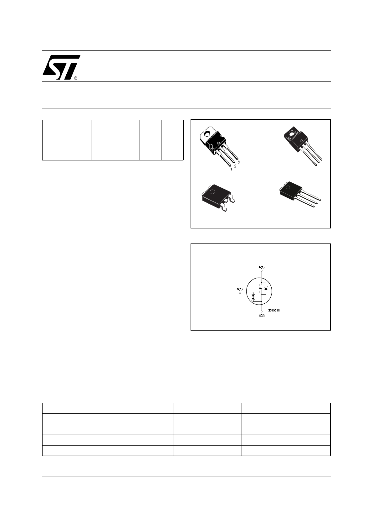
TO-220 TO-220FP
1
2
3
1
3
DPAK
3
2
1
IPAK
INTERNAL SCHEMATIC DIAGRAM
Page 2
STP5NK40Z - STP5NK40ZFP - STD5NK40Z - STD5NK40Z -1
2/13
ABSOLUTE MAXIMUM RATINGS
() Pulse width limited by safe operating area
(1) I
SD
≤3A, di/dt ≤200A/µs, VDD≤ V
(BR)DSS,Tj≤TJMAX.
(*) Limited only by maximum temperature allowed
THERMAL DATA
AVALANCHE CHARACTERISTICS
GATE-SOURCE ZENER DIODE
PROTECTION FEATURES OF GATE-TO-SOURCE ZENER DIODES
The built-in back-to-back Zener diodes have specifically been designed t o enhance not only the device’s
ESD capability, but also to make them safely absorb possible voltage transients that may occasionally be
applied from gate to source. In this respect the Zener voltage is appropriate to achieve an efficient and
cost-effective intervention to protect the device’ s integrity. These integ rated Zener diodes thus avoid the
usage of external components.
Symbol Parameter Value Unit
STP5NK40Z STP5NK40ZFP
STD5NK40Z
STD5NK40Z-1
V
DS
Drain-source Voltage (VGS=0)
400 V
V
DGR
Drain-gate Voltage (RGS=20kΩ)
400 V
V
GS
Gate- source Voltage ± 30 V
I
D
Drain Current (continuous) at TC= 25°C
3 3 (*) 3 A
I
D
Drain Current (continuous) at TC= 100°C
1.9 1.9 (*) 1.9 A
I
DM
()
Drain Current (pulsed) 12 12 (*) 12 A
P
TOT
Total Dissipation at TC= 25°C
45 20 45 W
Derating Factor 0.36 0.16 0.36 W/°C
V
ESD(G-S)
Gate source ESD(HBM-C=100pF, R=1.5KΩ) 2800 V
dv/dt (1) Peak Diode Recovery voltage slope 4.5 V/ns
V
ISO
Insulation Withstand Voltage (DC) - 2500 - V
T
j
T
stg
Operating Junction Temperature
Storage Temperature
-55to150
-55to150
°C
°C
TO-220 TO-220FP DPAK
Rthj-case Thermal Resistance Junction-case Max 2.77 6.25 2.77 °C/W
Rthj-amb Thermal Resistance Junction-ambient Max 62.5 100 °C/W
T
l
Maximum Lead Temperature For Soldering Purpose
300 °C
Symbol Parameter Max Value Unit
I
AR
Avalanche Current, Repetitive or Not-Repetitive
(pulse width limited by T
j
max)
3A
E
AS
Single Pulse Avalanche Energy
(starting T
j
= 25 °C, ID=IAR,VDD=50V)
130 mJ
Symbol Parameter Test Conditions Min. Typ. Max. Unit
BV
GSO
Gate-Source Breakdown
Voltage
Igs=± 1mA (Open Drain) 30 V
Page 3
3/13
STP5NK40Z - STP5NK 40Z FP - STD5NK40Z - STD5NK40Z-1
ELECTRICAL CHARACTERISTICS (T
CASE
=25°C UNLESS OTHERWISE SP ECIFIED)
ON/OFF
DYNAMIC
SWITCHING ON
SWITCHING OFF
SOURCE DRAIN DIODE
Note: 1. Pulsed: Pulse duration = 300 µs, duty cycle 1.5 %.
2. Pulse width limited by safe operating area.
3. C
oss eq.
is defined as a constant equivalent capacitance giving the same charging time as C
oss
when VDSincreases from 0 to 80%
V
DSS
.
Symbol Parameter Test Conditions Min. Typ. Max. Unit
V
(BR)DSS
Drain-source
Breakdown Voltage
ID=1 mA, VGS= 0 400 V
I
DSS
Zero Gate Voltage
Drain Current (V
GS
=0)
V
DS
= Max Rating
VDS= Max Rating, TC= 125 °C
1
50
µA
µA
I
GSS
Gate-body Leakage
Current (V
DS
=0)
V
GS
= ± 20V ±10 µA
V
GS(th)
Gate Threshold Voltage
V
DS=VGS,ID
= 50µA
3 3.75 4.5 V
R
DS(on)
Static Drain-source On
Resistance
VGS=10V,ID= 1.5 A 1.47 1.8 Ω
Symbol Parameter Test Conditions Min. Typ. Max. Unit
g
fs
(1) Forward Transconductance VDS=15 V,ID= 1.5 A 2.2 S
C
iss
C
oss
C
rss
Input Capacitance
Output Capacitance
Reverse Transfer
Capacitance
V
DS
=25V,f=1MHz,VGS= 0 305
57
11.5
pF
pF
pF
C
oss eq.
(3) Equivalent Output
Capacitance
VGS=0V,VDS= 0V to 400V 44 pF
Symbol Parameter Test Conditions Min. Typ. Max. Unit
t
d(on)
t
r
Turn-on Delay Time
Rise Time
VDD=200V,ID= 1.5 A
RG= 4.7Ω VGS=10V
(Resistive Load see, Figure 3)
9.2
6
ns
ns
Q
g
Q
gs
Q
gd
Total Gate Charge
Gate-Source Charge
Gate-Drain Charge
V
DD
=320V,ID=3A,
V
GS
=10V
11.7
2.8
5.8
17 nC
nC
nC
Symbol Parameter Test Conditions Min. Typ. Max. Unit
t
d(off)
t
f
Turn-off Delay Time
Fall Time
VDD= 200 V, ID= 1.5A
R
G
=4.7ΩVGS=10V
(Resistive Load see, Figure 3)
22.5
11
ns
ns
t
r(Voff)
t
f
t
c
Off-voltage Rise Time
Fall Time
Cross-over Time
V
DD
= 320V, ID=3A,
RG=4.7Ω, VGS= 10V
(Inductive Load see, Figure 5)
8.5
7.5
14.5
ns
ns
ns
Symbol Parameter Test Conditions Min. Typ. Max. Unit
I
SD
I
SDM
(2)
Source-drain Current
Source-drain Current (pulsed)
3
12
A
A
VSD(1)
Forward On Voltage
ISD= 3 A, VGS=0
1.6 V
t
rr
Q
rr
I
RRM
Reverse Recovery Time
Reverse Recovery Charge
Reverse Recovery Current
I
SD
= 3 A, di/dt = 100A/µs
VDD=40V,Tj= 150°C
(see test circuit, Figure 5)
145
464
6.4
ns
nC
A
Page 4
STP5NK40Z - STP5NK40ZFP - STD5NK40Z - STD5NK40Z -1
4/13
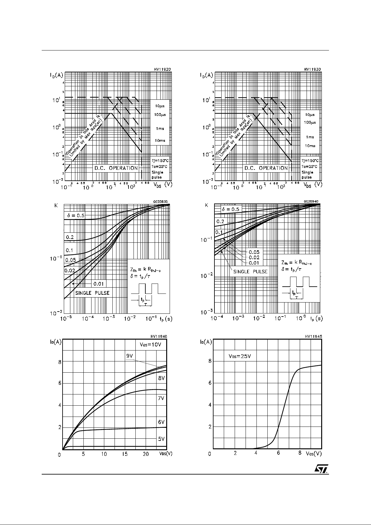
Thermal Impedan ce For TO-220/DPAK/IPAK
Output Characteristics
Safe Operating Area For TO-220FPSafe Operating Area For TO-220/DPAK/IPAK
Thermal Impedance For TO-220F P
Transfer Characteristics
Page 5

5/13
STP5NK40Z - STP5NK 40Z FP - STD5NK40Z - STD5NK40Z-1
Normalized Gate Threshold Voltage vs Temp. Normalized On Resistance vs Temperature
Capacitance VariationsGate Charge vs Gate-so urce Voltage
Static Drain-source On ResistanceTransconductance
Page 6

STP5NK40Z - STP5NK40ZFP - STD5NK40Z - STD5NK40Z -1
6/13
Source-drain Diode Forward Characteristics Normalized BVDSS vs Temperature
Maximum Avalanche Energy vs Temperature
Page 7

7/13
STP5NK40Z - STP5NK 40Z FP - STD5NK40Z - STD5NK40Z-1
Fig. 5: Test Circuit For Induct ive Load Switching
And Diode Recovery T imes
Fig. 4: Gate Charge test Circuit
Fig. 2: Unclamped Inductive WaveformFig. 1: Unclamped Inductive Load Test Circuit
Fig. 3: Switching Times Test Circuit For
Resistive Load
Page 8

STP5NK40Z - STP5NK40ZFP - STD5NK40Z - STD5NK40Z -1
8/13
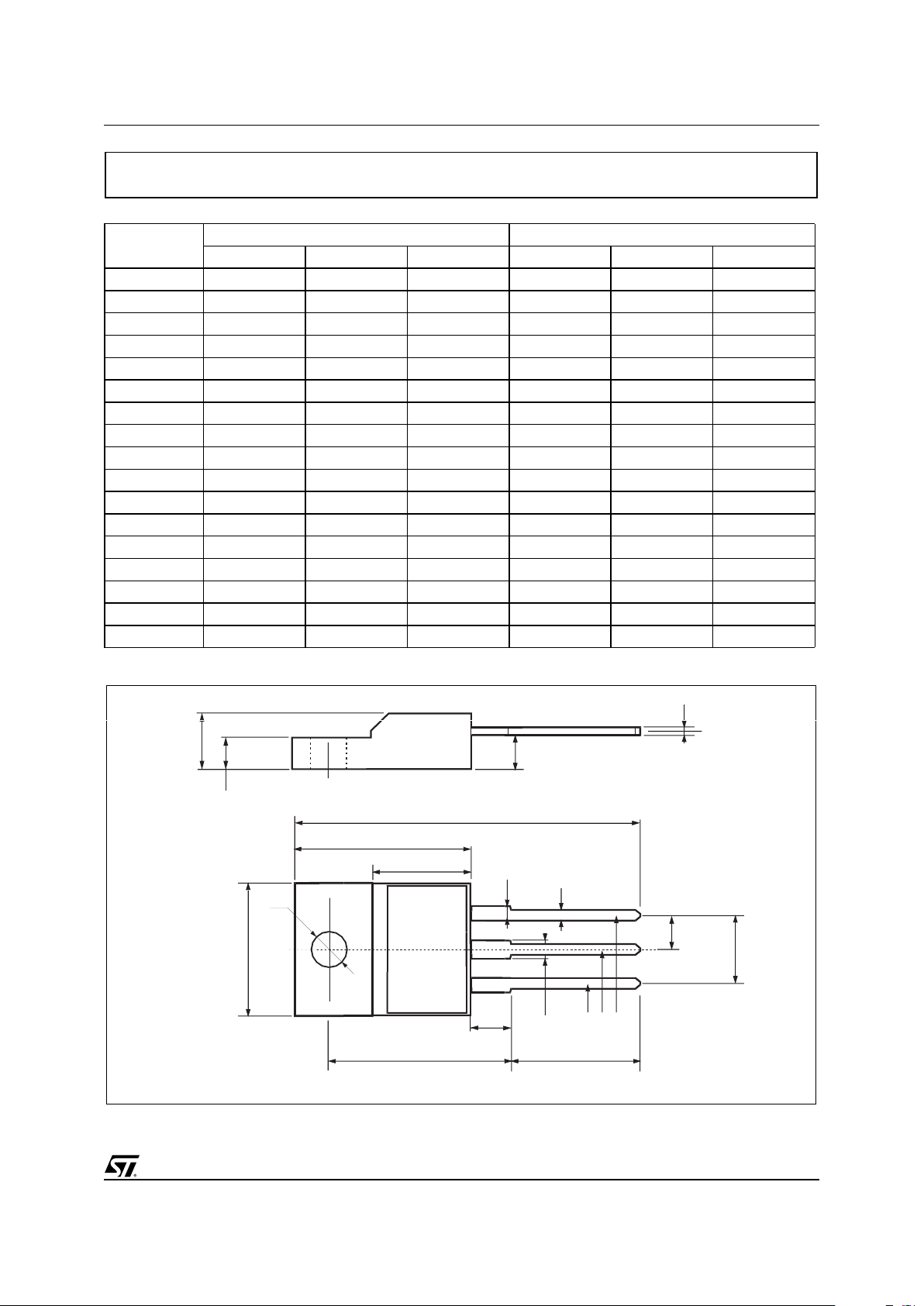
DIM.
mm inch
MIN. TYP. MAX. MIN. TYP. MAX.
A 4.40 4.60 0.173 0.181
C 1.23 1.32 0.048 0.051
D 2.40 2.72 0.094 0.107
D1 1.27 0.050
E 0.49 0.70 0.019 0.027
F 0.61 0.88 0.024 0.034
F1 1.14 1.70 0.044 0.067
F2 1.14 1.70 0.044 0.067
G 4.95 5.15 0.194 0.203
G1 2.4 2.7 0.094 0.106
H2 10.0 10.40 0.393 0.409
L2 16.4 0.645
L4 13.0 14.0 0.511 0.551
L5 2.65 2.95 0.104 0.116
L6 15.25 15.75 0.600 0.620
L7 6.2 6.6 0.244 0.260
L9 3.5 3.93 0.137 0.154
DIA. 3.75 3.85 0.147 0.151
L6
A
C
D
E
D1
F
G
L7
L2
Dia.
F1
L5
L4
H2
L9
F2
G1
TO-220 MECHANICAL DATA
P011C
Page 9
9/13
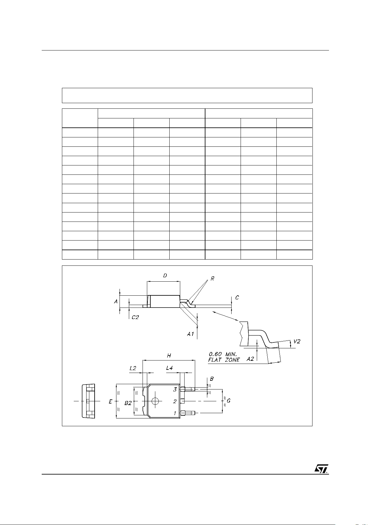
STP5NK40Z - STP5NK 40Z FP - STD5NK40Z - STD5NK40Z-1
L2
A
B
D
E
H
G
L6
¯
F
L3
G1
123
F2
F1
L7
L4
L5
DIM.
mm. inch
MIN. TYP MAX. MIN. TYP. MAX.
A 4.4 4.6 0.173 0.181
B 2.5 2.7 0.098 0.106
D 2.5 2.75 0.098 0.108
E 0.45 0.7 0.017 0.027
F 0.75 1 0.030 0.039
F1 1.15 1.5 0.045 0.067
F2 1.15 1.5 0.045 0.067
G 4.95 5.2 0.195 0.204
G1 2.4 2.7 0.094 0.106
H 10 10.4 0.393 0.409
L2 16 0.630
L3 28.6 30.6 1.126 1.204
L4 9.8 10.6 .0385 0.417
L5 2.9 3.6 0.114 0.141
L6 15.9 16.4 0.626 0.645
L7 9 9.3 0.354 0.366
Ø 3 3.2 0.118 0.126
TO-220FP MECHANICAL DATA
Page 10
STP5NK40Z - STP5NK40ZFP - STD5NK40Z - STD5NK40Z -1
10/13
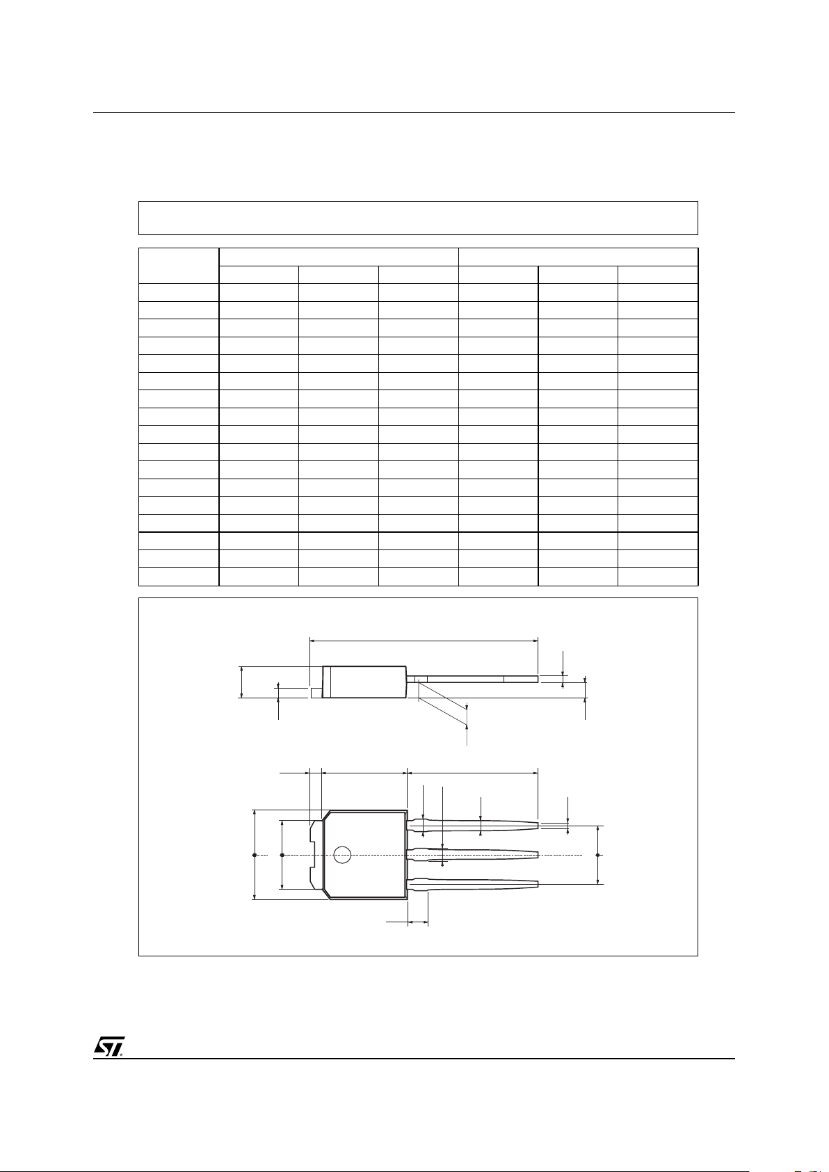
DIM.
mm inch
MIN. TYP. MAX. MIN. TYP. MAX.
A 2.20 2.40 0.087 0.094
A1 0.90 1.10 0.035 0.043
A2 0.03 0.23 0.001 0.009
B 0.64 0.90 0.025 0.035
B2 5.20 5.40 0.204 0.213
C 0.45 0.60 0.018 0.024
C2 0.48 0.60 0.019 0.024
D 6.00 6.20 0.236 0.244
E 6.40 6.60 0.252 0.260
G 4.40 4.60 0.173 0.181
H 9.35 10.10 0.368 0.398
L2 0.8 0.031
L4 0.60 1.00 0.024 0.039
V2 0
o
8
o
0
o
0
o
P032P_B
TO-252 (DPAK) MECHANICAL DATA
Page 11
11/13
STP5NK40Z - STP5NK 40Z FP - STD5NK40Z - STD5NK40Z-1
DIM.
mm inch
MIN. TYP. MAX. MIN. TYP. MAX.
A 2.2 2.4 0.086 0.094
A1 0.9 1.1 0.035 0.043
A3 0.7 1.3 0.027 0.051
B 0.64 0.9 0.025 0.031
B2 5.2 5.4 0.204 0.212
B3 0.85 0.033
B5 0.3 0.012
B6 0.95 0.037
C 0.45 0.6 0.017 0.023
C2 0.48 0.6 0.019 0.023
D 6 6.2 0.236 0.244
E 6.4 6.6 0.252 0.260
G 4.4 4.6 0.173 0.181
H 15.9 16.3 0.626 0.641
L 9 9.4 0.354 0.370
L1 0.8 1.2 0.031 0.047
L2 0.8 1 0.031 0.039
A
C2
C
A3
H
A1
D
L
L2
L1
1 3
= =
B3
B
B6
B2
E
G
= =
= =
B5
2
TO-251 (IPAK) MECHANICAL DATA
0068771-E
Page 12

STP5NK40Z - STP5NK40ZFP - STD5NK40Z - STD5NK40Z -1
12/13
TAPE AND REEL SHIPMENT (suffix ”T4”)*
TUBE SHIPMENT (no suffix)*
DPAK FOOTPRINT
* on sales ty pe
DIM.
mm inch
MIN. MAX. MIN. MAX.
A 330 12.992
B 1.5 0.059
C 12.8 13.2 0.504 0.520
D 20.2 0.795
G 16.4 18.4 0.645 0.724
N 50 1.968
T 22.4 0.881
BASE QTY BULK QTY
2500 2500
REEL MECHANICAL DATA
DIM.
mm inch
MIN. MAX. MIN. MAX.
A0 6.8 7 0.267 0.275
B0 10.4 10.6 0.409 0.417
B1 12.1 0.476
D 1.5 1.6 0.059 0.063
D1 1.5 0.059
E 1.65 1.85 0.065 0.073
F 7.4 7.6 0.291 0.299
K0 2.55 2.75 0.100 0.108
P0 3.9 4.1 0.153 0.161
P1 7.9 8.1 0.311 0.319
P2 1.9 2.1 0.075 0.082
R 40 1.574
W 15.7 16.3 0.618 0.641
TAPE MECHANICAL DATA
All dimensions
areinmillimeters
All dimensions are in millimeters
Page 13

13/13
STP5NK40Z - STP5NK 40Z FP - STD5NK40Z - STD5NK40Z-1
Information furnished is believed to be accurate and reliable. However, STMicroelectronics assumes no responsibility for the
consequences of u se of such inf ormat ion nor for any in fring ement of p aten ts or othe r ri ghts of th ird p arties whic h may resul t f rom
its use. No license is granted by implication or otherwise under any patent or patent rights of STMicroelectronics. Specifications
mentioned in this publication are subject to change without notice. This publication supersedes and replaces all information
previously supplied. STMicroelectronics products are not authorized for use as critical components in life support devices or
systems without express written approval of STMicroelectronics.
© The ST logo is a registered trademark of STMicroelectronics
© 2003 STMicroelectronics - Printed in Italy - All Rights Reserved
STMicroelectronics GROUP OF COMPANIES
Australia - Brazil - Canada - China - Finland - France - Germany - Hong Kong - India - Israel - Italy - Japan - Malaysia - Malta - Morocco
Singapore - Spain - Sweden - Switzerland - United Kingdom - United States.
© http://www.st.com
 Loading...