

Page 1
STD5NE10L
N - CHANNEL 100V - 0.3
TYPE V
ST D5 NE10L 100 V < 0.4 Ω 5A
■ TYPICALR
■ EXCEPTIONAL dv/dt CAPABILITY
■ AVALANCHERUGGEDTECHNOLOGY
■ 100 % AVALANCHE TESTED
■ APPLICATIONORIENTED
DS(on)
DSS
= 0.3 Ω
CHARACTERIZATION
■ FORTAPE & REELAND OTHER
PACKAGINGOPTIONSCONTACT SALES
OFFICES
DESCRIPTION
This Power MOSFET is the latest developmentof
STMicroelectronics unique ” Single Feature
Size” strip-based process. The resulting transistor shows extremely high packing density for
low on-resistance, rugged avalanche characteristicsand less criticalalignment steps therefore
a remarkablemanufacturingreproducibility.
R
DS(on)
I
D
Ω
- 5A - DPAK/IPAK
STripFET POWER MOSFET
PRELIMINARY DATA
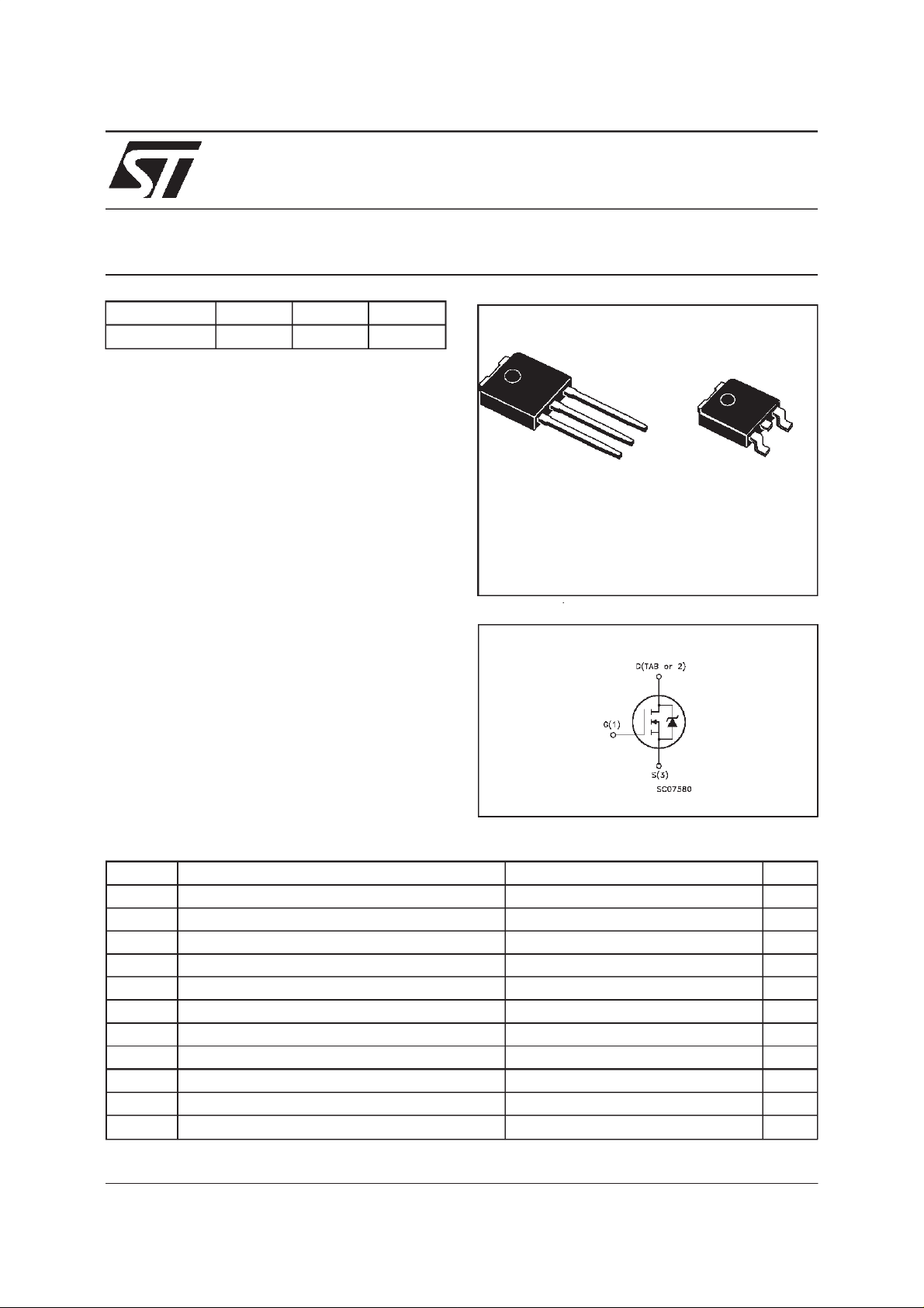
3
2
1
IPAK
TO-251
(Suffix ”-1”)
DPAK
TO-252
(Suffix ”T4”)
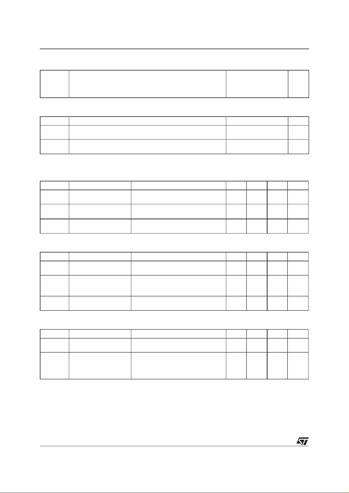
INTERNAL SCHEMATIC DIAGRAM
3
1
APPLICATIONS
■ DC MOTOR CONTROL (DISK DRIVES,etc.)
■ DC-DC& DC-AC CONVERTERS
■ SYNCHRONOUS RECTIFICATION
ABSOLUTE MAXIMUM RATINGS
Symbol Parameter Val u e Uni t
V
V
V
I
DM
P
dv/ dt (
T
(•) Pulse width limited by safe operating area (1)ISD≤ 5 A, di/dt ≤ 200 A/µs, VDD≤ V
October 1998
Drain-source Voltage (VGS=0) 100 V
DS
Drain- ga t e Volt age (RGS=20kΩ)
DGR
Gat e- source Vol tage ± 20 V
GS
I
Drain Current (continuous) at Tc=25oC5A
D
I
Drain Current (continuous) at Tc=100oC3.5A
D
(•) Dr ain Current (puls ed ) 20 A
Total Dissipation at Tc=25oC25W
tot
Derat i ng Fact or 0.2 W/
1) Peak Diode Recovery vol tage slope 6 V /ns
Sto rage Temper at u re -65 to 1 50
stg
T
Max. Ope r ating Junction Tempera t ur e 150
j
100 V
(BR)DSS,Tj≤TJMAX
o
C
o
C
o
C
1/5
Page 2
STD5NE10L
THERMAL DATA
R
thj-case
R
thj-amb
R
thc-sink
T
AVALANCHE CHARACTERISTICS
Symbol Para meter Max Val ue Uni t
I
AR
E
Ther mal Resistanc e Juncti on-case Max
Ther mal Resistanc e Juncti on-ambien t Max
Thermal Resistance Case-sink Typ
Maximum Lead Temperature F or S oldering Pu rpose
l
Avalanche Curr ent, Repetit ive or Not-Repetit ive
(pulse width limited by T
Single Pu lse Avalanche Energy
AS
(starting T
=25oC, ID=IAR,VDD=30V)
j
max)
j
5
100
1.5
275
5A
20 mJ
o
C/W
o
C/W
o
C/W
o
C
ELECTRICAL CHARACTERISTICS (T
=25oC unless otherwisespecified)
case
OFF
Symbol Parameter Test Condit ions Min. Typ. Max. Unit
V
(BR)DSS
Drain-source
=250µAVGS=0
I
D
100 V
Break d own Voltage
I
DSS
I
GSS
Zero Gate Voltage
Drain Current (V
GS
Gat e- b ody Le akage
Current (V
DS
=0)
=0)
V
=MaxRating
DS
= Max Rating Tc=100oC
V
DS
= ± 20 V
V
GS
1
10
± 100 nA
ON(∗)
Symbol Parameter Test Condit ions Min. Typ. Max. Unit
V
GS(th)
Gate Threshold
V
DS=VGSID
= 250 µA
11.72.5V
Voltage
R
DS(on)
I
D(on)
Static Drain-source On
Resistance
VGS=10V ID=2.5A
=5V ID=2.5A
V
GS
On State D ra in Cur rent VDS>I
D(on)xRDS(on )max
0.3
0.35
5A
0.4
0.45
VGS=10V
DYNAMIC
Symbol Parameter Test Condit ions Min. Typ. Max. Unit
g
(∗)Forward
fs
Tr ansconductance
C
C
C
Input Capacitan c e
iss
Out put Capacitanc e
oss
Reverse Transf er
rss
Capacitance
VDS>I
D(on)xRDS(on )maxID
=2.5 A 2 S
VDS=25V f=1MHz VGS=0 345
45
20
450
60
25
µA
µ
Ω
Ω
pF
pF
pF
A
2/5
Page 3

STD5NE10L
ELECTRICAL CHARACTERISTICS
(continued)
SWITCHING ON
Symbol Parameter Test Condit ions Min. Typ. Max. Unit
t
d(on)
Q
Q
Q
Turn-on Time
t
Rise Time
r
Total Gate Charge
g
Gat e- Source Char ge
gs
Gate-Drain Charge
gd
VDD=50V ID=2.5A
=4.7 Ω VGS=5V
R
G
7
17
VDD=80V ID=5A VGS=5V 10
5
4
9
22
14 nC
SWITCHING OFF
Symbol Parameter Test Condit ions Min. Typ. Max. Unit
t
r(Voff)
t
t
Off -voltage Rise Time
Fall Time
f
Cross-over T i m e
c
VDD=80V ID=5A
=4.7 Ω VGS=10V
R
G
8
9
19
10
12
25
SOURCEDRAINDIODE
Symbol Parameter Test Condit ions Min. Typ. Max. Unit
I
SD
I
SDM
V
SD
t
Q
I
RRM
(∗) Pulsed: Pulse duration = 300 µs, duty cycle 1.5%
(•) Pulse width limited by safe operating area
Source-drain Curr ent
(•)
Source-drain Curr ent
5
20
(pulsed)
(∗) Forwar d On V oltage ISD=8A VGS=0 1.5 V
Reverse Recov ery
rr
Time
Reverse Recov ery
rr
=5A di/dt=100A/µs
I
SD
=30V Tj=150oC
V
DD
75
190
Charge
Reverse Recov ery
5
Current
ns
ns
nC
nC
ns
ns
ns
A
A
ns
µ
A
C
3/5
Page 4

STD5NE10L
TO-252 (DPAK) MECHANICAL DATA
DIM.
mm inch
MIN. TYP. MAX. MIN. TYP. MAX.
A 2.2 2.4 0.086 0.094
A1 0.9 1.1 0.035 0.043
A2 0.03 0.23 0.001 0.009
B 0.64 0.9 0.025 0.035
B2 5.2 5.4 0.204 0.212
C 0.45 0.6 0.017 0.023
C2 0.48 0.6 0.019 0.023
D 6 6.2 0.236 0.244
E 6.4 6.6 0.252 0.260
G 4.4 4.6 0.173 0.181
H 9.35 10.1 0.368 0.397
L2 0.8 0.031
L4 0.6 1 0.023 0.039
4/5
H
A
E
C2
L2
B2
==
==
DETAIL”A”
D
2
13
L4
A1
C
A2
DETAIL”A”
B
G
==
0068772-B
Page 5

TO-251(IPAK) MECHANICAL DATA
STD5NE10L
DIM.
MIN. TYP. MAX. MIN. TYP. MAX.
mm inch
A 2.2 2.4 0.086 0.094
A1 0.9 1.1 0.035 0.043
A3 0.7 1.3 0.027 0.051
B 0.64 0.9 0.025 0.031
B2 5.2 5.4 0.204 0.212
B3 0.85 0.033
B5 0.3 0.012
B6 0.95 0.037
C 0.45 0.6 0.017 0.023
C2 0.48 0.6 0.019 0.023
D 6 6.2 0.236 0.244
E 6.4 6.6 0.252 0.260
G 4.4 4.6 0.173 0.181
H 15.9 16.3 0.626 0.641
L 9 9.4 0.354 0.370
L1 0.8 1.2 0.031 0.047
L2 0.8 1 0.031 0.039
H
A
E
==
C2
L2
B2
==
D
B3
2
13
L1
B6
A1
C
A3
L
B
B5
G
==
0068771-E
5/5
Page 6

STD5NE10L
Information furnished is believed to be accurate and reliable. However, STMicroelectronics assumes no responsibility forthe consequences
of use of such information nor for any infringement of patents or other rights of third parties which may result from its use. No license is
granted by implicationor otherwise under any patent or patent rights of STMicroelectronics. Specification mentioned in thispublication are
subject to change without notice. This publication supersedes and replaces all information previously supplied. STMicroelectronics products
are not authorized for use as critical components inlife support devices or systems withoutexpress written approval of STMicroelectronics.
The ST logo is a registered trademark of STMicroelectronics
1998 STMicroelectronics – Printed in Italy – All Rights Reserved
STMicroelectronics GROUP OF COMPANIES
Australia - Brazil - Canada -China -France - Germany - Italy - Japan - Korea -Malaysia - Malta - Mexico - Morocco - The Netherlands -
Singapore - Spain - Sweden - Switzerland - Taiwan - Thailand - United Kingdom - U.S.A.
http://www.st.com
.
6/5
 Loading...