

Page 1
STD5NB30
N - CHANNEL300V - 0.75
TYPE V
DSS
ST D5N B3 0 300 V < 0.9 Ω 5A
■ TYPICALR
■ EXTREMELYHIGH dv/dt CAPABILITY
■ 100%AVALANCHETESTED
■ VERYLOW INTRINSIC CAPACITANCES
■ GATECHARGE MINIMIZED
■ ADDSUFFIX ”T4” FORORDERING IN TAPE
DS(on)
= 0.75 Ω
& REEL
DESCRIPTION
Using the latest high voltage MESH OVERLAY
process, STMicroelectronics has designed an
advanced family of power MOSFETs with
outstanding performances. The new patent
pending strip layout coupled with the Company’s
proprietary edge termination structure, gives the
lowest R
per area, exceptional avalanche
DS(on)
and dv/dt capabilities and unrivalled gate charge
and switching characteristics.
R
DS(on)
I
D
Ω
- 5A - DPAK
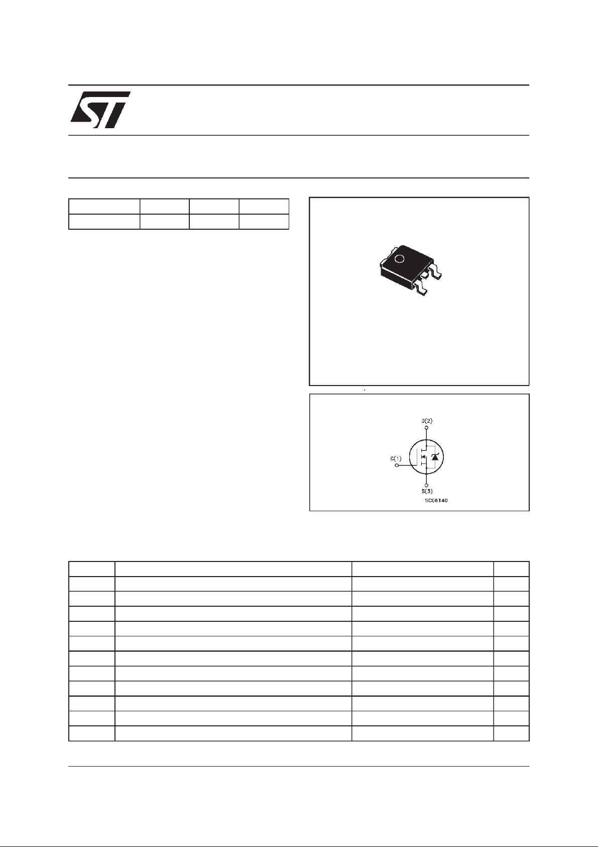
PowerMESH MOSFET
3
1
DPAK
TO-252
(Suffix ”T4”)
INTERNAL SCHEMATIC DIAGRAM
APPLICATIONS
■ SWITCHMODE POWER SUPPLIES (SMPS)
■ DC-AC CONVERTERS FOR WELDING
EQUIPMENTANDUNINTERRUPTIBLE
POWERSUPPLIESAND MOTORDRIVE
ABSOLUTE MAXIMUM RATINGS
Symbol Parameter Value Unit
V
V
V
I
DM
P
dv/dt(
T
(•) Pulse width limited by safeoperating area (1)ISD≤ 5Α,
August 1999
Dra in- sour c e Vol t age (VGS= 0) 300 V
DS
Dra in- gate Volt age (RGS=20kΩ)
DGR
Gat e-source Voltage ± 30 V
GS
I
Dra in Current (c ont in uous ) at Tc=25oC5A
D
I
Dra in Current (c ont in uous ) at Tc=100oC3A
D
300 V
(•) Dra in Current (p ulsed ) 20 A
Tot al Dissipation at Tc=25oC55W
tot
Der ati ng Factor 0.44 W/
1) Peak Diode Recover y v olt age slope 5.5 V/ns
St orage Temperatur e -65 t o 150
stg
T
Max. O perating J unction T emperat ure 150
j
δι/δτ ≤ 200 A/µs, VDD≤ V
(BR)DSS
,Tj≤T
JMAX
o
C
o
C
o
C
1/9
Page 2
STD5NB30
THERMAL DATA
R
thj-case
Rthj-a mb
R
thc-sink
T
AVALANCHE CHARACTERISTICS
Symbol Parameter Max Value Unit
I
AR
E
Ther mal Resistanc e Junct ion-case Max
Ther mal Resistanc e Junct ion-ambient Max
Ther mal Resistanc e Case-sink Ty p
Maximum Lead Te m pe ra t ure For S o lder ing Purp os e
l
Avalanche Current, Repetitive or Not-Repetitive
(pulse width limited by T
Single P ul s e Avalan c he Energy
AS
(starting T
=25oC, ID=IAR,VDD=50V)
j
max)
j
2.27
100
1.5
275
5A
40 mJ
o
C/W
oC/W
o
C/W
o
C
ELECTRICAL CHARACTERISTICS (T
=25oC unless otherwisespecified)
case
OFF
Symbol Parameter Test Conditions Min. Typ. Max. Unit
V
(BR)DSS
Drain-source
=250µAVGS=0
I
D
300 V
Break dow n Volt age
I
DSS
I
GSS
Zero Gate Voltage
Drain Cur rent (V
GS
Gat e- bod y L eak ag e
Current (V
DS
=0)
=0)
V
=MaxRating
DS
=MaxRating Tc=125oC
V
DS
= ± 30 V
V
GS
1
50
± 100 nA
ON(∗)
Symbol Parameter Test Conditions Min. Typ. Max. Unit
V
GS(th)
R
DS(on)
Gate Threshold Voltage
Sta t ic Drain -s ource On
V
DS=VGSID
= 250 µ A
VGS=10V ID=2.5 A 0.75 0.9
345V
Resistance
I
D(on)
On State Drain Current VDS>I
D(on)xRDS(on)max
5A
VGS=10V
DYNAMIC
Symbol Parameter Test Conditions Min. Typ. Max. Unit
g
(∗)Forward
fs
Tr ansc on duc tance
C
C
C
Input Capac i t ance
iss
Out put Capacitanc e
oss
Reverse Tr ansfer
rss
Capacit a nc e
VDS>I
D(on)xRDS(on)maxID
=3A 2 3.3 S
VDS=25V f=1MHz VGS= 0 500
100
14
µA
µ
Ω
pF
pF
pF
A
2/9
Page 3
STD5NB30
ELECTRICAL CHARACTERISTICS (continued)
SWITCHINGON
Symbol Parameter Test Conditions Min. Typ. Max. Unit
t
d(on)
t
Turn-on delay Time
Rise Ti m e
r
VDD=150V ID=3A
=4.7 Ω VGS=10V
R
G
(see test circuit, figure 3)
Q
Q
Q
Tot al Gat e Charge
g
Gat e- Source Charge
gs
Gate-Drain Charge
gd
VDD= 250 V ID=5 A VGS=10V 17
SWITCHINGOFF
Symbol Parameter Test Conditions Min. Typ. Max. Unit
t
r(Voff)
t
Off-voltage Rise Tim e
t
Fall T ime
f
Cross-over T ime
c
VDD=240V ID=6 A
=4.7 Ω VGS=10V
R
G
(see test circuit, figure 5)
SOURCEDRAINDIODE
Symbol Parameter Test Conditions Min. Typ. Max. Unit
I
SD
I
SDM
V
SD
t
Q
I
RRM
(∗) Pulsed: Pulse duration = 300 µs, duty cycle 1.5 %
(•) Pulse width limited by safe operatingarea
Source-drain Current
(•)
Source-drain Current
(pulsed)
(∗)ForwardOnVoltage ISD=6A VGS=0 1.6 V
Reverse Recovery
rr
Time
Reverse Recovery
rr
=6A di/dt=100A/µs
I
SD
= 100 V Tj=150oC
V
DD
(see test circuit, figure 5)
Charge
Reverse Recovery
Current
13
8
25 nC
7.5
6.5
8
15
7
5
20
190
1.1
11.5
ns
ns
nC
nC
ns
ns
ns
A
A
ns
µ
A
C
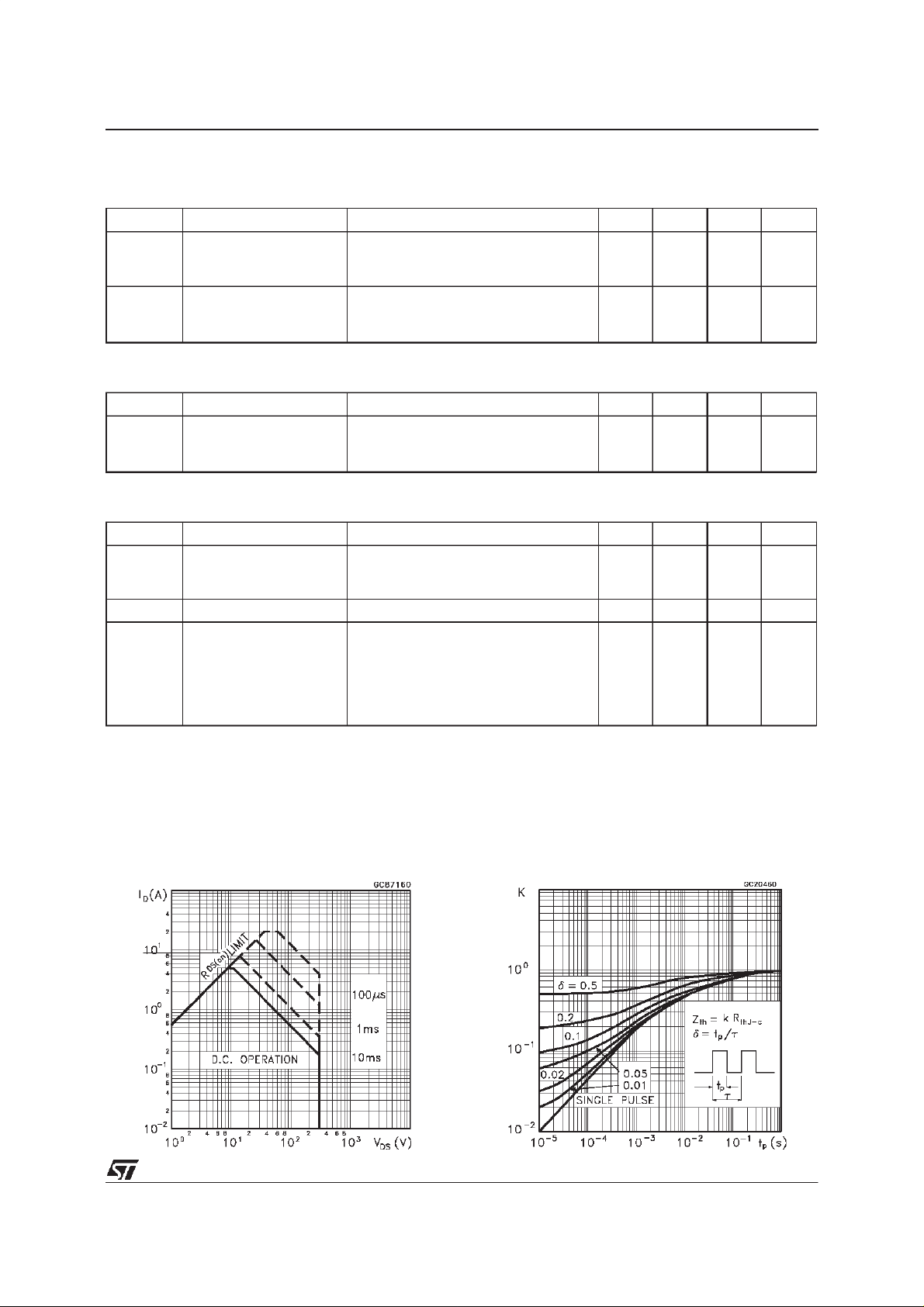
SafeOperating Area ThermalImpedance
3/9
Page 4

STD5NB30
OutputCharacteristics
Transconductance
TransferCharacteristics
Static Drain-sourceOn Resistance
Gate Charge vs Gate-sourceVoltage
4/9
CapacitanceVariations
Page 5

STD5NB30
NormalizedGate Threshold Voltage vs
Temperature
Source-drainDiode Forward Characteristics
NormalizedOn Resistancevs Temperature
5/9
Page 6

STD5NB30
Fig. 1: Unclamped Inductive Load Test Circuit
Fig. 3: SwitchingTimes Test Circuits For
ResistiveLoad
Fig. 2: UnclampedInductive Waveform
Fig. 4: GateChargetest Circuit
Fig. 5: Test CircuitFor Inductive Load Switching
And Diode Recovery Times
6/9
Page 7

TO-251 (IPAK) MECHANICALDATA
STD5NB30
DIM.
mm inch
MIN. TYP. MAX. MIN. TYP. MAX.
A 2.2 2.4 0.086 0.094
A1 0.9 1.1 0.035 0.043
A3 0.7 1.3 0.027 0.051
B 0.64 0.9 0.025 0.031
B2 5.2 5.4 0.204 0.212
B3 0.85 0.033
B5 0.3 0.012
B6 0.95 0.037
C 0.45 0.6 0.017 0.023
C2 0.48 0.6 0.019 0.023
D 6 6.2 0.236 0.244
E 6.4 6.6 0.252 0.260
G 4.4 4.6 0.173 0.181
H 15.9 16.3 0.626 0.641
L 9 9.4 0.354 0.370
L1 0.8 1.2 0.031 0.047
L2 0.8 1 0.031 0.039
A
E
==
C2
L2
B2
==
H
C
A3
A1
B6
L
B
B5
G
==
D
B3
2
13
L1
0068771-E
7/9
Page 8

STD5NB30
TO-252 (DPAK) MECHANICAL DATA
DIM.
mm inch
MIN. TYP. MAX. MIN. TYP. MAX.
A 2.2 2.4 0.086 0.094
A1 0.9 1.1 0.035 0.043
A2 0.03 0.23 0.001 0.009
B 0.64 0.9 0.025 0.035
B2 5.2 5.4 0.204 0.212
C 0.45 0.6 0.017 0.023
C2 0.48 0.6 0.019 0.023
D 6 6.2 0.236 0.244
E 6.4 6.6 0.252 0.260
G 4.4 4.6 0.173 0.181
H 9.35 10.1 0.368 0.397
L2 0.8 0.031
L4 0.6 1 0.023 0.039
H
8/9
A
E
C2
L2
B2
==
==
DETAIL”A”
D
2
13
L4
A1
C
A2
DETAIL”A”
B
G
==
0068772-B
Page 9

STD5NB30
Information furnishedis believed tobeaccurateand reliable.However, STMicroelectronics assumes no responsibilityforthe consequences
of use of such information nor for any infringement of patents or other rights of third parties which may result from its use. No license is
granted by implication or otherwise under any patent or patent rights of STMicroelectronics. Specificationmentioned in this publication are
subjecttochange without notice. This publicationsupersedesandreplaces all information previouslysupplied. STMicroelectronicsproducts
are not authorized for use as critical components in life support devices or systems without express written approval of STMicroelectronics.
The ST logo is a trademark of STMicroelectronics
1999 STMicroelectronics – Printed in Italy – All Rights Reserved
STMicroelectronics GROUP OF COMPANIES
Australia - Brazil - Canada - China - France - Germany - Italy - Japan - Korea - Malaysia - Malta - Mexico - Morocco - The Netherlands -
Singapore - Spain - Sweden - Switzerland - Taiwan- Thailand - United Kingdom - U.S.A.
http://www.st.com
.
9/9
 Loading...