

Page 1
STD5N20
N - CHANNEL 200V - 0.7Ω - 5A - TO-251/TO-252
POWER MOS TRANSISTOR
TYPE V
DSS
R
DS(on)
I
D
ST D5N2 0 200 V < 0. 8 Ω 5A
■ TYPICALR
■ AVALANCHERUGGED TECHNOLOGY
■ 100%AVALANCHETESTED
■ REPETITIVEAVALANCHE DATA AT100
■ LOW GATE CHARGE
■ HIGHCURRENT CAPABILITY
o
■ 150
■ APPLICATIONORIENTED
C OPERATINGTEMPERATURE
DS(on)
= 0.7 Ω
o
C
CHARACTERIZATION
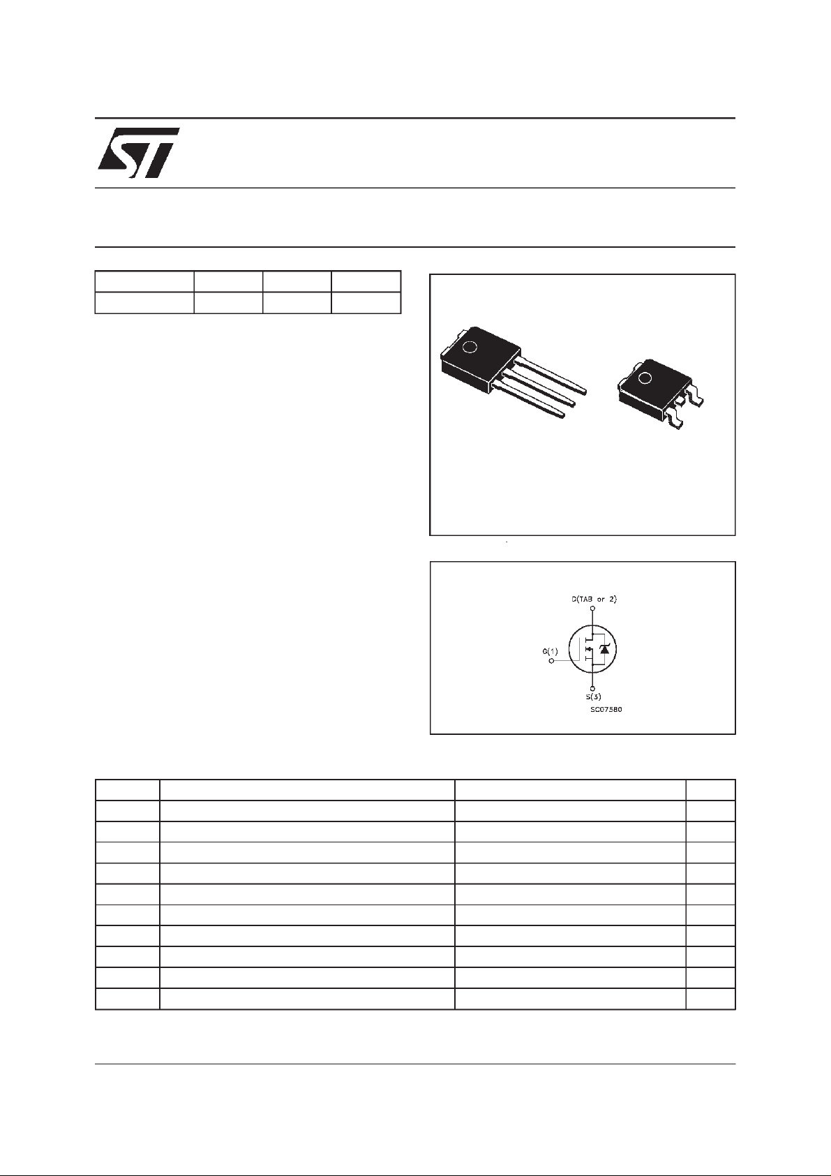
■ THROUGH-HOLEIPAK (TO-251) POWER
PACKAGEIN TUBE(SUFFIX”-1”)
■ SURFACE-MOUNTING DPAK (TO-252)
POWERPACKAGEIN TAPE& REEL
(SUFFIX”T4”)
APPLICATIONS
■ HIGHCURRENT, HIGH SPEEDSWITCHING
■ SOLENOIDAND RELAY DRIVERS
■ DC-DCCONVERTERS & DC-AC INVERTERS
■ TELECOMMUNICATIONPOWERSUPPLIES
INDUSTRIALMOTORDRIVES
3
2
IPAK
TO-251
(Suffix”-1”)
1
(Suffix ”T4”)
1
DPAK
TO-252
INTERNAL SCHEMATIC DIAGRAM
3
ABSOLUTE MAXIMUM RATINGS
Symb o l Parameter Value Unit
V
V
V
I
DM
P
T
(•) Pulse width limited by safe operating area
March 1999
Drain-source Voltage (VGS= 0) 200 V
DS
Drain- gate Voltag e ( RGS=20kΩ) 200 V
DGR
Gate-s ource Voltage
GS
I
Drain Curr ent (continu ous) at Tc=25oC5A
D
I
Drain Curr ent (continu ous) at Tc=100oC 3.5 A
D
20 V
±
(•) Drain Curr ent (pulsed) 20 A
Tot al Dissipat ion at Tc=25oC45W
tot
Derat ing Factor 0.36 W/
Sto rage Tem perature -65 to 150
stg
T
Max. Operat ing Junc tion Tem per ature 150
j
o
o
o
C
C
C
1/10
Page 2
STD5N20
THERMAL DATA
R
thj-case
R
thj-amb
R
thc-sink
T
AVALANCHE CHARACTERISTICS
Symbol Parameter Max Value Unit
I
AR
E
Ther mal Resistanc e Junct ion-case Max
Ther mal Resistanc e Junct ion-ambie nt Max
Ther mal Resistanc e Case-sink Ty p
Maximum Lead Tem pera tu r e For Soldering Purpose
l
Avalanche Current, Repetitive or Not-Repetitive
(pulse width limited by T
Single Pulse A v alan che Ener gy
AS
(starting T
=25oC, ID=IAR,VDD=50V)
j
max,)
j
2.77
100
1.5
275
5A
130 mJ
o
C/W
o
C/W
o
C/W
o
C
ELECTRICAL CHARACTERISTICS
=25oC unless otherwisespecified)
(T
case
OFF
Symbol Parameter Test Conditions Min. Typ. M ax. Unit
V
(BR)DSS
Drain-source
ID=250µAVGS= 0 200 V
Break dow n Volt age
I
DSS
I
GSS
Zero Gate Voltage
Drain Current (V
GS
Gat e- bod y Leakage
Current (V
DS
=0)
=0)
V
=MaxRating
DS
=MaxRating Tc=125oC
V
DS
V
=± 20 V
GS
10
100
100 nA
±
ON(∗)
Symbol Parameter Test Conditions Min. Typ. M ax. Unit
V
GS(th)
R
DS(on)
Gate Threshold Voltage VDS=VGSID= 250 µA 234V
Sta t ic Drain-sour c e On
VGS=10V ID= 2.5 A 0.7 0.8
Resistance
I
D(on)
On State Drain Current VDS>I
D(on)xRDS(on)ma x
5A
VGS=10V
DYNAMIC
Symbol Parameter Test Conditions Min. Typ. M ax. Unit
g
(∗)Forward
fs
Tr ansc on duc tance
C
C
C
Input Capaci tanc e
iss
Out put Capacitance
oss
Reverse Transfer
rss
Capacit a nc e
VDS>I
D(on)xRDS(on)ma xID
=2.5A 1.5 3 S
VDS=25V f=1MHz VGS= 0 450
75
15
600
100
20
µ
µA
Ω
pF
pF
pF
A
2/10
Page 3
STD5N20
ELECTRICAL CHARACTERISTICS
(continued)
SWITCHING ON
Symbol Parameter Test Conditions Min. Typ. M ax. Unit
t
d(on)
t
r
Turn-on Time
Rise T ime
VDD=100V ID=2.5A
R
=4.7
G
Ω
VGS=10V
7
6
10
8
(see test circuit, figure 3)
(di/dt)
Tur n-on Current Slope VDD=160V ID=5A
on
R
G
=47
Ω
VGS=10V
400 A/µs
(see test circuit, figure 5)
Q
Q
Q
Tot al Gate Char ge
g
Gat e- Source Charge
gs
Gate-Drain Charge
gd
VDD= 160 V ID=5A VGS=10V 18
6
7
25 nC
SWITCHING OFF
Symbol Parameter Test Conditions Min. Typ. M ax. Unit
t
r(Voff)
t
t
Off-voltage Ris e Time
Fall T ime
f
Cross-over Tim e
c
VDD=160V ID=5A
=4.7 Ω VGS=10V
R
G
(see test circuit, figure 5)
15
7
5
10
7
20
SOURCEDRAINDIODE
Symbol Parameter Test Conditions Min. Typ. M ax. Unit
I
SD
I
SDM
V
SD
t
Q
I
RRM
(∗) Pulsed:Pulse duration = 300 µs, duty cycle 1.5 %
(•) Pulse width limited by safeoperating area
Source-drain Current
(•)
Source-drain Current
5
20
(pulsed)
(∗)ForwardOnVoltage ISD=5A VGS=0 1.5 V
Reverse Recovery
rr
Time
Reverse Recovery
rr
ISD= 5 A di/dt = 100 A/µs
= 100 V Tj=150oC
V
DD
(see test circuit, figure 5)
180
1125
Charge
Reverse Recovery
12.5
Current
ns
ns
nC
nC
ns
ns
ns
A
A
ns
nC
A
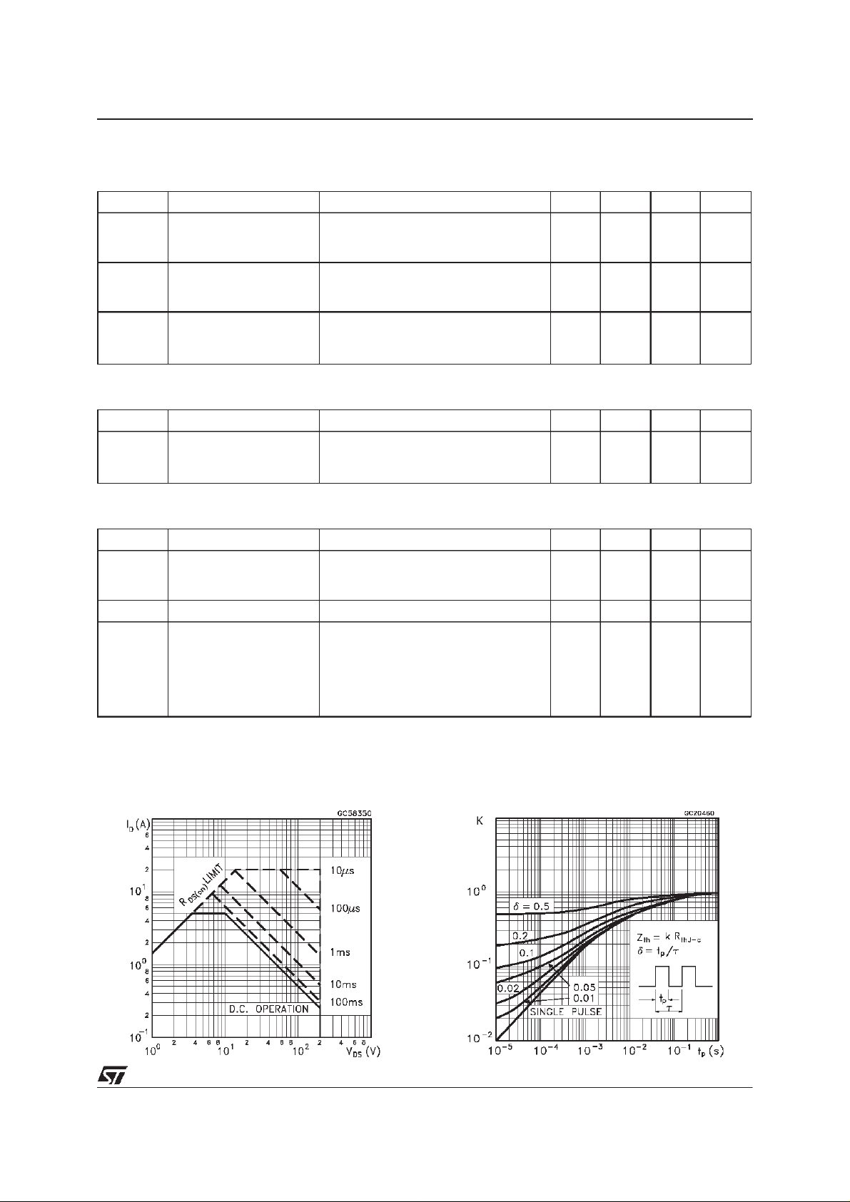
SafeOperating Area ThermalImpedance
3/10
Page 4

STD5N20
DeratingCurve
TransferCharacteristics
OutputCharacteristics
Transconductance
Static Drain-sourceOn Resistance
4/10
Gate Charge vs Gate-sourceVoltage
Page 5

STD5N20
CapacitanceVariations
NormalizedOn Resistancevs Temperature
NormalizedGate ThresholdVoltage vs
Temperature
Turn-onCurrent Slope
Turn-offDrain-source VoltageSlope
Cross-overTime
5/10
Page 6

STD5N20
SwitchingSafe Operating Area
Source-drainDiode Forward Characteristics
AccidentalOverloadArea
Fig. 1:
6/10
UnclampedInductiveLoad TestCircuit
Fig. 2:
UnclampedInductiveWaveform
Page 7

STD5N20
Fig. 3:
SwitchingTimes Test CircuitsFor
ResistiveLoad
Fig. 5: Test Circuit For Inductive Load Switching
AndDIode RecoveryTimes
Fig. 4:
GateCharge test Circuit
7/10
Page 8

STD5N20
TO-251 (IPAK) MECHANICALDATA
DIM.
mm inch
MIN. TYP. MAX. MIN. TYP. MAX.
A 2.2 2.4 0.086 0.094
A1 0.9 1.1 0.035 0.043
A3 0.7 1.3 0.027 0.051
B 0.64 0.9 0.025 0.031
B2 5.2 5.4 0.204 0.212
B3 0.85 0.033
B5 0.3 0.012
B6 0.95 0.037
C 0.45 0.6 0.017 0.023
C2 0.48 0.6 0.019 0.023
D 6 6.2 0.236 0.244
E 6.4 6.6 0.252 0.260
G 4.4 4.6 0.173 0.181
H 15.9 16.3 0.626 0.641
L 9 9.4 0.354 0.370
L1 0.8 1.2 0.031 0.047
L2 0.8 1 0.031 0.039
8/10
A
E
==
C2
L2
B2
==
H
C
A3
A1
B6
L
B
B5
G
==
D
B3
2
13
L1
0068771-E
Page 9

TO-252 (DPAK) MECHANICAL DATA
STD5N20
DIM.
mm inch
MIN. TYP. MAX. MIN. TYP. MAX.
A 2.2 2.4 0.086 0.094
A1 0.9 1.1 0.035 0.043
A2 0.03 0.23 0.001 0.009
B 0.64 0.9 0.025 0.035
B2 5.2 5.4 0.204 0.212
C 0.45 0.6 0.017 0.023
C2 0.48 0.6 0.019 0.023
D 6 6.2 0.236 0.244
E 6.4 6.6 0.252 0.260
G 4.4 4.6 0.173 0.181
H 9.35 10.1 0.368 0.397
L2 0.8 0.031
L4 0.6 1 0.023 0.039
H
A
E
==
C2
L2
B2
==
DETAIL”A”
D
2
13
L4
A1
C
A2
DETAIL”A”
B
G
==
0068772-B
9/10
Page 10

STD5N20
Information furnished is believed tobe accurateand reliable.However, STMicroelectronics assumes no responsibility for the consequences
of use of such information nor for any infringement of patents or other rights of third parties which may result from its use. No license is
granted by implication or otherwise under any patent or patent rights of STMicroelectronics. Specificationmentioned in this publicationare
subjecttochange without notice. This publicationsupersedesandreplaces all information previouslysupplied.STMicroelectronics products
are not authorized for use as critical components in life support devices or systemswithout express written approval of STMicroelectronics.
The STlogo is a trademark ofSTMicroelectronics
1999 STMicroelectronics – Printed in Italy – All Rights Reserved
STMicroelectronics GROUP OF COMPANIES
Australia - Brazil -Canada - China - France - Germany - Italy - Japan - Korea - Malaysia - Malta - Mexico - Morocco - The Netherlands-
10/10
Singapore - Spain - Sweden - Switzerland - Taiwan - Thailand - United Kingdom - U.S.A.
http://www.st.com
.
 Loading...