

Page 1
STD4NC50
N - CHANNEL 500V - 1.3 Ω - 3.7 A TO-251
PowerMESH MOSFET
TYPE V
DSS
R
DS(on)
I
D
ST D4N C50 500 V < 1.5 Ω 3.7 A
■ TYPICALR
■ EXTREMELYHIGH dv/dt CAPABILITY
■ 100%AVALANCHETESTED
■ NEWHIGH VOLTAGE BENCHMARK
■ GATECHARGE MINIMIZED
DS(on)
= 1.3 Ω
DESCRIPTION
The PowerMESHII is the evolution of the first
generation of MESH OVERLAY. The layout
refinements introduced greatly improve the
Ron*areafigure of merit while keeping the device
at the leading edge for what concerns switching
speed,gate chargeand ruggedness.
APPLICATIONS
■ HIGHCURRENT, HIGH SPEED SWITCHING
■ SWITHMODE POWER SUPPLIES(SMPS)
■ DC-AC CONVERTERS FOR WELDING
EQUIPMENTANDUNINTERRUPTIBLE
POWERSUPPLIESAND MOTOR DRIVER
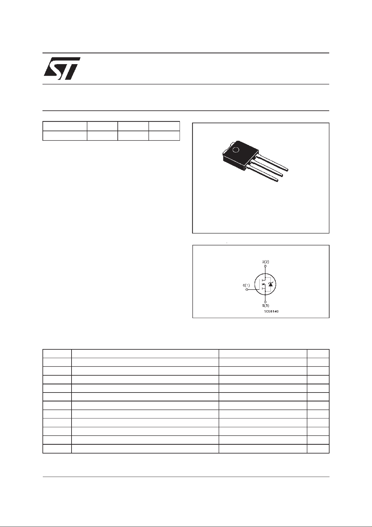
3
2
1
IPAK
TO-251
(Suffix ”-1”)
INTERNAL SCHEMATIC DIAGRAM
ABSOLUTE MAXIMUM RATINGS
Symbol Parameter Value Unit
V
V
V
I
DM
P
dv/dt(
T
(•) Pulse width limited by safe operating area (1)ISD≤3.7 A, di/dt ≤ 100 A/µs, VDD≤ V
September 1999
Dra in- sour c e Volt age (VGS= 0) 500 V
DS
Dra in- gat e V ol t age (RGS=20kΩ) 500 V
DGR
Gat e-source Voltage ± 30 V
GS
Dra in Cu rr ent (contin uous ) a t Tc=25oC3.7A
I
D
Dra in Cu rr ent (contin uous ) a t Tc=100oC2.3A
I
D
(•) Dra in Cu rr ent (pulsed) 14.8 A
Tot al Dis sipation at Tc=25oC50W
tot
Der ati ng Fact or 0.4 W/
1) Peak Di ode Re covery voltage sl ope 3 V/ ns
St orage T em pe r at ure -65 to 150
stg
Max. Operating Junc t ion Tem peratur e 150
T
j
,Tj≤ T
(BR)DSS
JMAX
o
C
o
C
o
C
1/8
Page 2

STD4NC50
THERMAL DATA
R
thj-case
Rthj-a mb
R
thc-sink
T
AVALANCHE CHARACTERISTICS
Symbol Parameter Max Valu e Unit
I
AR
E
Ther mal Resistanc e Junct ion-case Max
Ther mal Resistanc e Junct ion-ambient Max
Ther mal Resistanc e Case-sink Ty p
Maximum Lead Tempera t ure For Soldering Purpose
l
Avalanche Current, Repetitive or Not-Repetitive
(pulse width limited by T
Single Pul se A v alan c he E nergy
AS
(starting T
=25oC, ID=IAR,VDD=50V)
j
max)
j
2.5
100
1.5
275
3.7 A
220 mJ
o
C/W
oC/W
o
C/W
o
C
ELECTRICAL CHARACTERISTICS
=25oC unless otherwisespecified)
(T
case
OFF
Symbol Parameter Test Conditions Min. Typ. Max. Unit
V
(BR)DSS
Drain-source
ID=250µAVGS= 0 500 V
Break dow n Vo lt age
I
DSS
I
GSS
Zero Gate Voltage
Drain Curre nt (V
GS
Gat e- bod y Leakag e
Current (V
DS
=0)
=0)
V
=MaxRating
DS
=MaxRating Tc=125oC
V
DS
V
=± 30 V
GS
1
50
100 nA
±
ON(∗)
Symbol Parameter Test Conditions Min. Typ. Max. Unit
V
GS(th)
R
DS(on)
Gate Threshold Voltage VDS=VGSID= 250 µA 234V
Sta t ic Drain-s our c e On
VGS=10V ID=1.9A 1.3 1.5
Resistance
I
D(on)
On State Drain Current VDS>I
D(on)xRDS(on)ma x
3.7 A
VGS=10V
DYNAMIC
Symbol Parameter Test Conditions Min. Typ. Max. Unit
g
(∗)Forward
fs
Tr ansc on duc tance
C
C
C
Input Capacit anc e
iss
Out put Capac itance
oss
Reverse Transfer
rss
Capacit a nc e
VDS>I
D(on)xRDS(on)ma xID
=1.9A 3 S
VDS=25V f=1MHz VGS= 0 700
85
9
µ
µA
Ω
pF
pF
pF
A
2/8
Page 3
STD4NC50
ELECTRICAL CHARACTERISTICS
(continued)
SWITCHING ON
Symbol Parameter Test Conditions Min. Typ. Max. Unit
t
d(on)
Turn-on Time
t
r
Rise T ime
VDD=250V ID= 1.9 A
=4.7 Ω VGS=10V
R
G
11.5
9
(see test circuit, figure 3)
Q
Q
Q
Tot al Gate Char ge
g
Gat e- Source Charge
gs
Gate-Drain Charge
gd
VDD= 400 V ID=3.7A VGS=10V 18
6
8
25 nC
SWITCHING OFF
Symbol Parameter Test Conditions Min. Typ. Max. Unit
t
r(Voff)
t
t
Off-voltage Ris e Time
Fall T ime
f
Cross-over Time
c
VDD=400V ID= 3.7 A
=4.7 Ω VGS=10V
R
G
(see test circuit, figure 5)
7
6
13
SOURCEDRAINDIODE
Symbol Parameter Test Conditions Min. Typ. Max. Unit
I
SD
I
SDM
V
SD
t
Q
I
RRM
(∗) Pulsed:Pulse duration = 300 µs, duty cycle 1.5 %
(•) Pulse width limited by safeoperating area
Source-drain Current
(•)
Source-drain Current
3.7
14.8
(pulsed)
(∗)ForwardOnVoltage ISD=3.7A VGS=0 1.6 V
Reverse Recovery
rr
Time
Reverse Recovery
rr
ISD= 3.7 A di/dt = 100 A/µs
= 100 V Tj=150oC
V
DD
(see test circuit, figure 5)
380
2.3
Charge
Reverse Recovery
12
Current
ns
ns
nC
nC
ns
ns
ns
A
A
ns
µC
A
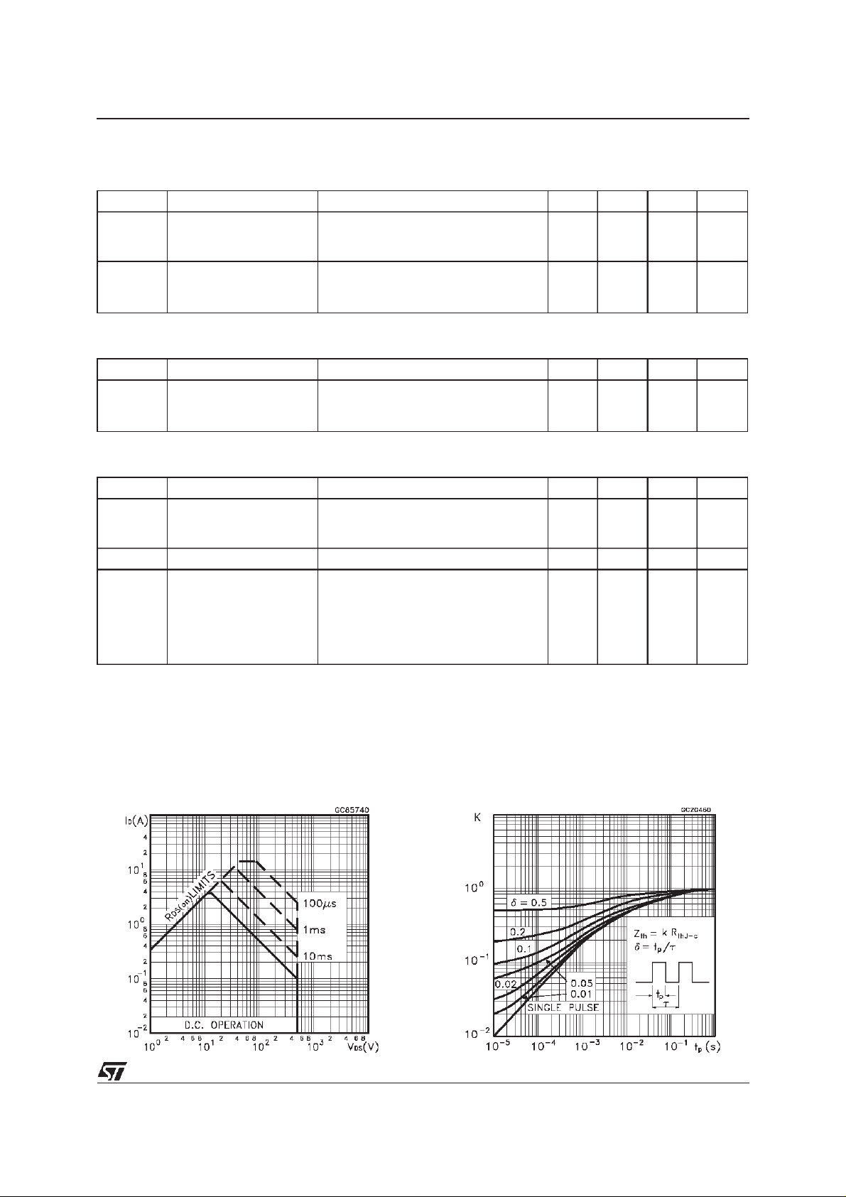
SafeOperating Area ThermalImpedance
3/8
Page 4

STD4NC50
OutputCharacteristics
Transconductance
TransferCharacteristics
Static Drain-sourceOn Resistance
Gate Charge vs Gate-sourceVoltage
4/8
CapacitanceVariations
Page 5

STD4NC50
NormalizedGate ThresholdVoltage vs
Temperature
Source-drainDiode Forward Characteristics
NormalizedOn Resistancevs Temperature
5/8
Page 6

STD4NC50
Fig. 1:
UnclampedInductiveLoad Test Circuit
Fig. 3: SwitchingTimes Test CircuitsFor
ResistiveLoad
Fig. 2:
UnclampedInductive Waveform
Fig. 4: Gate Charge test Circuit
Fig. 5:
Test Circuit For InductiveLoad Switching
And Diode Recovery Times
6/8
Page 7

TO-251 (IPAK) MECHANICALDATA
STD4NC50
DIM.
mm inch
MIN. TYP. MAX. MIN. TYP. MAX.
A 2.2 2.4 0.086 0.094
A1 0.9 1.1 0.035 0.043
A3 0.7 1.3 0.027 0.051
B 0.64 0.9 0.025 0.031
B2 5.2 5.4 0.204 0.212
B3 0.85 0.033
B5 0.3 0.012
B6 0.95 0.037
C 0.45 0.6 0.017 0.023
C2 0.48 0.6 0.019 0.023
D 6 6.2 0.236 0.244
E 6.4 6.6 0.252 0.260
G 4.4 4.6 0.173 0.181
H 15.9 16.3 0.626 0.641
L 9 9.4 0.354 0.370
L1 0.8 1.2 0.031 0.047
L2 0.8 1 0.031 0.039
A
E
==
C2
L2
B2
==
H
C
A3
A1
B6
L
B
B5
G
==
D
B3
2
13
L1
0068771-E
7/8
Page 8

STD4NC50
Information furnished is believed tobe accurateand reliable.However, STMicroelectronics assumes no responsibilityforthe consequences
of use of such information nor for any infringement of patents or other rights of third parties which may result from its use. No license is
granted by implication or otherwise under any patent or patent rights of STMicroelectronics. Specificationmentioned in this publication are
subjecttochange without notice.This publication supersedes and replacesall information previously supplied. STMicroelectronics products
are not authorized for use as critical components in life support devices or systemswithout express written approval of STMicroelectronics.
The STlogo is a trademark ofSTMicroelectronics
1999 STMicroelectronics – Printed in Italy – All Rights Reserved
STMicroelectronics GROUP OF COMPANIES
Australia - Brazil -Canada - China - France - Germany - Italy - Japan - Korea - Malaysia -Malta - Mexico - Morocco - The Netherlands -
8/8
Singapore - Spain - Sweden - Switzerland - Taiwan - Thailand - United Kingdom - U.S.A.
http://www.st.com
.
 Loading...