

Page 1
®
STD4NB25
N - CHANNEL 250V - 0.95Ω - 4A - DPAK/IPAK
PowerMESH MOSFET
PRELIMINARY DATA
TYPE V
DSS
R
DS(on)
I
D
STD4NB25 250 V < 1.1 Ω 4 A
ν TYPICAL R
ν EXTREMELY HIGH dv/dt CAPABILITY
ν 100% AVALANCHE TESTED
ν VERY LOW INTRINS IC CAPA CITA NCE S
ν GATE CHARGE MINIMIZED
ν FOR TROUGH-HOLE VERSION CONTACT
DS(on)
= 0.95 Ω
SALES OFFICE
DESCRIPTION
Using the latest high voltage MESH OVERLAY
process, STMicroelectronics has designed an
advanced family of power MOSFETs with
outstanding performances. The new patent
pending strip layout coupled with the Company’s
proprietary edge termination structure, gives the
lowest R
per area, exceptional avalanche
DS(on)
and dv/dt capabilities and unrivalled gate charge
and switching characteristics.
APPLICATIONS
ν SWITCH M ODE PO W E R SUP PLIE S (S MP S )
ν DC-AC CONVERTERS FOR WELDING
EQUIPME NT AND UNINTERRUP TIBLE
POWE R SUP PLI ES AND MOTO R DRIV E
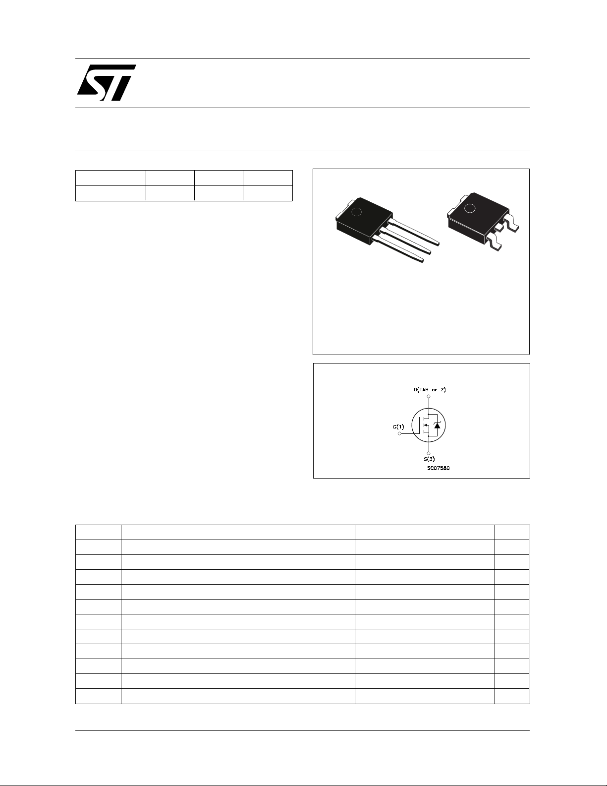
3
2
1
IPAK
TO-251
(Suffix "-1" )
DPAK
TO-252
(Suffix "T4")
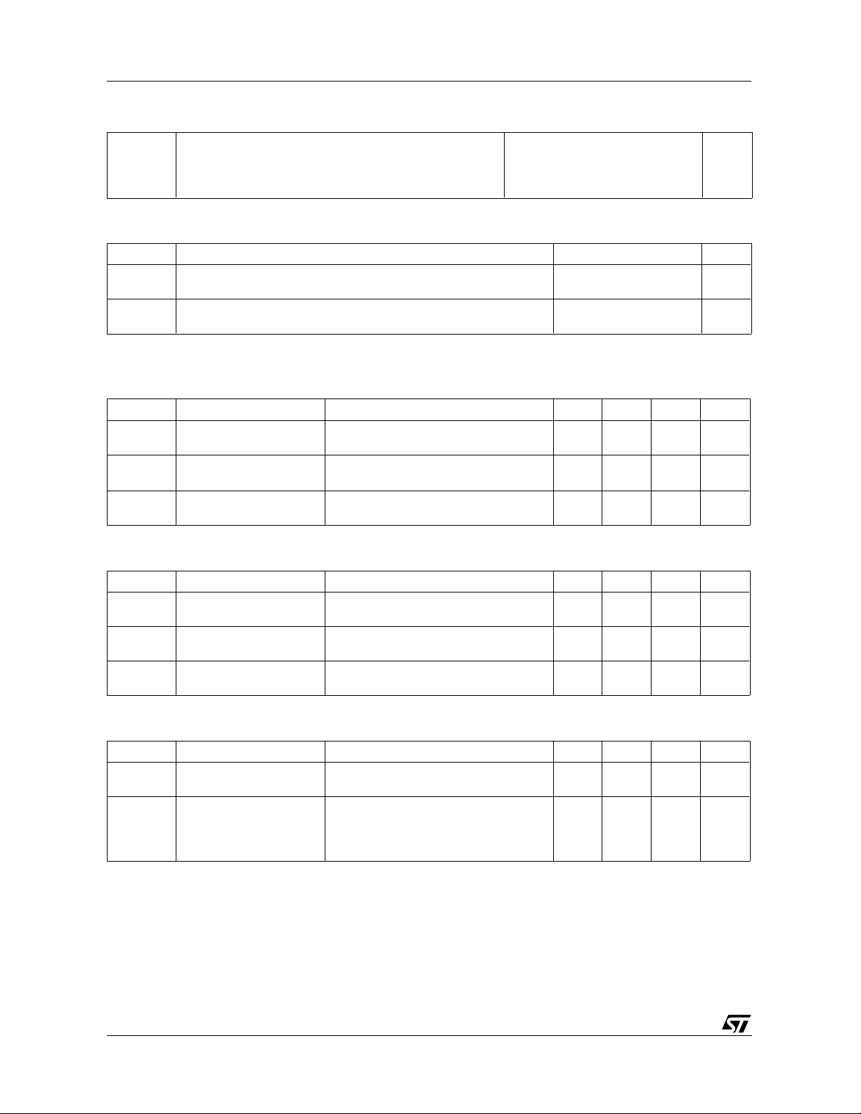
INTERNAL SCHEMATIC DIAGRAM
3
1
ABSOLUTE MAXIMUM RATINGS
Symbol Parameter Value Unit
V
V
V
I
DM
P
dv/dt(
T
(•) Pulse width limited by safe operating area (1) ISD ≤4 Α, di/dt â 20 0 A/µs, VDD ≤ V
February 2000
Drain-source Voltage (VGS = 0) 250 V
DS
Drain- gate Voltage (RGS = 20 kΩ)
DGR
Gate-source Voltage ± 30 V
GS
I
Drain Current (continuous) at Tc = 25 oC4A
D
I
Drain Current (continuous) at Tc = 100 oC2.5A
D
250 V
(•) Drain Current (pulsed) 16 A
Total Dissipation at Tc = 25 oC40W
tot
Derating Factor 0.32 W/oC
1) Peak Diode Recovery voltage slope 5.5 V/ns
Storage Temperature -65 to 150
stg
T
Max. Operating Junction Temperature 150
j
, Tj ≤ T
(BR)DSS
JMAX
o
C
o
C
1/6
Page 2
STD4NB25
THERMAL DATA
R
thj-case
Rthj-amb
R
thc-sink
T
Thermal Resistance Junction-case Max
Thermal Resistance Junction-ambient Max
Thermal Resistance Case-sink Typ
Maximum Lead Temperature For Soldering Purpose
l
AVALANCHE CHARACTERISTICS
Symbol Parameter Max Value Unit
I
AR
E
Avalanche Current, Repetitive or Not-Repetitive
(pulse width limited by T
Single Pulse Avalanche Energy
AS
(starting T
= 25 oC, ID = IAR, V
j
max)
j
DD
= 50 V)
3.12
100
1.5
275
4A
75 mJ
o
C/W
oC/W
o
C/W
o
C
ELECTRICAL CHARACTERISTICS (T
= 25 oC unless otherwise specified)
case
OFF
Symbol Parameter Test Conditions Min. Typ. Max. Unit
V
(BR)DS S
Drain-source
I
= 250 µA V
D
GS
= 0
250 V
Breakdown Voltage
I
DSS
I
GSS
Zero Gate Voltage
Drain Current (V
GS
Gate-body Leakage
Current (V
DS
= 0)
= 0)
= Max Rating
V
DS
V
= Max Rating Tc = 125 oC
DS
V
= ± 30 V
GS
1
10
± 100 nA
ON (∗)
Symbol Parameter Test Conditions Min. Typ. Max. Unit
V
GS(th)
Gate Threshold
V
= VGS ID = 250 µA
DS
345V
Voltage
R
DS(on)
Static Drain-source On
VGS = 10V ID =2 A 0.9 5 1.1 Ω
Resistance
I
D(on)
On State Drain Current VDS > I
V
= 10 V
GS
D(on)
x R
DS(on)max
4A
DYNAMIC
Symbol Parameter Test Conditions Min. Typ. Max. Unit
g
(∗) Forward
fs
Transconductance
C
C
C
Input Capacitance
iss
Output Capacitance
oss
Reverse Transfer
rss
Capacitance
VDS > I
V
DS
x R
D(on)
DS(on)max
= 25 V f = 1 MHz V
ID =2 A 0.7 1.6 S
= 0 260
GS
70
350
100
9
13
µA
µA
pF
pF
pF
2/6
Page 3

STD4NB25
ELECTRICAL CHARACTERISTICS (continued)
SWITC H ING ON
Symbol Parameter Test Conditions Min. Typ. Max. Unit
t
d(on)
t
r
Turn-on Time
Rise Time
V
= 125 V ID = 3 A
DD
= 4.7 Ω VGS = 10 V
R
G
9
9
13
13
ns
ns
Q
Q
Q
Total Gate Charge
g
Gate-Source Charge
gs
Gate-Drain Charge
gd
VDD = 200 V ID = 6 A V
= 10 V 12
GS
17 nC
7.5
3
SWITC H ING OFF
Symbol Parameter Test Conditions Min. Typ. Max. Unit
t
r(Voff)
t
t
Off-voltage Rise Time
Fall Time
f
Cross-over Time
c
V
= 200 V ID = 6 A
DD
RG = 4.7 Ω VGS = 10 V
8
7
15
11
10
20
SOURCE DRAIN DIODE
Symbol Parameter Test Conditions Min. Typ. Max. Unit
4
16
I
SDM
I
SD
Source-drain Current
(•)
Source-drain Current
(pulsed)
V
(∗) Forward On Voltage ISD = 6 A VGS = 0 1.5 V
SD
t
Q
Reverse Recovery
rr
Time
Reverse Recovery
rr
I
= 6 A di/dt = 100 A/µs
SD
V
= 100 V Tj = 150 oC
DD
160
720
Charge
I
RRM
Reverse Recovery
9
Current
(∗) Pulsed: Pulse duration = 300 µs, duty cycle 1.5 %
(•) Pulse width limited by safe operating area
nC
nC
ns
ns
ns
A
A
ns
nC
A
3/6
Page 4

0068771-E
STD4NB25
TO-251 (IPAK) MECHANICAL DAT A
DIM.
mm inch
MIN. TYP. MAX. MIN. TYP. MAX.
A 2.2 2.4 0.086 0.094
A1 0.9 1.1 0.035 0.043
A3 0.7 1.3 0.027 0.051
B 0.64 0.9 0.025 0.031
B2 5.2 5.4 0.204 0.212
B3 0.85 0.033
B5 0.3 0.012
B6 0.95 0.037
C 0.45 0.6 0.017 0.023
C2 0.48 0.6 0.019 0.023
D 6 6.2 0.236 0.244
E 6.4 6.6 0.252 0.260
G 4.4 4.6 0.173 0.181
H 15.9 16.3 0.626 0.641
L 9 9.4 0.354 0.370
L1 0.8 1.2 0.031 0.047
L2 0.8 1 0.031 0.039
H
4/6
A
C2
L2
E
B2
= =
= =
D
B3
2
1 3
L1
A1
L
B6
C
A3
B
B5
G
= =
Page 5

TO-252 (DPAK) MECHANICAL DATA
STD4NB25
DIM.
mm inch
MIN. TYP. MAX. MIN. TYP. MAX.
A 2.2 2.4 0.086 0.094
A1 0.9 1.1 0.035 0.043
A2 0.03 0.23 0.001 0.009
B 0.64 0.9 0.025 0.035
B2 5.2 5.4 0.204 0.212
C 0.45 0.6 0.017 0.023
C2 0.48 0.6 0.019 0.023
D 6 6.2 0.236 0.244
E 6.4 6.6 0.252 0.260
G 4.4 4.6 0.173 0.181
H 9.35 10.1 0.368 0.397
L2 0.8 0.031
L4 0.6 1 0.023 0.039
A
C2
L2
E
B2
==
H
DETAIL "A"
D
==
C
B
2
1 3
L4
A1
G
==
A2
DETAIL "A"
0068772-B
5/6
Page 6

STD4NB25
Information f urnished i s believed t o be accurate an d reliabl e. How ever, STMicroelect ronics assu mes no responsib ility fo r the consequen ces
of use of such information nor for any infringement of patents or other rights of third parties which may result from its use. No license is
granted by implication or otherwise under any patent or patent rights of STMicroelectronics. Specification mentioned in this publication are
subject to chan ge w ithout notice. This publicatio n su persedes a nd r eplaces al l inf ormati on previ ously suppl ied. STMicroelect ron ics produ cts
are not auth ori zed f or use as critical compon ents i n life sup port devices or systems without express writte n approval of STMicroelectronics.
The ST logo is a trademark of STMicroelectronics
© 1999 STMicroelectronics – Prin ted in Italy – All Rights Reserved
STMicroele ct ronics GROUP OF COMPANI ES
Australia - Brazil - China - Finland - France - Germany - Hong Kong - India - Italy - Japan - Malaysi a - Malta - Morocco -
6/6
Singapore - Spain - Sweden - Switzerland - United Kingdom - U.S.A.
http://www.st.com
.
 Loading...