

Page 1
STD4N20
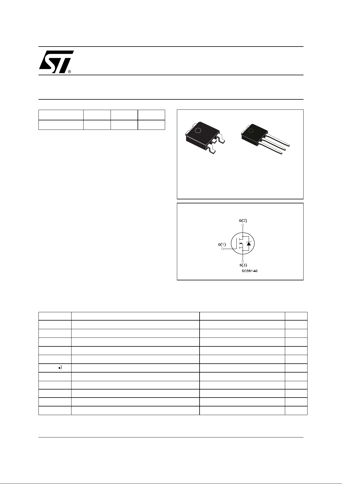
N-CHANNEL 200V - 1.2Ω - 4A DPAK/IPAK
MESH OVERLAY™ MOSFET
TYPE V
DSS
R
DS(on)
I
D
STD4N20 200 V < 1.5 Ω 4 A
■ TYPICAL R
■ EXTREMELY HIGH dv /d t C APABILITY
■ 100% AVALANCHE TESTED
■ ADD SUFFIX “T4” FO R OREDERING IN TAPE &
(on) = 1.2 Ω
DS
REEL
DESCRIPTION
Using the latest high voltage MESH OVERLAY™
process, STMicroelectronics has designed an advanced family of power MOSFETs with outstanding
performance. The new patented STrip layout coupled with the Company’s proprietary edge termination structure, makes it suitable in coverters for
lighting applications.
APPLICATIONS
■ HIGH CURRENT, HIGH SPEED SWITCHING
■ SWITH MODE POWER SUPPLI ES ( SMPS)
■ DC-DC CONVERTERS FOR TELECOM,
INDUSTRIAL, AND LIGHTING EQUIPMENT
3
1
DPAK
TO-252
INTERNAL SCHEMATIC DIAGRAM
IPAK
TO-251
3
2
1
ABSOLUTE MAXIMUM RATINGS
Symbol Parameter Value Unit
V
DS
V
DGR
V
GS
I
D
I
D
I
DM
P
TOT
dv/dt (1) Peak Diode Recovery voltage slope 5 V/ns
T
stg
T
j
(•)Pu l se width limited by safe operating area
Drain-source Voltage (VGS = 0)
Drain-gate Voltage (RGS = 20 kΩ)
200 V
200 V
Gate- source Voltage ±20 V
Drain Current (continuous) at TC = 25°C
Drain Current (continuous) at TC = 100°C
(l)
Drain Current (pulsed) 16 A
Total Dissipation at TC = 25°C
4A
2.5 A
40 W
Derating Factor 0.32 W/°C
Storage Temperature –65 to 150 °C
Max. Operating Junction Temperature 150 °C
(1)ISD ≤4A, di/dt ≤300A/µs, VDD ≤ V
(BR)DSS
, Tj ≤ T
JMAX.
1/9February 2001
Page 2
STD4N20
THERMA L D ATA
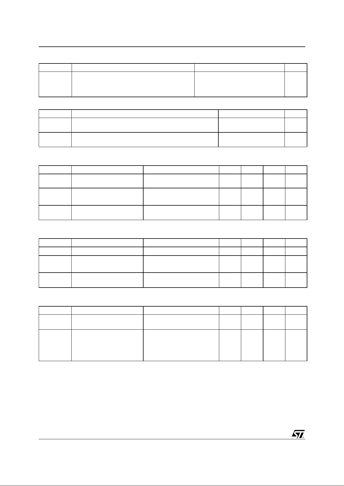
Rthj-case Thermal Resistance Junction-case Max 3.12 °C/W
Rthj-amb Thermal Resistance Junction-ambient Max 100 °C/W
Rthc-sink Thermal Resistance Case-sink Typ 1.5 °C/W
T
l
AVALANCHE CHARACTERISTICS
Symbol Parameter Max Value Unit
I
AR
E
AS
Maximum Lead Temperature For Soldering Purpose 275 °C
Avalanche Current, Repetitive or Not-Repetitive
(pulse width limited by T
max)
j
Single Pulse Avalanche Energy
(starting T
= 25 °C, ID = IAR, VDD = 50 V)
j
4A
76 mJ
ELECTRICAL CHARACTERISTICS (T
= 25 °C UNLESS OTHERWISE SPECIFIED)
CASE
OFF
Symbol Parameter Test Conditions Min. Typ. Max. Unit
V
(BR)DSS
Drain-source
ID = 250 µA, VGS = 0 200 V
Breakdown Voltage
ON
I
I
GSS
(1)
DSS
Zero Gate Voltage
Drain Current (V
GS
Gate-body Leakage
Current (V
DS
= 0)
= 0)
= Max Rating
V
DS
V
= Max Rating, TC = 125 °C
DS
V
= ±20V ±100 nA
GS
1µA
10 µA
Symbol Parameter Test Conditions Min. Typ. Max. Unit
V
V
GS(th)
R
DS(on)
Gate Threshold Voltage
Static Drain-source On
= VGS, ID = 250µA
DS
VGS = 10V, ID = 2 A
234V
1.2 1.5 Ω
Resistance
I
D(on)
On State Drain Current VDS > I
D(on)
x R
DS(on)max,
4A
VGS=10V
DYNAMIC
Symbol Parameter Test Conditions Min. Typ. Max. Unit
(1) Forward Transconductance VDS > I
g
fs
C
iss
C
oss
C
rss
Input Capacitance
Output Capacitance 40 pF
Reverse Transfer
Capacitance
ID=2A
V
DS
D(on)
x R
DS(on)max,
= 25V, f = 1 MHz, VGS = 0
2.7 S
206 pF
16 pF
2/9
Page 3
STD4N20
ELECTRICAL CHARACTERISTICS (CONTINUED)
SWITCHING ON
Symbol Parameter Test Conditions Min. Typ. Max. Unit
V
t
d(on)
t
r
Q
g
Q
gs
Q
gd
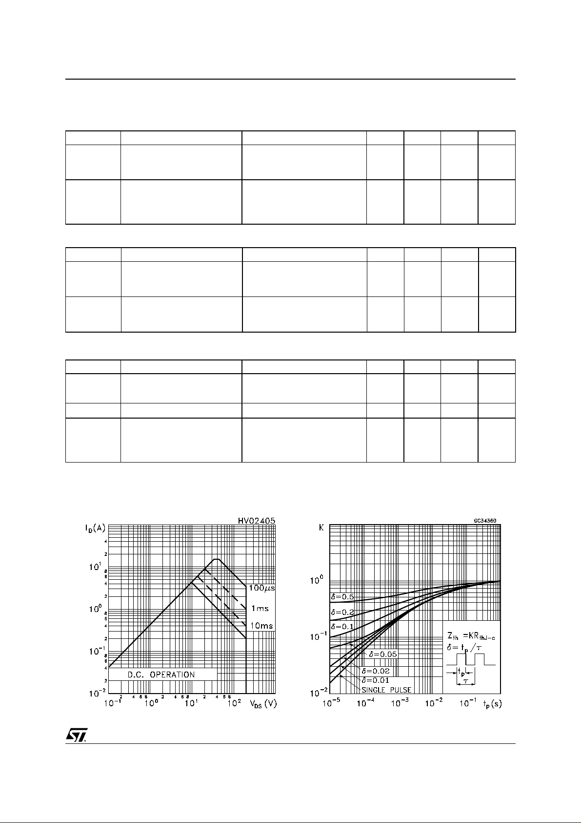
Turn-on Delay Time
Rise Time 10 ns
Total Gate Charge
Gate-Source Charge 2.8 nC
Gate-Drain Charge 4 nC
SWITCHING OFF
Symbol Parameter Test Conditions Min. Typ. Max. Unit
t
d(Voff)
t
t
r(Voff)
t
t
f
f
c
Turn-off- Delay Time
Fall Time
Off-voltage Rise Time
Fall Time
Cross-over Time
SOURCE DRAIN DIODE
Symbol Parameter Test Conditions Min. Typ. Max. Unit
I
SD
I
SDM
VSD (1)
t
rr
Q
rr
I
RRM
Note: 1. Pulsed: Pu l se duration = 300 µs, duty cycle 1.5 %.
2. Pulse width li mited by safe operating ar ea.
Source-drain Current 4 A
(2)
Source-drain Current (pulsed) 16 A
Forward On Voltage
Reverse Recovery Time
Reverse Recovery Charge 446 nC
Reverse Recovery Current 7.2 A
= 100 V, ID = 2 A
DD
RG= 4.7Ω VGS = 10 V
(see test circuit, Figure 3)
V
= 160V, ID = 4 A,
DD
VGS = 10V
VDD = 100V, ID = 2 A,
RG=4.7Ω, V
GS
= 10V
(see test circuit, Figure 3)
V
= 160V, ID = 4 A,
clamp
R
=4.7Ω, V
G
GS
= 10V
(see test circuit, Figure 5)
ISD = 4 A, VGS = 0
I
= 4 A, di/dt = 100A/µs
SD
VDD = 30V, Tj = 150°C
(see test circuit, Figure 5)
9ns
11.2 15.7 nC
26
8
11
6
9
1.5 V
124 ns
ns
ns
ns
ns
ns
Safe Operating Area
Thermal Impedance
3/9
Page 4
STD4N20
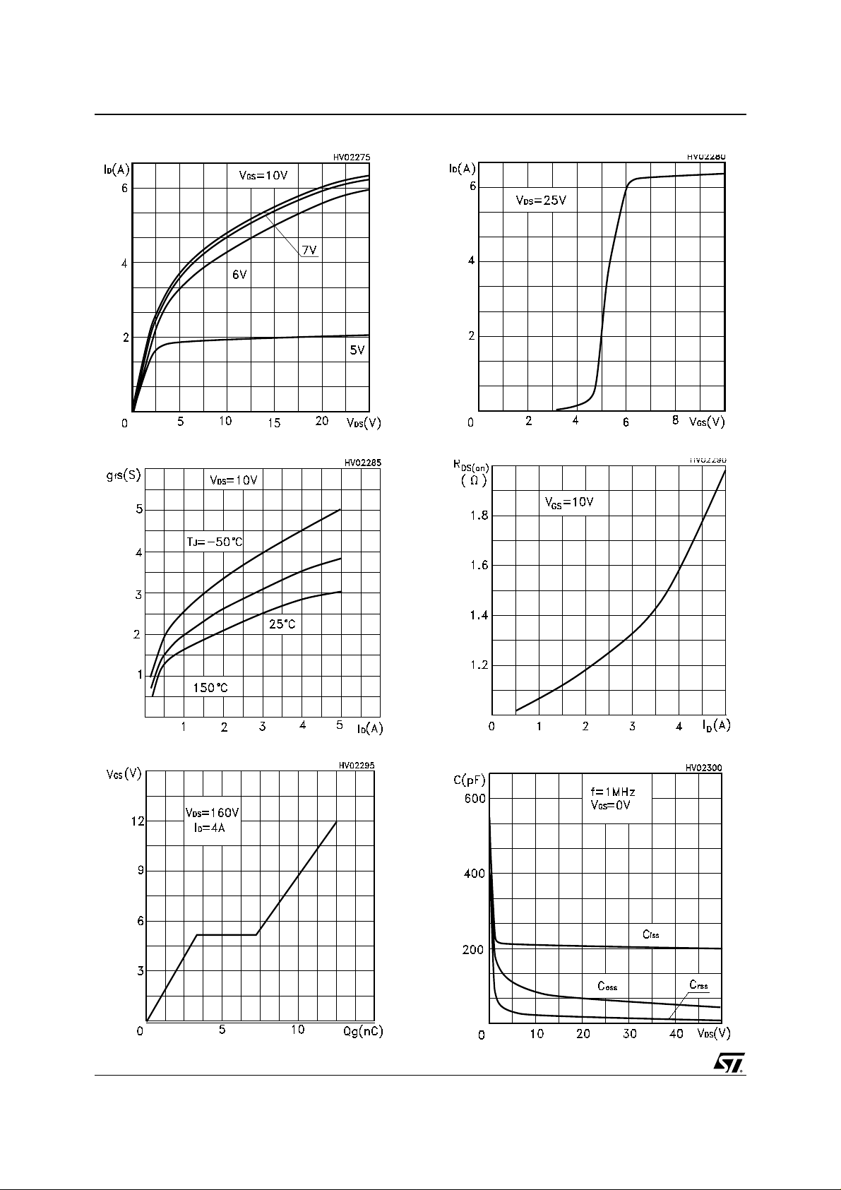
Output Characteristics
Tranconductance
Tranfer Characteristics
Static Drain-Source On Resistance
Gate Charge vs Gate-source Voltage Capacitance Variations
4/9
Page 5
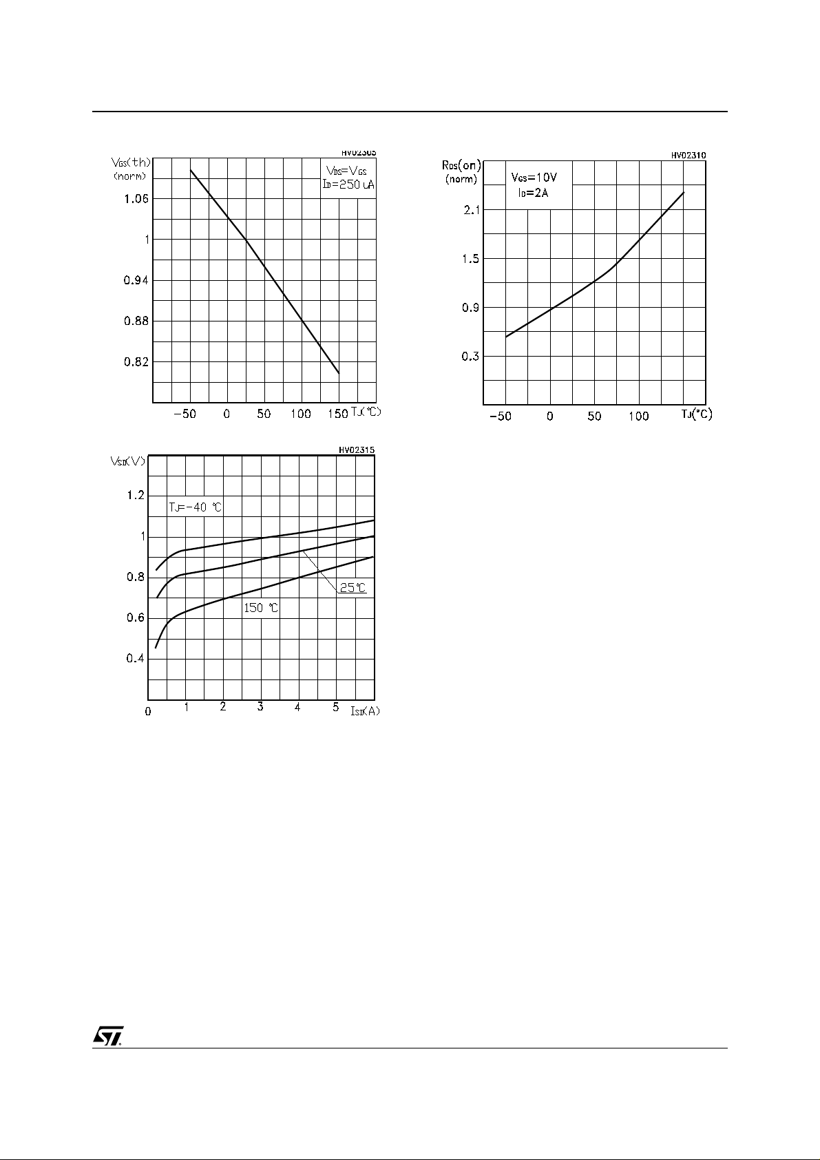
Source-drain Diode Forward Characteristics
STD4N20
Normalized On Resistance vs Temperatur eNormalized Gate Thereshold Voltage vs Temp.
5/9
Page 6
STD4N20
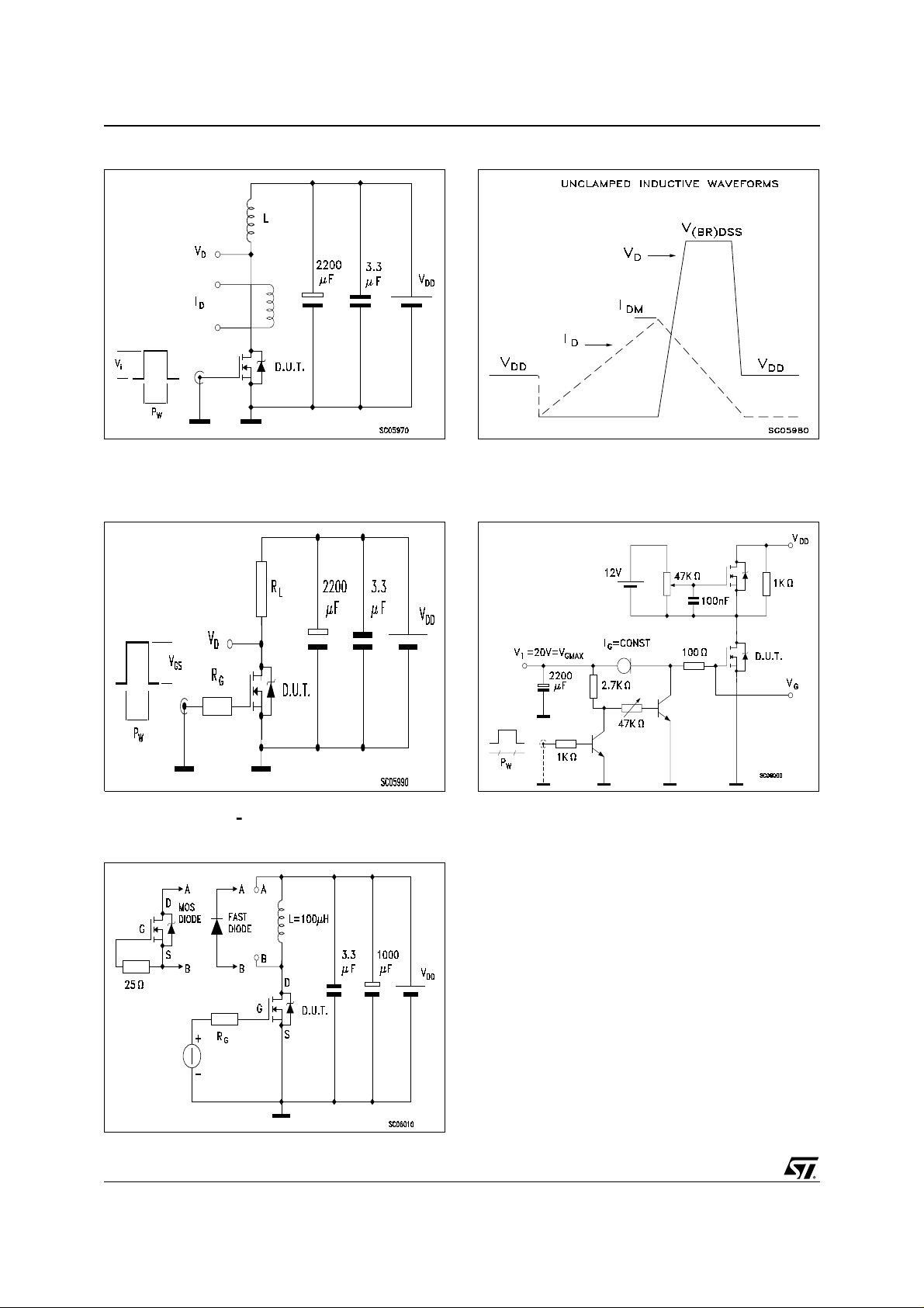
Fig. 2: Unclamped Inductive WaveformFig. 1: Unclamped Inductive Load Test Circuit
Fig. 3: Switching Times Test Circuit For
Resistive Load
Fig. 5: Test Circuit For Inductive Load Switching
And Diode Recovery Times
Fig. 4: Gate Charge test Circuit
6/9
Page 7
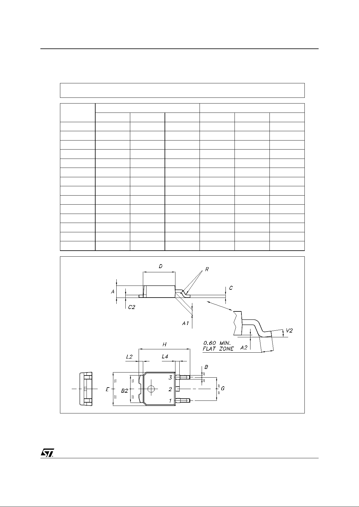
TO-252 (DPAK) MECHANICAL DATA
STD4N20
DIM.
A 2.20 2.40 0.087 0.094
A1 0.90 1.10 0.035 0.043
A2 0.03 0.23 0.001 0.009
B 0.64 0.90 0.025 0.035
B2 5.20 5.40 0.204 0.213
C 0.45 0.60 0.018 0.024
C2 0.48 0.60 0.019 0.024
D 6.00 6.20 0.236 0.244
E 6.40 6.60 0.252 0.260
G 4.40 4.60 0.173 0.181
H 9.35 10.10 0.368 0.398
L2 0.8 0.031
L4 0.60 1.00 0.024 0.039
V2 0
MIN. TYP. MAX. MIN. TYP. MAX.
o
mm inch
o
8
o
0
o
0
P032P_B
7/9
Page 8
STD4N20
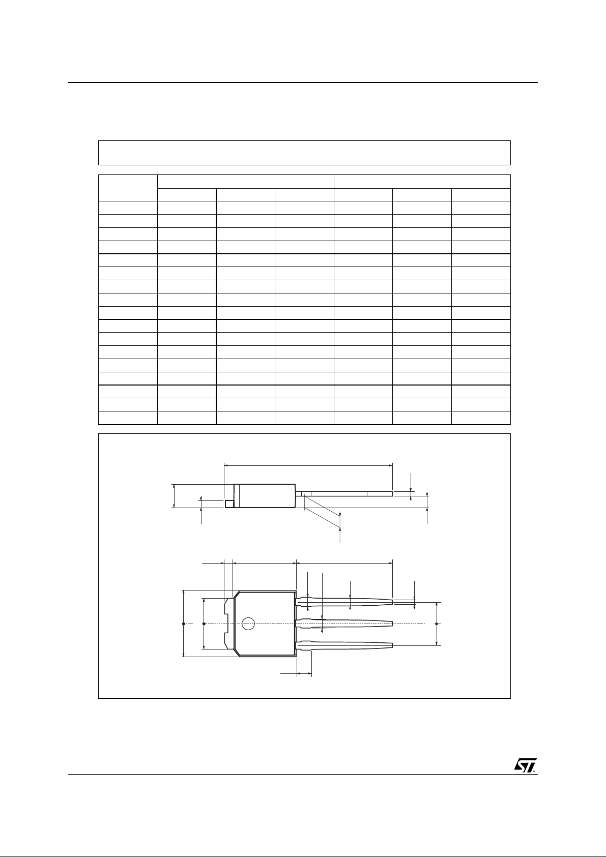
TO-251 (IPAK) MECHANICAL DAT A
DIM.
MIN. TYP. MAX. MIN. TYP. MAX.
mm inch
A 2.2 2.4 0.086 0.094
A1 0.9 1.1 0.035 0.043
A3 0.7 1.3 0.027 0.051
B 0.64 0.9 0.025 0.031
B2 5.2 5.4 0.204 0.212
B3 0.85 0.033
B5 0.3 0.012
B6 0.95 0.037
C 0.45 0.6 0.017 0.023
C2 0.48 0.6 0.019 0.023
D 6 6.2 0.236 0.244
E 6.4 6.6 0.252 0.260
G 4.4 4.6 0.173 0.181
H 15.9 16.3 0.626 0.641
L 9 9.4 0.354 0.370
L1 0.8 1.2 0.031 0.047
L2 0.8 1 0.031 0.039
H
8/9
A
C2
L2
E
B2
= =
= =
D
B3
2
1 3
L1
A1
L
B6
C
A3
B
B5
G
= =
0068771-E
Page 9

STD4N20
Information furnished is believed to be accurate and reliable. However, STMicroelectronics assumes no responsibi lity f or the
consequences of use of su ch in formation nor for any in fringement of paten ts or o ther rights of third parties w hich may result from
its use. No license is granted by implication or otherwise under any patent or patent rights of STMicroelectronics. Specifications
mentioned in this publication are subject to change without notice. This publication supersedes and replaces all information
previously suppli ed. STMi croelect ronics pr oducts are not author ized for use as c ritical component s in li fe suppo rt devi ces or
systems without express written approval of STMicroelectronics.
Australia - Brazil - Canada - China - Finland - France - Germany - Hong Kong - India - Israel - Italy - Japan - Malaysia - Malta - Morocco
© The ST logo is a registered trademark of STMicroelectronics
© 2002 STMicroelectronics - Printed in Italy - All Rights Reserved
Singapore - Spain - Sweden - Switzerland - United Kingdom - United States.
STMicroelectronics GROUP OF COMPANIES
© http://www.st.com
9/9
 Loading...