

Page 1
STD40NF03L
N-CHANNEL 30V - 0.012
LOW GATE CHARGE STripFET POWER MOSFET
TYPE V
ST D40N F 03L 30 V < 0.014 Ω 40 A
■ TYPICALR
■ TYPICALQ
■ OPTIMAL R
■ CONDUCTIONLOSSESREDUCED
■ SWITCHINGLOSSESREDUCED
DS(on)
g
DSS
= 0.012 Ω
= 35 nC @ 10V
DS(on)xQg
DESCRIPTION
This applicationspecific Power Mosfet is the third
generation of STMicroelectronics unique ”Single
Feature Size” strip-based process. The resulting transistor shows the best trade-off between
on-resistance and gate charge. When used as
high and low side in buck regulators, it gives the
best performancein termsof both conductionand
switching losses. This is extremely important for
motherboardswhere fast switching and high efficiencyare of paramount importance.
R
DS(on)
TRADE-OFF
I
D
Ω
- 40A DPAK
PRELIMINARY DATA
3
1
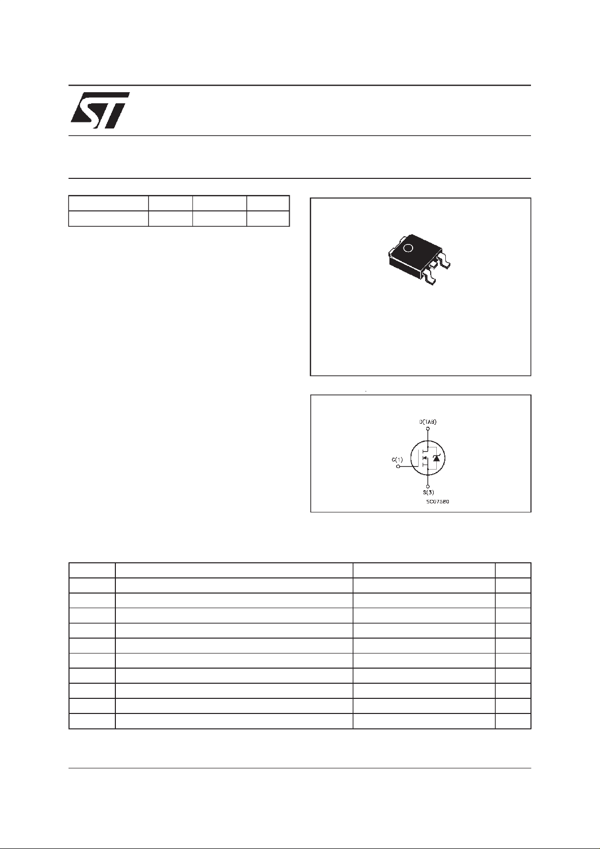
DPAK
TO-252
(Suffix ”T4”)
ADD SUFFIX ”T4” FOR ORDERING IN TAPE & REEL
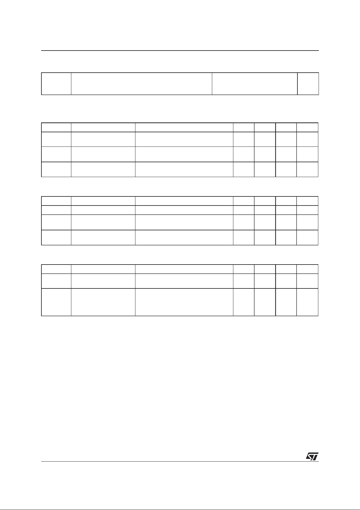
INTERNAL SCHEMATIC DIAGRAM
APPLICATIONS
■ SPECIFICALLYDESIGNED AND
OPTIMISEDFOR HIGH EFFICIENCYCPU
CORE DC/DC CONVERTERS
ABSOLUTE MAXIMUM RATINGS
Symbol Parameter Value Unit
V
V
V
I
D
I
DM
P
T
(•) Current Limited By The Package
(••) Pulse width limited by safe operating area
Dra in- sour c e Volt age (VGS=0) 30 V
DS
Dra in- gate V ol t age ( RGS=20kΩ)30V
DGR
Gat e-source Voltage
GS
(•) Dra in C u rr ent (c ontinuous) a t Tc=25oC20A
I
Dra in C u rr ent (c ontinuous) a t Tc=100oC20A
D
(••) Dra in C u rr ent (puls ed ) 80 A
Tot al Dissipation at Tc=25oC55W
tot
Der ati ng Fac t or 0.37 W/
St orage Temperature -65 t o 175
stg
T
Max. O perating Junction T emper at ure 175
j
20 V
±
o
C
o
C
o
C
14/01/2000
1/6
Page 2
STD40NF03L
THERMAL DATA
R
thj-case
R
thj-amb
T
Ther mal Resistanc e Junct ion-case Max
Ther mal Resistanc e Junct ion-ambient Max
Maximum Lead Te m pe ra tur e For So lder ing Purpose
l
2.73
62.5
300
o
C/W
o
C/W
o
C
ELECTRICAL CHARACTERISTICS
=25oC unless otherwisespecified)
(T
case
OFF
Symbol Parameter Test Condit ions Min. Typ. M ax. Unit
V
(BR)DSS
Drain-source
ID=250µAVGS=0 30 V
Break dow n V o lt age
I
DSS
I
GSS
Zero Gate Voltage
Drain Cur re nt ( V
GS
Gat e- bod y L eakage
Current (V
DS
=0)
=0)
V
=MaxRating
DS
=MaxRating Tc=125oC
V
DS
V
= ± 20 V ± 100 nA
GS
1
10
ON(∗)
Symbol Parameter Test Condit ions Min. Typ. Max. Unit
V
GS(th)
R
DS(on)
I
D(on)
Gate Threshold Voltage VDS=VGSID= 250 µA12.5V
Sta t ic Drain -s ource On
Resistance
On State Drain Current VDS>I
VGS=10V ID=20A
V
=5V ID=20A
GS
D(on)xRDS(on)ma x
0.012
0.019
0.014
0.022
40 A
VGS=10V
DYNAMIC
Symbol Parameter Test Condit ions Min. Typ. Max. Unit
g
(∗)Forward
fs
Tr ansc on duc tance
C
C
C
Input Capac i t ance
iss
Out put Capacitanc e
oss
Reverse Tr ansfer
rss
Capacit a nc e
VDS>I
D(on)xRDS(on)ma xID
=20 A 40 S
VDS=25V f=1MHz VGS= 0 1470
490
110
µA
µ
Ω
Ω
pF
pF
pF
A
2/6
Page 3

STD40NF03L
ELECTRICAL CHARACTERISTICS
(continued)
SWITCHINGON
Symbol Parameter Test Condit ions Min. Typ. Max. Unit
t
d(on)
t
Tur n-on Delay Tim e
Rise Ti me
r
VDD=15V ID=20A
R
=4.7
G
Ω
VGS=4.5V
20
170
(Resis t iv e Loa d, s ee fig. 3)
Q
Q
Q
Tot al Gat e Charge
g
Gat e- Source Charge
gs
Gate-Drain Charge
gd
VDD=24V ID=40A VGS=10V 35
5
10
45 nC
SWITCHINGOFF
Symbol Parameter Test Condit ions Min. Typ. Max. Unit
t
d(off)
Tur n-of f Delay Tim e
t
Fall T ime
f
VDD=15V ID=20A
=4.7 Ω VGS=4.5V
R
G
40
60
(Resis t iv e Loa d, s ee fig. 3)
SOURCEDRAINDIODE
Symbol Parameter Test Condit ions Min. Typ. Max. Unit
I
SD
I
SDM
V
SD
t
Q
I
RRM
(∗) Pulsed:Pulse duration= 300µs, duty cycle 1.5%
(•) Pulse width limited by safe operatingarea
Source-drain Current
(•)
Source-drain Current
20
80
(pulsed)
(∗)ForwardOnVoltage ISD=20 A VGS=0 1.5 V
Reverse Recovery
rr
Time
Reverse Recovery
rr
ISD= 20 A di/dt = 100 A /µ s
=15V Tj=150oC
V
DD
(see test circuit, fig. 5)
70
105
Charge
Reverse Recovery
2.4
Current
ns
ns
nC
nC
ns
ns
A
A
ns
nC
A
3/6
Page 4

STD40NF03L
Fig. 1:
UnclampedInductiveLoad Test Circuit
Fig. 3: SwitchingTimes Test Circuits For
ResistiveLoad
Fig. 2:
UnclampedInductive Waveform
Fig. 4: Gate Chargetest Circuit
Fig. 5:
Test CircuitFor InductiveLoad Switching
And Diode Recovery Times
4/6
Page 5

TO-252 (DPAK) MECHANICAL DATA
STD40NF03L
DIM.
mm inch
MIN. TYP. MAX. MIN. TYP. MAX.
A 2.2 2.4 0.086 0.094
A1 0.9 1.1 0.035 0.043
A2 0.03 0.23 0.001 0.009
B 0.64 0.9 0.025 0.035
B2 5.2 5.4 0.204 0.212
C 0.45 0.6 0.017 0.023
C2 0.48 0.6 0.019 0.023
D 6 6.2 0.236 0.244
E 6.4 6.6 0.252 0.260
G 4.4 4.6 0.173 0.181
H 9.35 10.1 0.368 0.397
L2 0.8 0.031
L4 0.6 1 0.023 0.039
H
A
E
C2
L2
B2
==
==
DETAIL”A”
D
2
13
L4
A1
C
A2
DETAIL”A”
B
G
==
0068772-B
5/6
Page 6

STD40NF03L
Information furnishedis believed tobeaccurateand reliable.However, STMicroelectronics assumes no responsibilityforthe consequences
of use of such information nor for any infringement of patents or other rights of third parties which may result from its use. No license is
granted by implication or otherwise under any patent or patent rights of STMicroelectronics. Specificationmentioned in this publicationare
subjecttochange without notice.This publication supersedes andreplacesall information previously supplied. STMicroelectronics products
are not authorized for use as critical components in life support devices or systemswithout express written approval of STMicroelectronics.
The STlogo is a trademark of STMicroelectronics
1999 STMicroelectronics – Printed in Italy – All Rights Reserved
STMicroelectronics GROUP OF COMPANIES
Australia - Brazil - China - Finland - France - Germany - Hong Kong - India - Italy - Japan - Malaysia - Malta - Morocco -
6/6
Singapore - Spain - Sweden - Switzerland - United Kingdom - U.S.A.
http://www.st.com
.
 Loading...