

Page 1
STD40NF02L
N-CHANNEL 20V - 0.01
LOW GATE CHARGE STripFET POWER MOSFET
TYPE V
ST D40N F 02L 20 V < 0. 013 Ω 40 A
■ TYPICALR
■ TYPICALQ
■ OPTIMAL R
■ CONDUCTIONLOSSESREDUCED
■ SWITCHINGLOSSESREDUCED
DS(on)
g
DSS
= 0.01 Ω
= 35 nC @ 10V
DS(on)xQg
DESCRIPTION
This application specific Power Mosfet is the third
generation of STMicroelectronics unique ”Single
Feature Size” strip-based process. The resulting transistor shows the best trade-off between
on-resistance and gate charge. When used as
high and low side in buck regulators, it gives the
best performancein termsof both conductionand
switching losses. This is extremely important for
motherboardswhere fast switching and high efficiencyare ofparamountimportance.
R
DS(on)
TRADE-OFF
I
D
Ω
- 40A DPAK
TARGET DATA
3
1
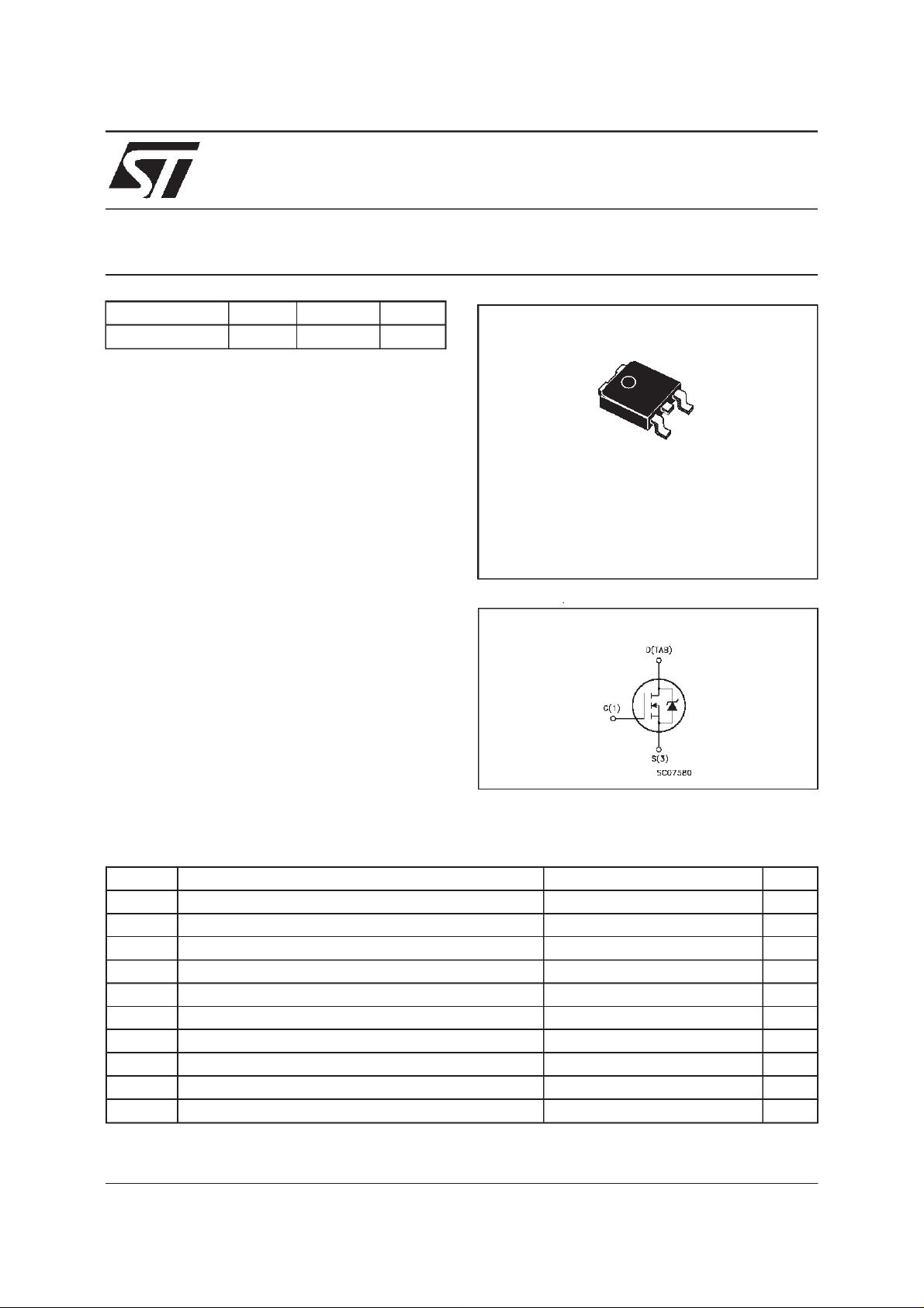
DPAK
TO-252
(Suffix ”T4”)
ADD SUFFIX ”T4”FOR ORDERING IN TAPE & REEL
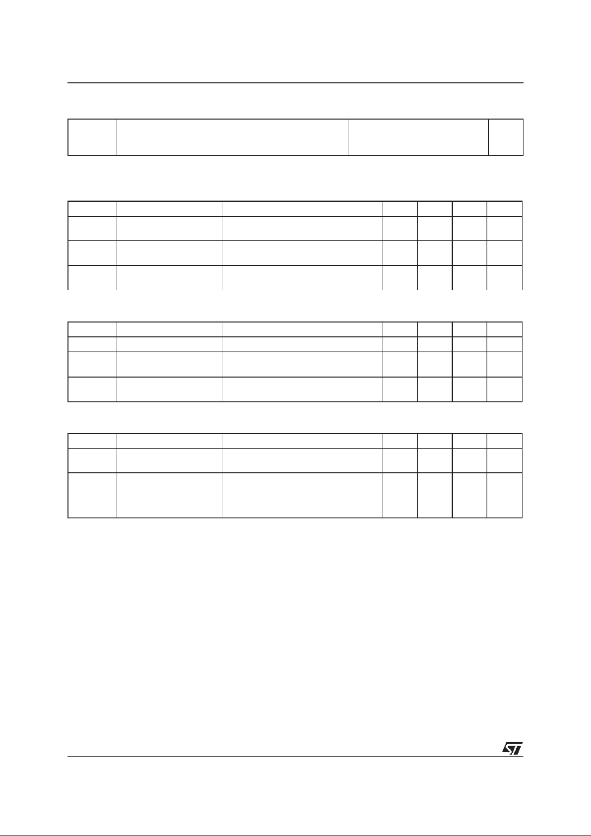
INTERNAL SCHEMATIC DIAGRAM
APPLICATIONS
■ SPECIFICALLYDESIGNEDAND
OPTIMISEDFOR HIGH EFFICIENCYCPU
CORE DC/DC CONVERTERS
ABSOLUTE MAXIMUM RATINGS
Symbol Parameter Value Unit
V
V
V
I
D
I
D
I
DM
P
T
(•) Current Limited By The Package
(••) Pulse widthlimited by safe operatingarea
Dra in- sour c e Volt age (VGS=0) 20 V
DS
Dra in- gate Vol tage (RGS=20kΩ)20V
DGR
Gat e-source V oltage
GS
(•) Dra in Current (continuous) at Tc=25oC20A
(•)Dra in Current (continuous) at Tc=100oC20A
(••) Dra in Current (p uls ed ) 80 A
Tot al Dis s ipation at Tc=25oC55W
tot
Der ati ng Fac t or 0.37 W/
St orage Tempe r at ur e -65 to 175
stg
T
Max. Operating Junction Temperature 175
j
20 V
±
o
C
o
C
o
C
20/01/2000
1/6
Page 2
STD40NF02L
THERMAL DATA
R
thj-case
R
thj-amb
T
Ther mal Resistanc e Junct ion-case Max
Ther mal Resistanc e Junct ion-ambient Max
Maximum Lead T e m pe ra t ure For Soldering P urpose
l
2.73
62.5
300
o
C/W
o
C/W
o
C
ELECTRICAL CHARACTERISTICS
=25oC unless otherwisespecified)
(T
case
OFF
Symbol Parameter Test Con ditions Min. Typ. M ax. Unit
V
(BR)DSS
Drain-source
ID=250µAVGS=0 20 V
Break dow n Voltage
I
DSS
I
GSS
Zero Gate Voltage
Drain Current ( V
GS
Gat e- bod y Leakage
Current (V
DS
=0)
=0)
V
=MaxRating
DS
=MaxRating Tc=125oC
V
DS
V
= ± 20 V ± 100 nA
GS
1
10
ON(∗)
Symbol Parameter Test Con ditions Min. Typ. Max. Unit
V
GS(th)
R
DS(on)
I
D(on)
Gate Threshold Voltage VDS=VGSID= 250 µA12.5V
Sta t ic Drain-sourc e On
Resistance
On State Drain Current VDS>I
VGS=10V ID=20A
V
=5V ID=20A
GS
D(on)xRDS(on)max
0.01
0.015
0.013
0.019
20 A
VGS=10V
DYNAMIC
Symbol Parameter Test Con ditions Min. Typ. Max. Unit
g
(∗)Forward
fs
Tr ansc on duc tance
C
C
C
Input Capacitance
iss
Out put Capacitanc e
oss
Reverse Transfer
rss
Capacit a nc e
VDS>I
D(on)xRDS(on)maxID
=20 A 40 S
VDS=25V f=1MHz VGS= 0 1500
900
200
µA
µ
Ω
Ω
pF
pF
pF
A
2/6
Page 3

STD40NF02L
ELECTRICAL CHARACTERISTICS
(continued)
SWITCHINGON
Symbol Parameter Test Con ditions Min. Typ. Max. Unit
t
d(on)
t
Tur n-on Delay Time
Rise T i m e
r
VDD=15V ID=20A
R
=4.7
G
Ω
VGS=4.5V
20
170
(Resis t iv e Load, see fig. 3)
Q
Q
Q
Tot al Gate C harge
g
Gat e- Source Charg e
gs
Gate-Drain Charge
gd
VDD=16V ID=20A VGS=10V 36
5
10
45 nC
SWITCHINGOFF
Symbol Parameter Test Con ditions Min. Typ. Max. Unit
t
d(off)
Tur n-of f Delay Time
t
Fall Time
f
VDD=15V ID=20A
R
=4.7
G
Ω
VGS=4.5V
40
60
(Resis t iv e Load, see fig. 3)
SOURCEDRAIN DIODE
Symbol Parameter Test Con ditions Min. Typ. Max. Unit
I
V
I
SDM
SD
Q
I
RRM
SD
t
Source-drain Current
(•)
Source-drain Current
20
80
(pulsed)
(∗)ForwardOnVoltage ISD=20 A VGS=0 1.2 V
Reverse Recovery
rr
Time
Reverse Recovery
rr
ISD= 20 A di/dt = 100 A/µs
=15V Tj=150oC
V
DD
(see test circuit, fig. 5)
T.B.D ns
Charge
Reverse Recovery
Current
ns
ns
nC
nC
ns
ns
A
A
µ
A
C
(∗) Pulsed: Pulse duration = 300µs, dutycycle 1.5 %
(•) Pulsewidth limitedby safe operating area
3/6
Page 4

STD40NF02L
Fig. 1:
UnclampedInductive Load Test Circuit
Fig. 3: SwitchingTimes Test CircuitsFor
ResistiveLoad
Fig. 2:
UnclampedInductiveWaveform
Fig. 4: Gate Chargetest Circuit
Fig. 5:
Test CircuitFor InductiveLoad Switching
And DiodeRecovery Times
4/6
Page 5

TO-252 (DPAK) MECHANICAL DATA
STD40NF02L
DIM.
mm inch
MIN. TYP. MAX. MIN. TYP. MAX.
A 2.2 2.4 0.086 0.094
A1 0.9 1.1 0.035 0.043
A2 0.03 0.23 0.001 0.009
B 0.64 0.9 0.025 0.035
B2 5.2 5.4 0.204 0.212
C 0.45 0.6 0.017 0.023
C2 0.48 0.6 0.019 0.023
D 6 6.2 0.236 0.244
E 6.4 6.6 0.252 0.260
G 4.4 4.6 0.173 0.181
H 9.35 10.1 0.368 0.397
L2 0.8 0.031
L4 0.6 1 0.023 0.039
H
A
E
C2
L2
B2
==
==
DETAIL”A”
D
2
13
L4
A1
C
A2
DETAIL”A”
B
G
==
0068772-B
5/6
Page 6

STD40NF02L
Information furnishedis believed tobe accurate and reliable.However, STMicroelectronics assumes no responsibility forthe consequences
of use of such information nor for any infringement of patents or other rights of third parties which may result from its use. No license is
granted by implication orotherwise under anypatentor patent rights of STMicroelectronics. Specificationmentioned in this publicationare
subjecttochange without notice. This publication supersedes and replaces all informationpreviouslysupplied.STMicroelectronicsproducts
are not authorized for useas criticalcomponentsin life support devicesor systemswithout expresswritten approvalof STMicroelectronics.
The ST logo is a trademark ofSTMicroelectronics
1999 STMicroelectronics – Printed in Italy – All Rights Reserved
STMicroelectronics GROUP OF COMPANIES
Australia - Brazil - China- Finland - France - Germany - Hong Kong - India - Italy - Japan - Malaysia - Malta - Morocco -
6/6
Singapore - Spain - Sweden - Switzerland - United Kingdom - U.S.A.
http://www.st.com
.
 Loading...