

Page 1
STD3NC60
STD3NC60-1
N-CHANNEL 600V - 1.8Ω - 3.2A DPAK / IPAK
PowerMesh™II MOSFET
TYPE V
STD3NC60
STD3NC60-1
■ TYPICAL R
■ EXTREMELY HIGHdv/dt CAPABILITY
■ 100% AVALANCHE TESTED
■ NEW HIGH VOLTAGE BENCHMARK
■ GATE CHARGE MINIMIZED
■ ADD SUFFIX “T4” FOR ORDERING IN TAPE &
DS
DSS
600V
600V
(on) = 1.8Ω
R
DS(on)
<2.2Ω
<2.2Ω
I
D
3.2A
3.2A
REEL (SMD PACKAGE)
DESCRIPTION
The PowerMESH
generation of MESH OVERLAY
™II is the evolution of the first
™. T he layout re-
finements introduced greatly improv e the Ron*area
figure of m erit while keeping the device at the leading edge for what con cerns swithing s peed, gate
charge and ruggedness.
APPLICATIONS
■ HIGH CURRENT, HIGH SPEED SWITCHING
■ SWITH MODE POWER SUPPLIES (SMPS)
■ DC-AC CONVERTERS FOR WELDING
EQUIPMENT AND UNINTERRUPTIBLE
POWER SUPPLIES AND MOTOR DRIVERS
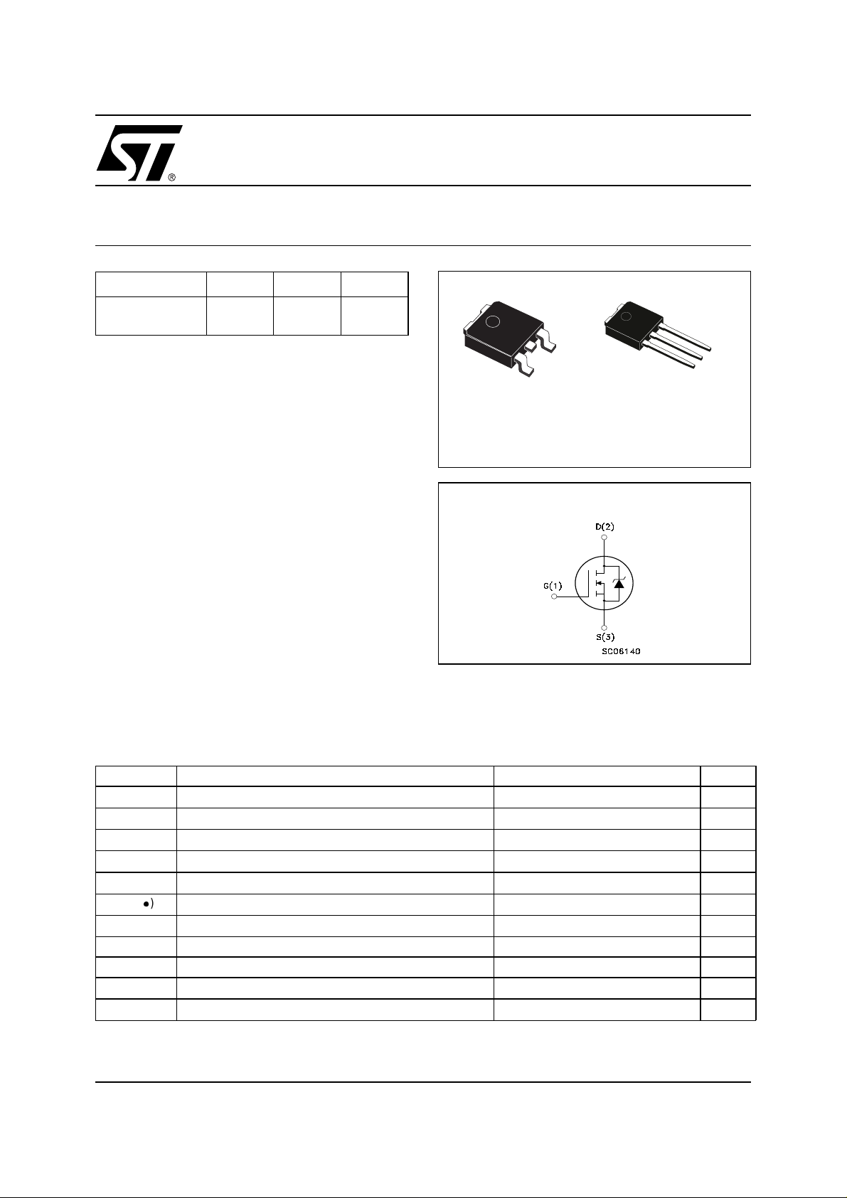
3
1
DPAK IPAK
No Suffix
(Suffix”-1”)
INTERNAL SCHEMATIC DIAGRAM
3
2
1
ABSOLUTE MAXIMUM RATINGS
Symbol Parameter Value Unit
V
DS
V
DGR
V
GS
I
D
I
D
I
DM
P
TOT
dv/dt(1) Peak Diode Recovery voltage slope 3.5 V/ns
T
stg
T
(•)Pulse width limited by safe operating area
≤3.2A, di/dt ≤300A/µs, VDD≤ V
(1)I
SD
Drain-source Voltage (VGS=0)
Drain-gate Voltage (RGS=20kΩ)
600 V
600 V
Gate- source Voltage ±30 V
Drain Current (continuos) at TC= 25°C
Drain Current (continuos) at TC= 100°C
()
Drain Current (pulsed) 12.8 A
Total Dissipation at TC= 25°C
3.2 A
2A
50 W
Derating Factor 0.4 W/°C
Storage Temperature –65 to 150 °C
Max. Operating Junction Temperature 150 °C
j
(BR)DSS,Tj≤TJMAX.
1/10August 2002
Page 2

STD3NC60 - STD3NC60-1
THERMAL DATA
Rthj-case Thermal Resistance Junction-case Max 2.5 °C/W
Rthj-amb Thermal Resistance Junction-ambient Max 100 °C/W
T
AVALANCHE CHARACTERISTICS
Symbol Parameter Max Value Unit
I
AR
E
AS
ELECTRICAL CHARACTERISTICS (TCASE = 25 °C UNLESS OTHERWISE SPECIFIED)
OFF
Symbol Parameter Test Conditions Min. Typ. Max. Unit
V
(BR)DSS
I
DSS
I
GSS
Maximum Lead Temperature For Soldering Purpose 275 °C
l
Avalanche Current, Repetitive or Not-Repetitive
(pulse width limited by T
max)
j
Single Pulse Avalanche Energy
(starting T
Drain-source
= 25 °C, ID=IAR,VDD=50V)
j
ID= 250 µA, VGS= 0 600 V
3.2 A
270 mJ
Breakdown Voltage
Zero Gate Voltage
Drain Current (V
GS
Gate-body Leakage
Current (V
DS
=0)
=0)
V
= Max Rating
DS
= Max Rating, TC= 125 °C
V
DS
V
= ±30V ±100 nA
GS
1µA
50 µA
ON (1)
Symbol Parameter Test Conditions Min. Typ. Max. Unit
V
GS(th)
R
DS(on)
Gate Threshold Voltage
Static Drain-source On
V
DS=VGS,ID
VGS=10V,ID= 1.5 A
= 250µA
234V
1.8 2.2 Ω
Resistance
DYNAMIC
Symbol Parameter Test Conditions Min. Typ. Max. Unit
(1) Forward Transconductance VDS>I
g
fs
C
iss
C
oss
C
rss
Input Capacitance
Output Capacitance 72 pF
Reverse Transfer
Capacitance
D(on)xRDS(on)max,
ID=2A
V
=25V,f=1MHz,VGS=0
DS
3.7 S
475 pF
10 pF
2/10
Page 3
STD3NC60 - STD3N C60-1
ELECTRICAL CHARACTERISTICS (CONTINUED)
SWITCHING ON
Symbol Parameter Test Conditions Min. Typ. Max. Unit
V
t
d(on)
Q
Q
Q
t
r
gs
gd
Turn-on Delay Time
Rise Time 14 ns
Total Gate Charge
g
Gate-Source Charge 2.5 nC
Gate-Drain Charge 9 nC
SWITCHING OFF
Symbol Parameter Test Conditions Min. Typ. Max. Unit
t
r(Voff)
t
t
f
c
Off-voltage Rise Time
Fall Time 19 ns
Cross-over Time 24 ns
SOURCE DRAIN DIODE
Symbol Parameter Test Conditions Min. Typ. Max. Unit
I
SD
I
SDM
VSD(1)
t
rr
Q
rr
I
RRM
Note: 1. Pulsed: Pulse duration = 300 µs, duty cycle 1.5 %.
2. Pulse width limited by safe operating area.
Source-drain Current 3.2 A
(2)
Source-drain Current (pulsed) 12.8 A
Forward On Voltage
Reverse Recovery Time
Reverse Recovery Charge 2.7 µC
Reverse Recovery Current 9 A
= 300V, ID=2A
DD
R
= 4.7Ω VGS=10V
G
(see test circuit, Figure 3)
V
= 480V, ID=4A,
DD
=10V
V
GS
V
=480V,ID=4A,
DD
RG= 4.7Ω, VGS=10V
(see test circuit, Figure 5)
ISD= 3.2A, VGS=0
I
= 4A, di/dt = 100A/µs,
SD
= 100V, Tj= 150°C
V
DD
(see test circuit, Figure 5)
14 ns
16.5 23.1 nC
15 ns
1.6 V
600 ns
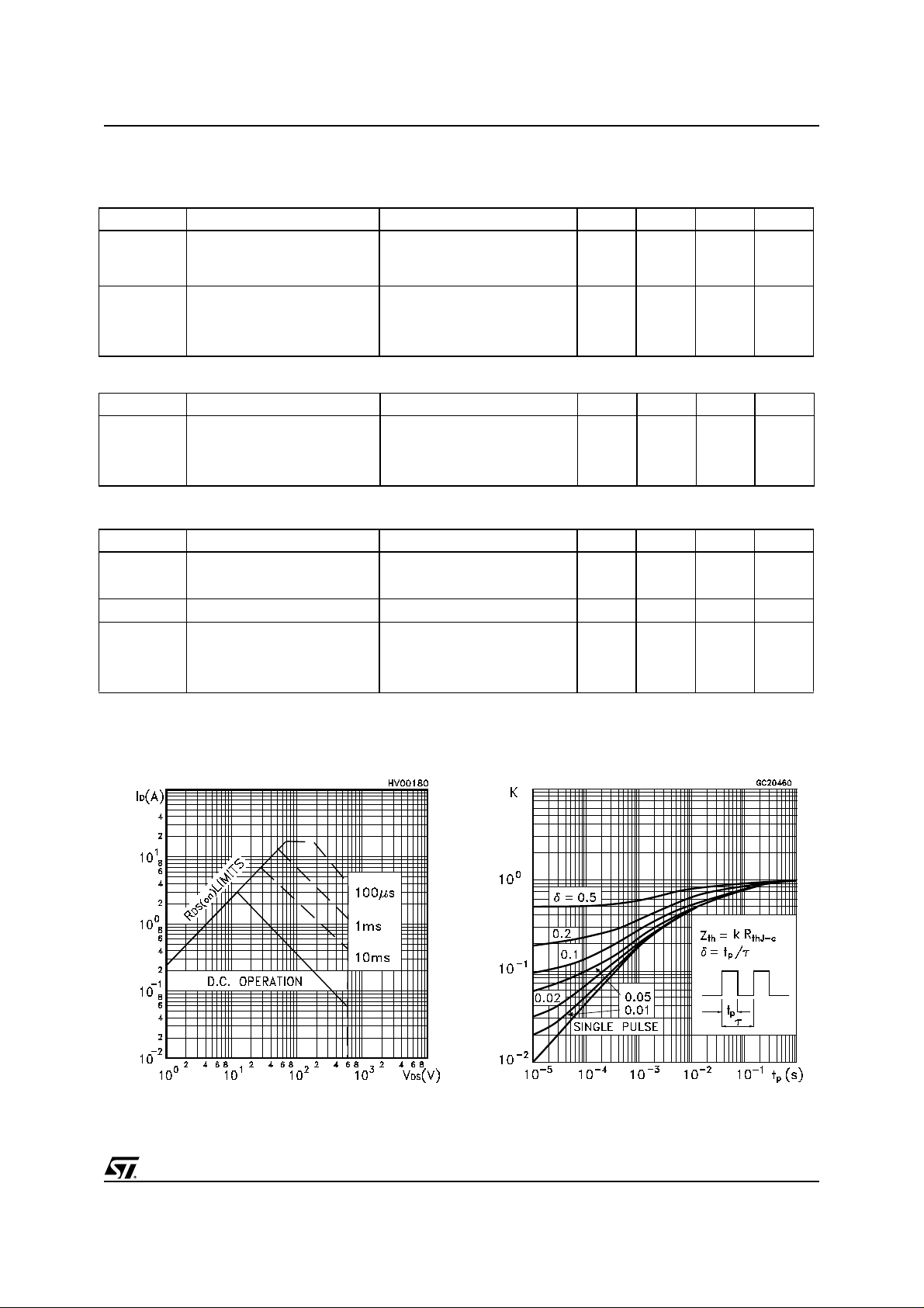
Safe Operating Area
Thermal Impedance
3/10
Page 4

STD3NC60 - STD3NC60-1
Output Characteristics Tranfer Characteristics
Tranconductance
Static Drain-Source On Resistance
Capacitance VariationsGate Charge vs Gate-so urce Voltage
4/10
Page 5

Source-drain Diode Forward Characteristics
STD3NC60 - STD3N C60-1
Normalized On Resistance vs TemperatureNormalized Gate Theresho ld Voltage vs Temp.
5/10
Page 6

STD3NC60 - STD3NC60-1
Fig. 2: Unclamped Inductive WaveformFig. 1: Unclamped Inductive Load Test Circuit
Fig. 3: Switching Times Test Circuits For
Resistive Loa d
Fig. 5: Test Circuit For Inductive Load Switching
And Diode Recovery Times
Fig. 4: Gate Charge test Circuit
6/10
Page 7

TO-251 (IPAK) MECHANI CAL DAT A
STD3NC60 - STD3N C60-1
DIM.
MIN. TYP. MAX. MIN. TYP. MAX.
mm inch
A 2.2 2.4 0.086 0.094
A1 0.9 1.1 0.035 0.043
A3 0.7 1.3 0.027 0.051
B 0.64 0.9 0.025 0.031
B2 5.2 5.4 0.204 0.212
B3 0.85 0.033
B5 0.3 0.012
B6 0.95 0.037
C 0.45 0.6 0.017 0.023
C2 0.48 0.6 0.019 0.023
D 6 6.2 0.236 0.244
E 6.4 6.6 0.252 0.260
G 4.4 4.6 0.173 0.181
H 15.9 16.3 0.626 0.641
L 9 9.4 0.354 0.370
L1 0.8 1.2 0.031 0.047
L2 0.8 1 0.031 0.039
H
A
C2
L2
E
B2
= =
= =
D
B3
2
1 3
L1
A1
L
B6
C
A3
B
B5
G
= =
0068771-E
7/10
Page 8

STD3NC60 - STD3NC60-1
TO-252 (DPAK) MECHANICAL DATA
DIM.
A 2.20 2.40 0.087 0.094
A1 0.90 1.10 0.035 0.043
A2 0.03 0.23 0.001 0.009
B 0.64 0.90 0.025 0.035
B2 5.20 5.40 0.204 0.213
C 0.45 0.60 0.018 0.024
C2 0.48 0.60 0.019 0.024
D 6.00 6.20 0.236 0.244
E 6.40 6.60 0.252 0.260
G 4.40 4.60 0.173 0.181
H 9.35 10.10 0.368 0.398
L2 0.8 0.031
L4 0.60 1.00 0.024 0.039
V2 0
MIN. TYP. MAX. MIN. TYP. MAX.
o
mm inch
o
8
o
0
o
0
8/10
P032P_B
Page 9

STD3NC60 - STD3N C60-1
DPAK FOOTPRINT
All dimensions are i n millimeters
TAPE AND REEL SHIPMENT (suffix ”T4”)*
TUBE SHIPMENT (no suffix)*
All dimensions
are in millimeters
REEL MECHANICAL DATA
DIM.
A 330 12.992
B 1.5 0.059
C 12.8 13.2 0.504 0.520
D 20.2 0.795
G 16.4 18.4 0.645 0.724
N 50 1.968
T 22.4 0.881
mm inch
MIN. MAX. MIN. MAX.
TAPE MECHANICAL DATA
DIM.
A0 6.8 7 0.267 0.275
B0 10.4 10.6 0.409 0.417
B1 12.1 0.476
D 1.5 1.6 0.059 0.063
D1 1.5 0.059
E 1.65 1.85 0.065 0.073
F 7. 4 7.6 0.291 0.299
K0 2.55 2.75 0.100 0.108
P0 3.9 4.1 0.153 0.161
P1 7.9 8.1 0.311 0.319
P2 1.9 2.1 0.075 0.082
R 40 1.574
W 15.7 16.3 0.618 0.641
* on sales ty pe
mm inch
MIN. MAX. MIN. MAX.
BASE QTY BULK QTY
2500 2500
9/10
Page 10

STD3NC60 - STD3NC60-1
Information furnished is believed to be accurate and reliable. However, STMicroelectronics assumes no responsibility f or t he
consequences of use of su ch in formation nor for any in fringement of patents or other rights of third parties w hich may result from
its use. No license is granted by implication or otherwise under any patent or patent rights of STMicroelectronics. Specifications
mentioned in this publication are subject to change without notice. This publication supersedes and replaces all information
previously suppli ed. STMi croelect ronics pr oducts are not author ized for use as cr itical component s in li fe suppo rt devi ces or
systems without express written approval of STMicroelectronics.
Australia - Brazil - Canada - China - Finland - France - Germany - Hong Kong - India - Israel - Italy - Japan - Malaysia - Malta - Morocco
© The ST logo is a registered trademark of STMicroelectronics
© 2002 STMicroelectronics - Printed in Italy - All Rights Reserved
Singapore - Spain - Sweden - Switzerland - United Kingdom - United States.
STMicroelectronics GROUP OF COMPANIES
© http://www.st.com
10/10
 Loading...