

Page 1
N - CHANNEL 600V - 2 Ω - 3.2A TO-251/TO-252
TYPE V
ST D3 NC6 0 600 V < 2.2 Ω 3.2 A
ν TYPICALR
ν EXTREMELYHIGHdv/dtCAPABILITY
ν 100% AVALANCHETESTED
ν NEWHIGH VOLTAGE BENCHMARK
ν GATECHARGE MINIMIZED
DS(on)
DSS
=2Ω
DESCRIPTION
The PowerMESH is the evolution of the first
generation of MESH OVERLAY. The layout
refinements introduced greatly improve the
Ron*area figure of merit while keepingthe device
at the leading edge for what concerns switching
speed, gate chargeand ruggedness.
APPLICATIONS
ν HIGH CURRENT, HIGH SPEEDSWITCHING
ν SWITHMODE POWERSUPPLIES (SMPS)
ν DC-AC CONVERTERSFORWELDING
EQUIPMENTANDUNINTERRUPTIBLE
POWERSUPPLIESAND MOTORDRIVER
R
DS(on)
I
D
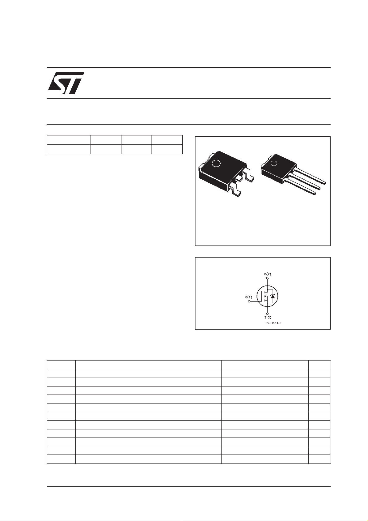
STD3NC60
PowerMESH MOSFET
PRELIMINARY DATA
3
1
DPAK
TO-252
(Suffix ”T4”)
INTERNAL SCHEMATIC DIAGRAM
IPAK
TO-251
(Suffix”-1”)
2
1
3
ABSOLUTE MAXIMUM RATINGS
Symbol Parameter Value Uni t
V
V
V
I
DM
P
dv/dt(
T
February 2000
Drain-source Vol t age (VGS= 0) 600 V
DS
Drain- gat e Voltage (RGS=20kΩ)
DGR
Gate-s ource Voltage ± 30 V
GS
Drain Curr ent (cont in uous ) at Tc=25oC 3.2 A
I
D
Drain Curr ent (cont in uous ) at Tc= 100oC2A
I
D
(•) Drain Current (pulsed) 12.8 A
Tot al Diss ipat i on at Tc=25oC50W
tot
Derating Factor 0.4 W/
1) Peak Diode Rec overy voltage slope 3 V/ns
St orage Te mper ature -65 to 150
stg
Max. Operating Ju nction T emperature 150
T
j
600 V
o
C
o
C
o
C
1/8
Page 2
STD3NC60
THERMAL DATA
R
thj-cas e
Rthj-amb
R
thc-sin k
T
AVALANCHE CHARACTERISTICS
Symb ol Parameter Max Val ue Uni t
I
AR
E
Therma l Resistan ce Juncti on-c as e Max
Therma l Resistan ce Juncti on-am b ien t Max
Therma l Resistan ce Case-sink Typ
Maxim um Lead Temperature For Sol dering P urpose
l
Avalanc h e Cur rent , Repetit ive or N ot-Repet it ive
(pulse width li mit ed by T
Single Puls e A valanche Energy
AS
(starting T
=25oC, ID=IAR,VDD=50V)
j
max)
j
2.5
100
1.5
275
3.2 A
220 mJ
o
C/W
oC/W
o
C/W
o
C
ELECTRICAL CHARACTERISTICS (T
=25oC unlessotherwisespecified)
case
OFF
Symb ol Parameter Test Conditions Mi n . Typ . Max. Unit
V
(BR) DSS
Drain-s ource
= 250 µ AVGS=0
I
D
600 V
Break down Voltage
I
DSS
I
GSS
Zero Gate Voltage
Drain Curre nt (V
GS
Gate-body Leak a ge
Current (V
DS
=0)
=0)
V
=MaxRating
DS
= Max Rating Tc= 125oC
V
DS
= ± 30 V
V
GS
1
50
± 100 nA
ON (∗)
Symb ol Parameter Test Conditions Mi n . Typ . Max. Unit
V
GS(th)
R
DS(on)
Gate Threshold Voltage
Static Drain- s ource O n
V
DS=VGSID
=250µA
VGS= 10V ID=1.5A 2 2.2 Ω
234V
Resistance
I
D(on)
On State Drain Current VDS>I
D(on)xRDS(on)max
3.2 A
VGS=10V
DYNAMIC
Symb ol Parameter Test Conditions Mi n . Typ . Max. Unit
g
(∗)Forward
fs
Transconductanc e
Input Capacit anc e
iss
Output Capacitance
Reverse Transfer
rss
C
C
oss
C
Capacit ance
VDS>I
D(on)xRDS(on)maxID
=1.5A 2 S
VDS=25V f=1MHz VGS= 0 700
85
9
µA
µA
pF
pF
pF
2/8
Page 3
STD3NC60
ELECTRICAL CHARACTERISTICS (continued)
SWITCHING ON
Symb ol Parameter Test Conditions Mi n . Typ . Max. Unit
t
d(on)
t
r
Turn-on T ime
Rise Time
VDD=300V ID=1.5A
=4.7 Ω VGS=10V
R
G
(see test circuit, figure 3)
Q
Q
Q
Total Gate Charge
g
Gate-Source Charge
gs
Gate-Drain Charge
gd
VDD=480V ID=3.2A VGS=10V 18
SWITCHING OFF
Symb ol Parameter Test Conditions Mi n . Typ . Max. Unit
t
r(Voff)
t
t
Off -voltag e Rise Time
Fall T ime
f
Cross -over Time
c
VDD=480V ID=3.2A
=4.7 Ω VGS=10V
R
G
(see test circuit, figure 5)
SOURCEDRAINDIODE
Symb ol Parameter Test Conditions Mi n . Typ . Max. Unit
I
SD
I
SDM
V
SD
t
Q
I
RRM
(∗) Pulsed: Pulse duration = 300µs, dutycycle 1.5 %
(•) Pulse width limitedby safe operatingarea
Source-drain Current
(•)
Source-drain Current
(pulsed)
(∗)ForwardOnVoltage ISD=3.2A VGS=0 1.6 V
Revers e Recover y
rr
Time
Revers e Recover y
rr
=3.2A di/dt=100A/µs
I
SD
=100V Tj= 150oC
V
DD
(see test circuit, figure 5)
Charge
Revers e Recover y
Current
14
11
25 nC
6
8
10
8
7
3.2
12.8
610
3.6
11.7
ns
ns
nC
nC
ns
ns
ns
A
A
ns
µC
A
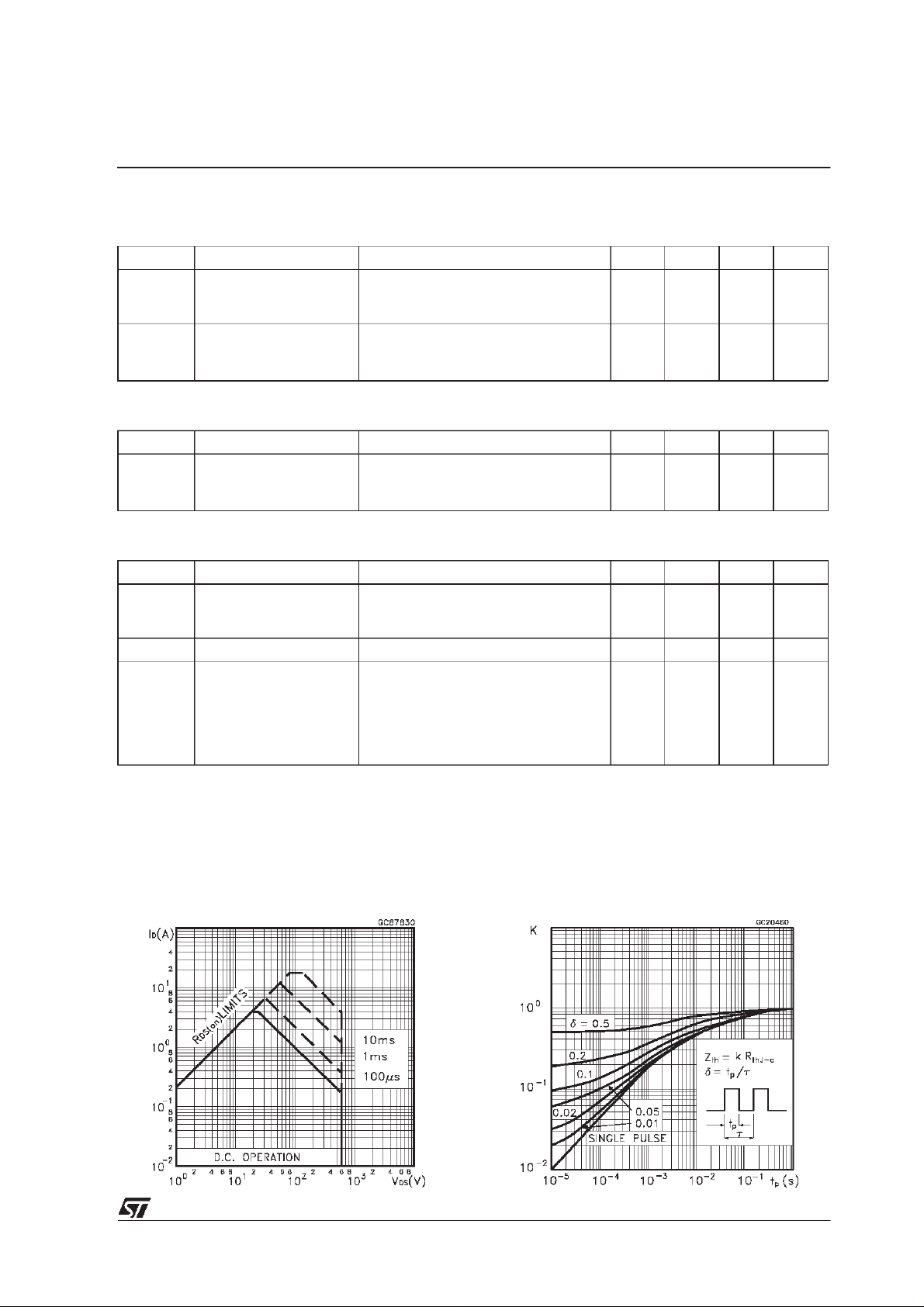
Safe Operating Area Thermal Impedance
3/8
Page 4

STD3NC60
OutputCharacteristics
Transconductance
TransferCharacteristics
StaticDrain-source On Resistance
Gate Chargevs Gate-sourceVoltage
4/8
CapacitanceVariations
Page 5

STD3NC60
NormalizedGate ThresholdVoltagevs
Temperature
Source-drainDiode Forward Characteristics
Normalized OnResistance vs Temperature
5/8
Page 6

STD3NC60
Fig. 1: UnclampedInductive Load TestCircuit
Fig. 3: SwitchingTimes TestCircuitsFor
ResistiveLoad
Fig. 2: UnclampedInductiveWaveform
Fig. 4: GateChargetest Circuit
Fig. 5: Test Circuit For InductiveLoadSwitching
And DiodeRecoveryTimes
6/8
Page 7

TO-251 (IPAK) MECHANICAL DATA
STD3NC60
DIM.
MIN. TYP. MAX. MIN. TYP. MAX.
mm inch
A 2.2 2.4 0.086 0.094
A1 0.9 1.1 0.035 0.043
A3 0.7 1.3 0.027 0.051
B 0.64 0.9 0.025 0.031
B2 5.2 5.4 0.204 0.212
B3 0.85 0.033
B5 0.3 0.012
B6 0.95 0.037
C 0.45 0.6 0.017 0.023
C2 0.48 0.6 0.019 0.023
D 6 6.2 0.236 0.244
E 6.4 6.6 0.252 0.260
G 4.4 4.6 0.173 0.181
H 15.9 16.3 0.626 0.641
L 9 9.4 0.354 0.370
L1 0.8 1.2 0.031 0.047
L2 0.8 1 0.031 0.039
H
A
E
==
C2
L2
B2
==
D
B3
2
13
L1
B6
A1
C
A3
L
B
B5
G
==
0068771-E
7/8
Page 8

STD3NC60
TO-252 (DPAK) MECHANICAL DATA
DIM.
mm inch
MIN. TYP. MAX. MIN. TYP. MAX.
A 2.2 2.4 0.086 0.094
A1 0.9 1.1 0.035 0.043
A2 0.03 0.23 0.001 0.009
B 0.64 0.9 0.025 0.035
B2 5.2 5.4 0.204 0.212
C 0.45 0.6 0.017 0.023
C2 0.48 0.6 0.019 0.023
D 6 6.2 0.236 0.244
E 6.4 6.6 0.252 0.260
G 4.4 4.6 0.173 0.181
H 9.35 10.1 0.368 0.397
L2 0.8 0.031
L4 0.6 1 0.023 0.039
8/8
H
A
E
==
C2
L2
B2
==
DETAIL”A”
D
2
13
L4
A1
C
A2
DETAIL”A”
B
G
==
0068772-B
Page 9

STD3NC60
Information furnished is believed to be accurate and reliable. However, STMicroelectronics assumes noresponsibility for the consequences
of use of such information nor for any infringement of patents or other rights of third parties which may result from its use. No license is
granted by implication or otherwise under any patent or patent rights of STMicroelectronics. Specification mentioned in this publication are
subject to change withoutnotice. Thispublication supersedes and replaces allinformation previously supplied. STMicroelectronics products
are not authorized for use as critical components in life support devices or systems without express written approval ofSTMicroelectronics.
The ST logo is a trademarkof STMicroelectronics
2000 STMicroelectronics – Printed in Italy – All Rights Reserved
STMicroelectronics GROUP OF COMPANIES
Australia - Brazil -China - Finland- France- Germany -Hong Kong - India- Italy- Japan - Malaysia- Malta -Morocco -
Singapore - Spain - Sweden -Switzerland - United Kingdom- U.S.A.
http://www.st.com
9/8
 Loading...