

Page 1
N - CHANNEL 500V - 2.4Ω - 3A TO-251/TO-252
TYPE V
DSS
ST D3N C50 50 0 V < 2.7 Ω 3A
■ TYPICALR
■ EXTREMELYHIGH dv/dt CAPABILITY
■ 100%AVALANCHETESTED
■ NEWHIGH VOLTAGE BENCHMARK
■ GATECHARGE MINIMIZED
■ ADDSUFFIX ”T4” FORORDERING INTAPE
DS(on)
= 2.4 Ω
& REEL.
R
DS(on)
I
D
STD3NC50
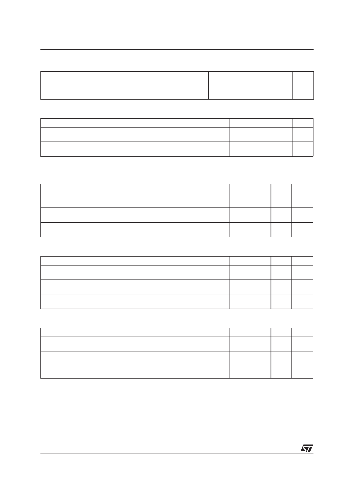
PowerMESH ΙΙ MOSFET
PRELIMINARY DATA
3
1
2
1
3
DESCRIPTION
The PowerMESH
is the evolution of the first
ΙΙ
generation of MESH OVERLAY. The layout
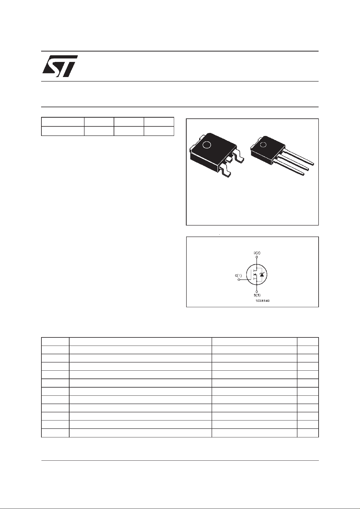
DPAK
TO-252
(Suffix ”T4”)
IPAK
TO-251
(Suffix”-1”)
refinements introduced greatly improve the
Ron*areafigure of meritwhile keeping the device
at the leading edge for what concerns switching
speed,gate chargeand ruggedness.
INTERNAL SCHEMATIC DIAGRAM
APPLICATIONS
■ HIGHCURRENT, HIGH SPEEDSWITCHING
■ SWITHMODE POWER SUPPLIES (SMPS)
■ DC-AC CONVERTERS FOR WELDING
EQUIPMENTAND UNINTERRUPTIBLE
POWERSUPPLIESAND MOTORDRIVER
ABSOLUTE MAXIMUM RATINGS
Symbol Parameter Value Unit
V
V
V
I
DM
P
dv/ dt(
T
(•) Pulse width limited by safe operating area (1)ISD≤3 A, di/dt ≤ 100 A/µs, VDD≤ V
Drain-source Voltage (VGS=0) 500 V
DS
Dra in- gate Voltage (RGS=20kΩ)
DGR
Gate -sourc e Voltage
GS
Drain Current (continuous) at Tc=25oC3.2A
I
D
Drain Current (continuous) at Tc=100oC2A
I
D
500 V
30 V
±
(•) Drain Current (pulsed) 12.8 A
Total Dissipation at Tc=25oC60W
tot
Derating Factor 0.48 W/
1) P eak Dio de Recovery volt age slope 4 V/ns
St orage Tempe rature -65 to 150
stg
Max. Op erating Junc t ion T e m pe rat ure 150
T
j
,Tj≤T
(BR)DSS
JMAX
o
C
o
C
o
C
January 2000
1/7
Page 2
STD3NC50
THERMAL DATA
R
thj-case
Rthj-amb
R
thc-sink
T
AVALANCHE CHARACTERISTICS
Symbol Para meter Max Val ue Uni t
I
AR
E
Ther mal Resist an c e J unction- case Max
Ther mal Resist an c e J unction- ambient Max
Thermal Resistance Case-sink Typ
Maximum Lead Tem perature Fo r Soldering P urpose
l
Avalanche Curr ent, Repetit ive or Not-Re petitive
(pulse width limited by T
Single Pu lse Avalanche Energy
AS
(starting T
=25oC, ID=IAR,VDD=50V)
j
max)
j
2.0
100
1.5
275
3A
40 mJ
o
C/W
oC/W
o
C/W
o
C
ELECTRICAL CHARACTERISTICS (T
=25oC unless otherwisespecified)
case
OFF
Symbol Parameter Test Conditions Min. Typ. Max. Unit
V
(BR)DSS
Drain-source
=250µAVGS=0
I
D
500 V
Break d own V o lt age
I
DSS
I
GSS
Zero Gate Voltage
Drain Cu rr ent (V
GS
Gat e- b ody Le akage
Current (V
DS
=0)
=0)
V
=MaxRating
DS
= Max Rating Tc=125oC
V
DS
= ± 30 V
V
GS
1
50
± 100 nA
ON(∗)
Symbol Parameter Test Conditions Min. Typ. Max. Unit
V
GS(th)
Gate Threshold
V
DS=VGSID
= 250 µA
234V
Voltage
R
DS(on)
Static Drain-source On
VGS=10V ID= 1.5 A 2.4 2.7
Resistance
I
D(on)
On Stat e D ra in Curr ent VDS>I
D(on)xRDS(on)max
3A
VGS=10V
DYNAMIC
Symbol Parameter Test Conditions Min. Typ. Max. Unit
g
(∗)Forward
fs
Tr ansconductance
C
C
C
Input Cap ac i t an c e
iss
Out put Capacitanc e
oss
Reverse Transf er
rss
Capacitance
VDS>I
D(on)xRDS(on)maxID
=1.5A 2 S
VDS=25V f=1MHz VGS=0 400
62
7.5
µA
µ
Ω
pF
pF
pF
A
2/7
Page 3
STD3NC50
ELECTRICAL CHARACTERISTICS
(continued)
SWITCHINGON
Symbol Parameter Test Conditions Min. Typ. Max. Unit
t
d(on)
Q
Q
Q
Turn-on Time
t
Rise Time
r
Total Gate Charge
g
Gat e- Source Char ge
gs
Gate-Drain Charge
gd
VDD= 300 V ID=1.5A
R
=4.7
G
Ω
VGS=10V
VDD= 480 V ID=3A VGS=10V 15
11
8
21 nC
6.5
5
SWITCHINGOFF
Symbol Parameter Test Conditions Min. Typ. Max. Unit
t
r(Voff)
t
t
Off -voltage Rise Time
Fall Time
f
Cross-over T i m e
c
VDD= 400 V ID=3A
=4.7 ΩVGS=10V
R
G
8
5
14
SOURCEDRAINDIODE
Symbol Parameter Test Conditions Min. Typ. Max. Unit
I
SD
I
SDM
V
SD
t
Q
I
RRM
(∗) Pulsed: Pulse duration = 300 µs, duty cycle 1.5 %
(•) Pulse width limited by safe operating area
Source-drain Curr ent
(•)
Source-drain Curr ent
3
12
(pulsed)
(∗) For ward On Voltage ISD=3A VGS=0 1.6 V
Reverse Recov ery
rr
Time
Reverse Recov ery
rr
= 3 A d i/ d t = 100 A/µs
I
SD
= 100 V Tj=150oC
V
DD
245
980
Charge
Reverse Recov ery
8
Current
ns
ns
nC
nC
ns
ns
ns
A
A
ns
µ
A
C
3/7
Page 4

STD3NC50
Fig. 1:
UnclampedInductive Load TestCircuit
Fig. 3: SwitchingTimes Test CircuitsFor
ResistiveLoad
Fig. 2:
UnclampedInductiveWaveform
Fig. 4: Gate Chargetest Circuit
Fig. 5:
Test CircuitFor InductiveLoad Switching
And Diode Recovery Times
4/7
Page 5

TO-251(IPAK) MECHANICAL DATA
STD3NC50
DIM.
MIN. TYP. MAX. MIN. TYP. MAX.
mm inch
A 2.2 2.4 0.086 0.094
A1 0.9 1.1 0.035 0.043
A3 0.7 1.3 0.027 0.051
B 0.64 0.9 0.025 0.031
B2 5.2 5.4 0.204 0.212
B3 0.85 0.033
B5 0.3 0.012
B6 0.95 0.037
C 0.45 0.6 0.017 0.023
C2 0.48 0.6 0.019 0.023
D 6 6.2 0.236 0.244
E 6.4 6.6 0.252 0.260
G 4.4 4.6 0.173 0.181
H 15.9 16.3 0.626 0.641
L 9 9.4 0.354 0.370
L1 0.8 1.2 0.031 0.047
L2 0.8 1 0.031 0.039
H
A
E
==
C2
L2
B2
==
D
B3
2
13
L1
B6
A1
C
A3
L
B
B5
G
==
0068771-E
5/7
Page 6

STD3NC50
TO-252 (DPAK) MECHANICAL DATA
DIM.
mm inch
MIN. TYP. MAX. MIN. TYP. MAX.
A 2.2 2.4 0.086 0.094
A1 0.9 1.1 0.035 0.043
A2 0.03 0.23 0.001 0.009
B 0.64 0.9 0.025 0.035
B2 5.2 5.4 0.204 0.212
C 0.45 0.6 0.017 0.023
C2 0.48 0.6 0.019 0.023
D 6 6.2 0.236 0.244
E 6.4 6.6 0.252 0.260
G 4.4 4.6 0.173 0.181
H 9.35 10.1 0.368 0.397
L2 0.8 0.031
L4 0.6 1 0.023 0.039
6/7
H
A
E
C2
L2
B2
==
==
DETAIL”A”
D
2
13
L4
A1
C
A2
DETAIL”A”
B
G
==
0068772-B
Page 7

STD3NC50
Information furnished is believed to be accurate and reliable. However, STMicroelectronics assumes no responsibility for the consequences
of use of such information nor for any infringement of patents or other rights of third parties which may result from its use. No license is
granted by implicationor otherwise under any patent or patent rights of STMicroelectronics. Specification mentioned in this publication are
subject to change without notice. This publication supersedes and replaces all information previously supplied. STMicroelectronics products
are not authorized for use as critical components in life support devices or systems without express written approval of STMicroelectronics.
The ST logo is a trademarkof STMicroelectronics
2000 STMicroelectronics – Printed in Italy – All Rights Reserved
STMicroelectronics GROUP OF COMPANIES
Australia - Brazil -China - Finland - France- Germany - Hong Kong - India - Italy - Japan - Malaysia - Malta - Morocco -
Singapore - Spain - Sweden -Switzerland -United Kingdom - U.S.A.
http://www.st.com
7/7
 Loading...