

Page 1
STD3NB50
3
Obsolete Product(s) - Obsolete Product(s)
STD3NB50-1
N - CHANNEL 500V - 2.5Ω - 3A - IPAK/DPAK
PowerMESH™ MOSFET
PRELIMINARY DATA
Table 1. General Features
Typ e
STD3NB50 500 V < 2.8 Ω 3 A
STD3NB50-1 500 V < 2.8 Ω 3 A
V
DSS
R
DS(on)
I
D
FEATURES SUMMARY
■ TYPICAL R
■ EXTREMELY HIGH dv/dt CAPABILITY
■ 100% AVALANCHE TESTED
■ VERY LOW INTRINSIC CAPACITANCES
■ GATE CHARGE MINIMIZED
DS(on)
= 2.5 Ω
DESCRIPTION
Using the latest high voltage MESH OVERLAY™
process, STMicroelectronics has designed an advanced family of power MOSFETs with outstanding performances. The new patent pending strip
layout coupled with the Company’s proprietary
edge termination structure, gives the lowest
RDS(on) per area, exceptional avalanche and dv/
dt capabilities and unrivalled gate charge and
switching characteristics.
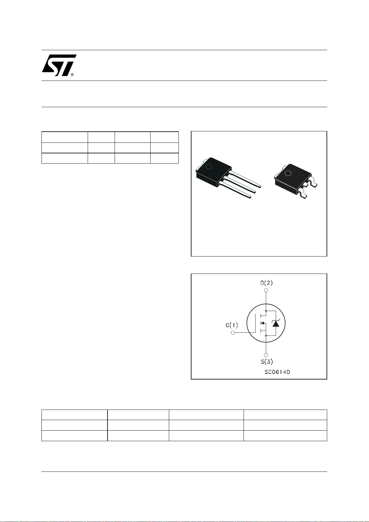
Figure 1. Package
2
1
IPAK
TO-251
DPAK
TO-252
Figure 2. Internal Schematic Diagram
3
1
APPLICATIONS
■ SWITCH MODE POWER SUPPLIES (SMPS)
■ DC-AC CONVERTERS FOR WELDING
EQUIPMENT AND UNINTERRUPTIBLE
POWER SUPPLIES AND MOTOR DRIVE
Table 2. Order Codes
Part Number Marking Package Packaging
STD3NB50T4 D3NB50 DPAK TAPE & REEL
STD3NB50-1 D3NB50 IPAK TUBE
REV. 2
April 2004
This is preliminary information on a new product now in development or undergoing evaluation. Details are subject to change without notice.
1/8
Page 2
Obsolete Product(s) - Obsolete Product(s)
STD3NB50/STD3NB50-1
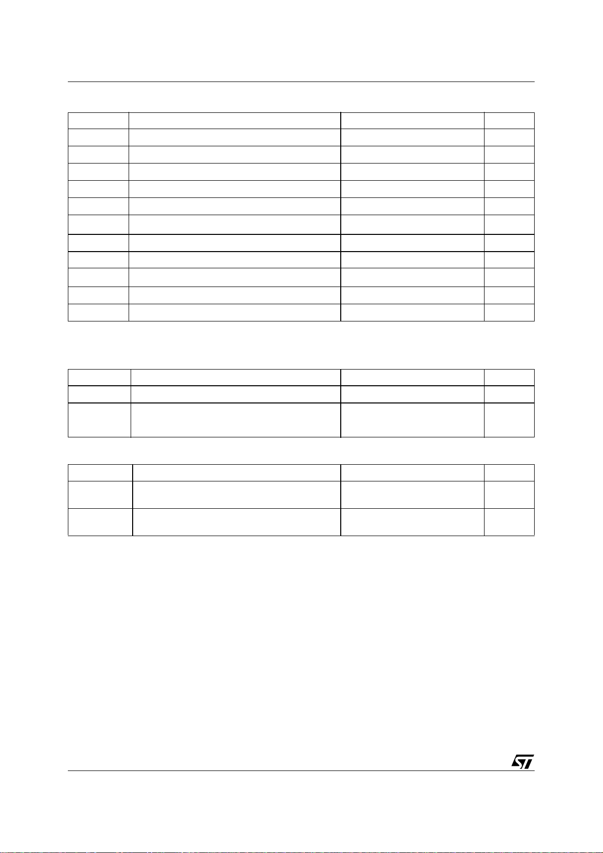
Figure 3. Absolute Maximum Ratings
Symbol Parameter Value Unit
Drain-source Voltage (VGS = 0) 500 V
V
DS
V
DGR
V
GS
I
D
I
D
I
DM
P
tot
dv/dt
T
stg
T
J
Note: 1. Pulse width limited by safe operating area
2. ISD ≤ 3A, di/dt ≤ 200 A/µs, VDD ≤ V(
Table 3. Thermal Data
Symbol Parameter Value Unit
R
thj-case
R
thj-amb
T
l
(1)
Drain- gate Voltage (RGS = 20 kΩ)500V
Gate-source Voltage ± 30 V
Drain Current (cont.) at TC = 25 °C 3 A
Drain Current (cont.) at TC = 100 °C 1.9 A
Drain Current (pulsed) 12 A
Total Dissipation at TC = 25 °C 50 W
Derating Factor 0.4 W°/C
(2)
Peak Diode Recovery voltage slope 4.5 V/ns
Storage Temperature -65 to 150 °C
Max. Operating Junction Temperature 150 °C
, Tj ≤ T
BR)DSS
JMAX
Thermal Resistance Junction-case Max 2.5 °C/W
Thermal Resistance Junction-ambient Max 100 °C/W
Maximum Lead Temperature For Soldering Purpose 275 °C
Table 4. Avalanche Characteristics
Symbol Parameter Max Value Unit
I
AR
E
AS
Avalanche Current, Repetitive or Not-Repetitive
(pulse width limited by T
max, δ < 1%)
j
Single Pulse Avalanche Energy
(starting T
= 25 °C; ID = IAR; VDD = 50 V)
j
3A
40 mJ
2/8
Page 3
Obsolete Product(s) - Obsolete Product(s)
STD3NB50/STD3NB50-1
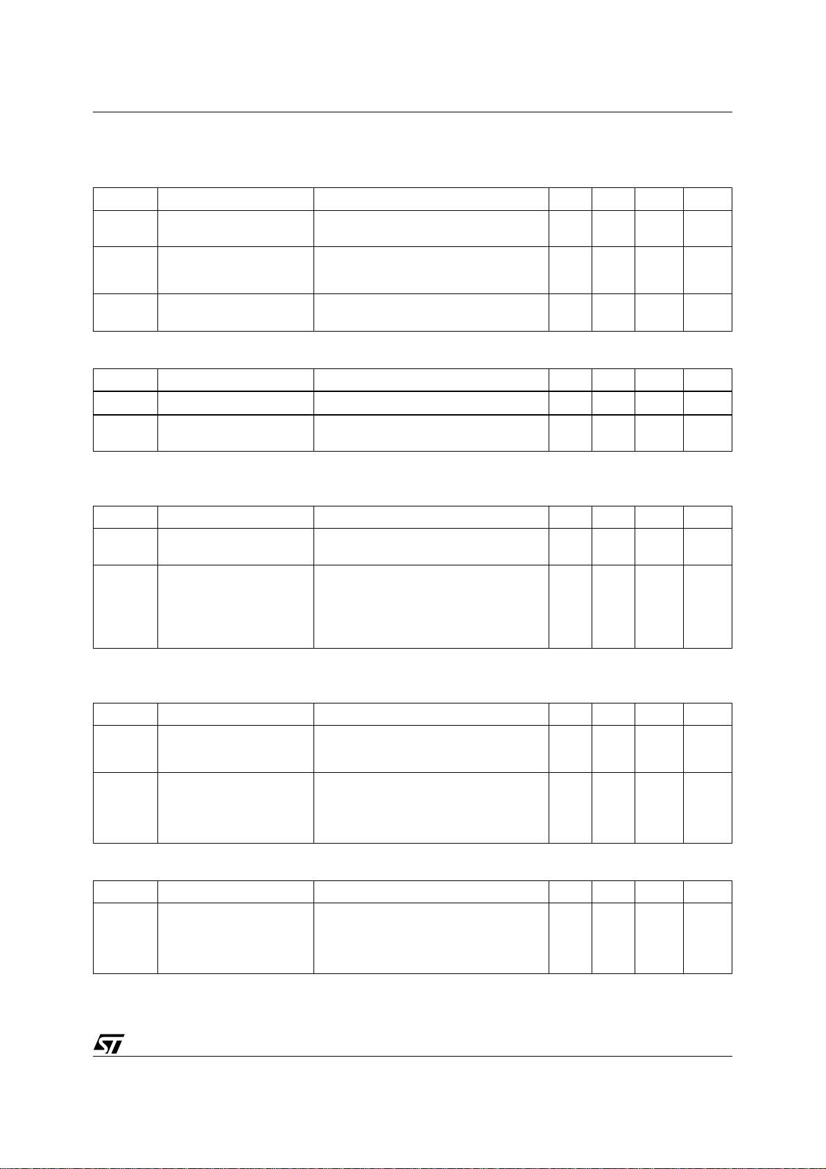
ELECTRICAL CHARACTERISTICS (T
= 25°C unless otherwise specified)
case
Table 5. Off
Symbol Parameter Test Conditions Min. Typ. Max. Unit
V
(BR)DSS
Drain-source
ID = 250 µA; VGS = 0 500 V
Breakdown Voltage
I
DSS
I
GSS
Table 6. On
Zero Gate Voltage VDS = Max Rating 1 µA
Drain Current (V
Gate-body Leakage
Current (V
(1)
DS
= 0) VDS = Max Rating; Tc = 125 °C 50 µA
GS
= ± 30 V ± 100 nA
V
GS
= 0)
Symbol Parameter Test Conditions Min. Typ. Max. Unit
V
GS(th)
R
DS(on)
Gate Threshold Voltage VDS = VGS; ID = 250 µA345V
Static Drain-source On
VGS = 10V; ID = 1.9 A 2.5 2.8 Ω
Resistance
Note: 1. Pulsed: Pulse duration = 300 µs, duty cycle 1.5 %
Table 7. Dynamic
Symbol Parameter Test Conditions Min. Typ. Max. Unit
(1)
g
fs
C
C
C
Forward
Transconductance
Input Capacitance VDS = 25 V; f = 1 MHz; VGS = 0 400 520 pF
iss
Output Capacitance 62 84 pF
oss
Reverse Transfer
rss
Capacitance
Note: 1. Pulsed: Pulse duration = 300 µs, duty cycle 1.5 %
VDS > I
D(on)
x R
DS(on)max
; ID = 1.9 A 2 2.3 S
7.5 10 pF
Table 8. Switching On
Symbol Parameter Test Conditions Min. Typ. Max. Unit
td(on) Turn-on Time V
tr Rise Time R
Q
Q
Q
Total Gate Charge VDD = 400 V; ID = 3.8 A; VGS = 10 V 15 21 nC
g
Gate-Source Charge 6.5 nC
gs
Gate-Drain Charge 5 nC
gd
= 250 V; ID = 1.9 A 11 17 ns
DD
= 4.7 Ω; VGS = 10 V 8 12 ns
G
Table 9. Switching Off
Symbol Parameter Test Conditions Min. Typ. Max. Unit
t
r(Voff)
Off-voltage Rise Time VDD = 400 V; ID = 3.8 A 8 12 ns
t
Fall Time RG = 4.7 Ω; VGS = 10 V 5 9 ns
f
t
Cross-over Time 14 20 ns
c
3/8
Page 4

Obsolete Product(s) - Obsolete Product(s)
STD3NB50/STD3NB50-1
Table 10. Source Drain Diode
Symbol Parameter Test Conditions Min. Typ. Max. Unit
I
SD
I
SDM
V
SD
t
rr
Q
I
RRAM
Note: 1. Pulse width limited by safe operating area
2. Pulsed: Pulse duration = 300 µs, duty cycle 1.5 %
Source-drain Current 3.8 A
(1)
Source-drain Current
(pulsed)
(2)
Forward On Voltage ISD = 3.8 A; VGS = 0 1.6 V
Reverse Recovery Time ISD = 3.8 A; di/dt = 100 A/µs
= 100 V; Tj = 150 °C
V
Reverse RecoveryCharge 980 µC
rr
Reverse RecoveryCharge 8 A
DD
245 ns
15.2 A
4/8
Page 5
Obsolete Product(s) - Obsolete Product(s)
STD3NB50/STD3NB50-1
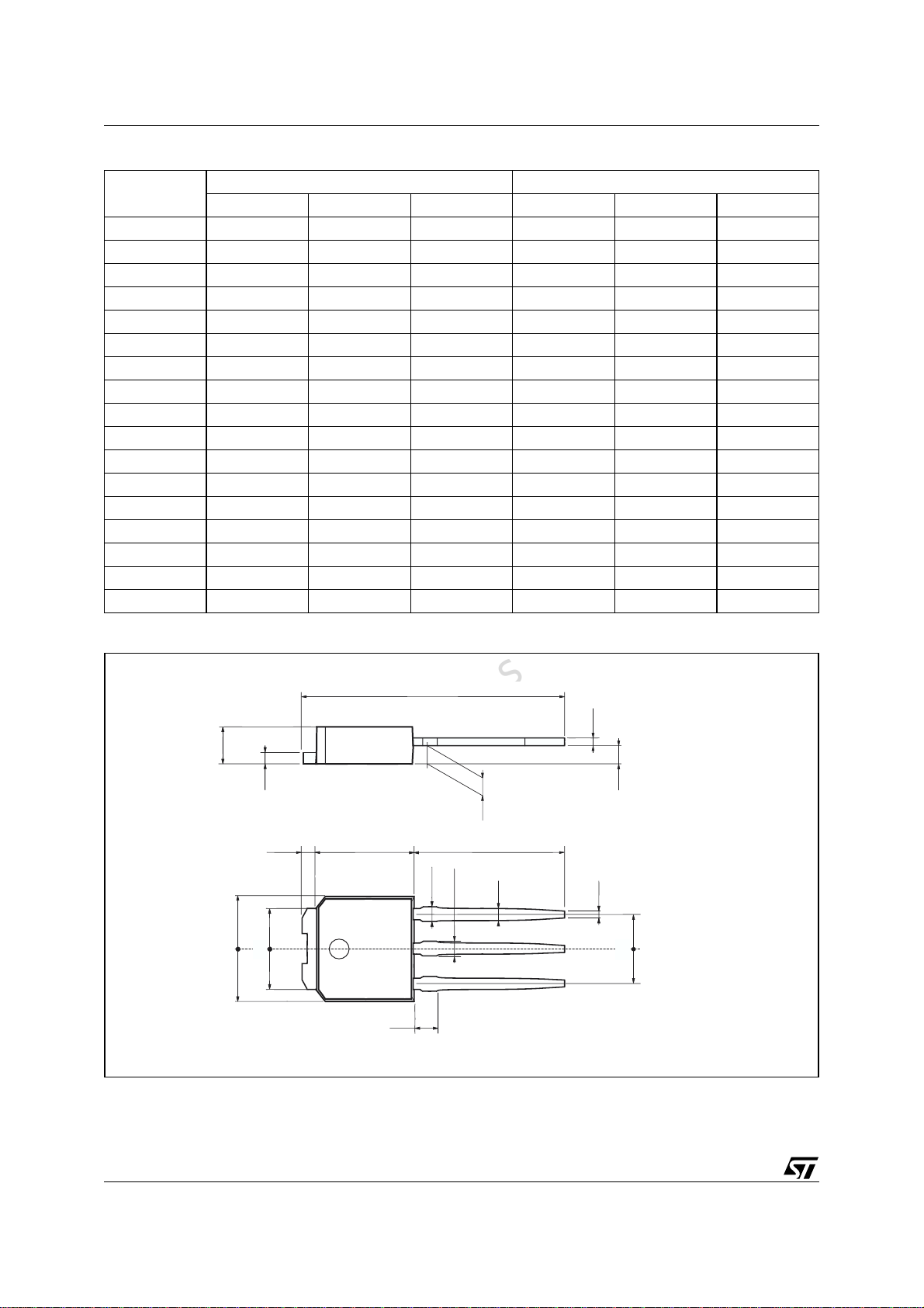
PACKAGE MECHANICAL
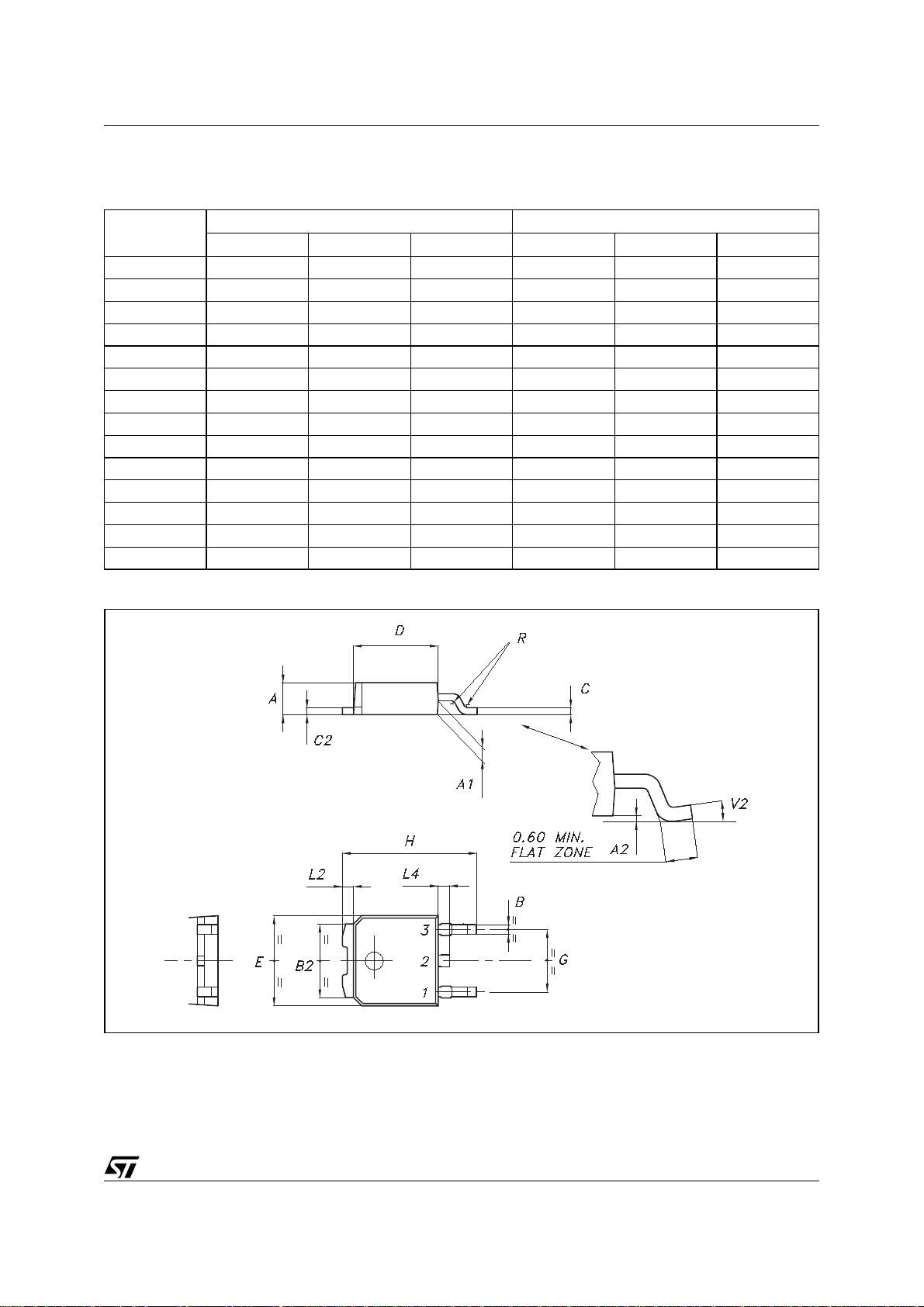
Table 11. DPAK Mechanical Data
Symbol
A 2.20 2.40 0.087 0.094
A1 0.90 1.10 0.035 0.043
A2 0.03 0.23 0.001 0.009
B 0.64 0.90 0.025 0.035
B2 5.20 5.40 0.204 0.213
C 0.45 0.60 0.018 0.024
C2 0.48 0.60 0.019 0.024
D 6.00 6.20 0.236 0.244
E 6.40 6.60 0.252 0.260
G 4.40 4.60 0.173 0.181
H 9.35 10.10 0.368 0.398
L2 0.8 0.031
L4 0.60 1.00 0.024 0.039
V2 0° 8° 0° 0°
Min Typ Max Min Typ Max
millimeters inches
Figure 4. DPAK Package Dimensions
P032P_B
Note: Drawing is not to scale.
5/8
Page 6
Obsolete Product(s) - Obsolete Product(s)
STD3NB50/STD3NB50-1
Table 12. IPAK Mechanical Data
Symbol
Typ Min Max Typ Min Max
A 2.2 2.4 0.086 0.094
A1 0.9 1.1 0.035 0.043
A3 0.7 1.3 0.027 0.051
B 0.64 0.9 0.025 0.031
B2 5.2 5.4 0.204 0.212
B3 0.85 0.033
B5 0.63 0.012
B6 0.95 0.037
C 0.45 0.6 0.017 0.023
C2 0.48 0.6 0.019 0.023
D 6 6.2 0.236 0.244
E 6.4 6.6 0.252 0.260
G 4.4 4.6 0.173 0.181
H 15.9 16.3 0.626 0.641
L 9 9.4 0.354 0.370
L1 0.8 1.2 0.031 0.047
L2 0.8 1 0.031 0.039
millimeters inches
Figure 5. IPAK Package Dimensions
H
C
A
A3
B5
G
E
= =
C2
L2
B2
= =
D
B3
2
1 3
L1
B6
A1
L
B
0068771-E
Note: Drawing is not to scale.
6/8
Page 7

Obsolete Product(s) - Obsolete Product(s)
REVISION HISTORY
Table 13. Revision History
Date Revision Description of Changes
May-1998 1 First Issue
14-Apr-2004 2 Stylesheet update. No content change.
STD3NB50/STD3NB50-1
7/8
Page 8

Obsolete Product(s) - Obsolete Product(s)
STD3NB50/STD3NB50-1
Information furnished is believed to be accurate and reliable. However, STMicroelectronics assumes no responsibility for the consequences
of use of such information nor for any infringement of patents or other rights of third parties which may result from its use. No license is granted
by implication or otherwise under any patent or patent rights of STMicroelectronics. Specifications mentioned in this publication are subject
to change without notice. This publication supersedes and replaces all information previously supplied. STMicroelectronics products are not
authorized for use as critical components in life support devices or systems without express written approval of STMicroelectronics.
The ST logo is a registered trademark of STMicroelectronics.
All other names are the property of their respective owners
© 2004 STMicroelectronics - All rights reserved
STMicroelectronics GROUP OF COMPANIES
Australia - Belgium - Brazil - Canada - China - Czech Republic - Finland - France - Germany - Hong Kong - India - Israel - Italy - Japan -
8/8
Malaysia - Malta - Morocco - Singapore - Spain - Sweden - Switzerland - United Kingdom - United States
www.st.com
 Loading...