

Page 1
N - CHANNEL 30V - 0.013 Ω - 38A TO-252
TYPE V
DSS
ST D38N F 03L 30 V < 0.019 Ω 38 A
■ TYPICALR
■ OPTIMIZEDFORHIGH SWTICHING
DS(on)
= 0.013 Ω
OPERATIONS
■ LOW THRESHOLDDRIVE
■ ADDSUFFIX ”T4” FORORDERING INTAPE
& REEL
R
DS(o n)
I
D
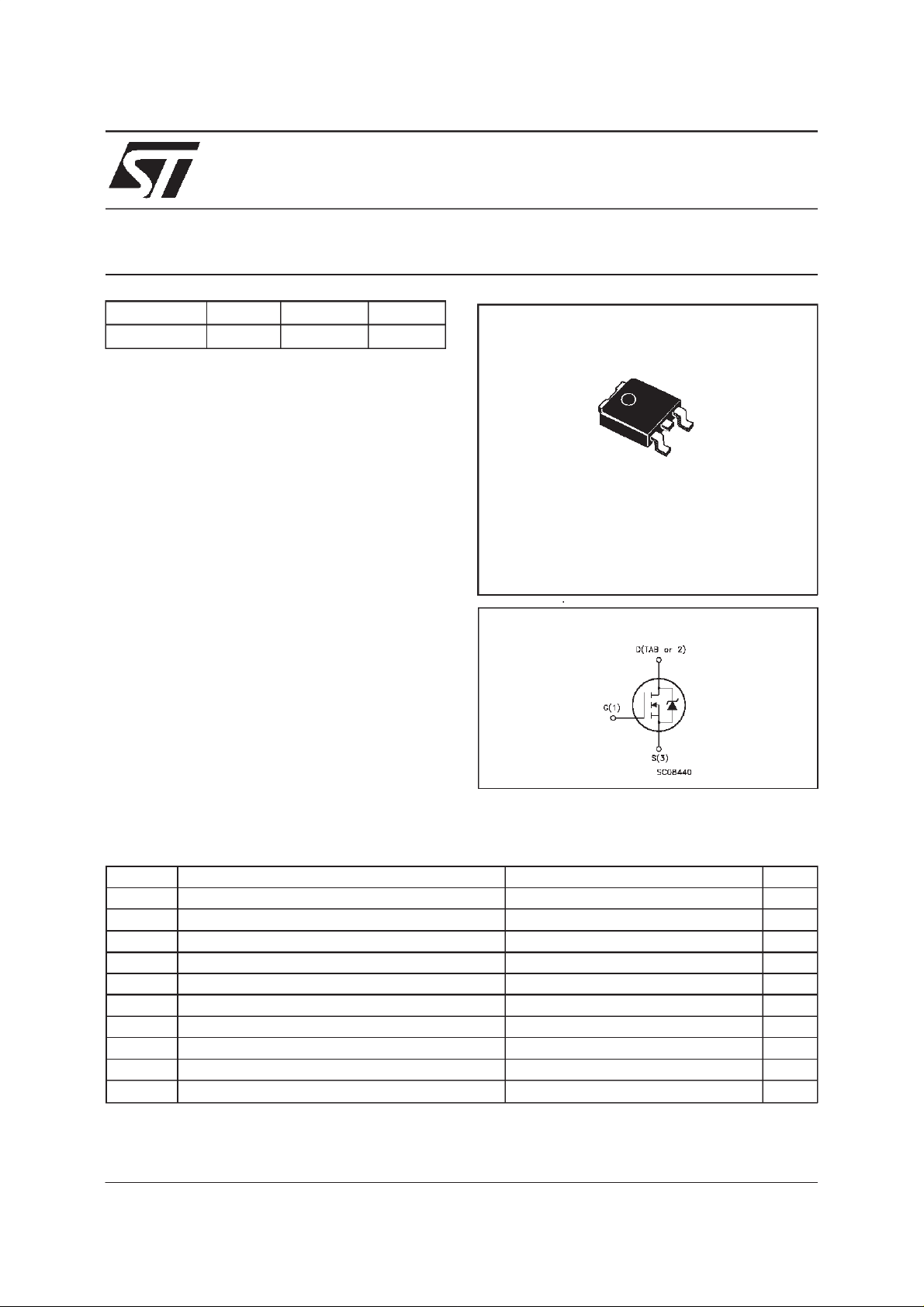
STD38NF03L
STripFET POWER MOSFET
PRELIMINARY DATA
3
1
DESCRIPTION
This Power MOSFET is the latest developmentof
STMicroelectronics unique ”Single Feature
Size” strip-based process. The resulting transi-
DPAK
TO-252
(Suffix ”T4”)
stor shows extremelyhigh packing density forlow
on-resistance, rugged avalanche characteristics
and less critical alignment steps therefore a remarkablemanufacturingreproducibility.
INTERNAL SCHEMATIC DIAGRAM
APPLICATIONS
■ HIGHCURRENT, HIGH SPEEDSWITCHING
■ MOTORCONTROL, AUDIOAMPLIFIERS
■ DC-DC& DC-AC CONVERTERS
ABSOLUTE MAXIMUM RATINGS
Symbol Parameter Value Uni t
V
V
V
I
D
I
DM
P
T
(•) Pulse width limitedby safe operating area (*)Value limitedby the package
Dra in- sour c e Volta ge (VGS=0) 30 V
DS
Drain- gate Voltage (RGS=20kΩ)30V
DGR
Gate-s ource Voltage ± 20 V
GS
(*) Dra in Cu rr ent (conti nuous) at Tc=25oC38A
Dra in Cu rr ent (conti nuous) at Tc= 100oC27A
I
D
(•) D ra in Cu rr ent (pulse d) 152 A
Tot al Dissipatio n at Tc=25oC45W
tot
Der ati ng Fa c t or 0.3 W/
St orage Tempe rat ure -65 to 175
stg
Max. Operating Jun ct ion Temperatur e 175
T
j
o
C
o
C
o
C
March 2000
1/6
Page 2
STD38NF03L
THERMAL DATA
R
thj-pcb
R
thj-amb
R
thj-sink
T
Ther mal Resistanc e Junct ion-PC Board Max
Ther mal Resistanc e Junct ion-ambie nt Max
Ther mal Resistanc e Case-sink Ty p
Maximum Lead Temper a tu r e For Soldering Purpose
l
3.33
62.5
1.5
300
o
C/W
o
C/W
o
C/W
o
C
ELECTRICAL CHARACTERISTICS
=25oC unless otherwisespecified)
(T
case
OFF
Symbol Parameter Test Conditions Min. Typ. Max. U nit
V
(BR)DSS
Drain-source
ID=250µAVGS=0 30 V
Break dow n Vo lt age
I
DSS
I
GSS
Zero Gate Volta ge
Drain Curre nt (V
GS
Gat e- bod y Leakag e
Current (V
DS
=0)
=0)
V
=MaxRating
DS
=MaxRating Tc= 125oC
V
DS
V
= ± 20 V ± 100 nA
GS
1
10
ON(∗)
Symbol Parameter Test Conditions Min. Typ. Max. U nit
V
GS(th)
R
DS(on)
I
D(on)
Gate Threshold Voltage VDS=VGSID= 250 µA11.72.5V
Sta t ic Drain-s our c e On
Resistance
VGS=10V ID=19A
=4.5V ID=19A
V
GS
On State Drain Current VDS>I
D(on)xRDS(on)max
0.013
0.016
38 A
0.019
0.023ΩΩ
VGS=10V
DYNAMIC
Symbol Parameter Test Conditions Min. Typ. Max. U nit
g
(∗)Forward
fs
Tr ansc on duc tance
C
C
C
Input Capaci t ance
iss
Out put Capac itance
oss
Reverse Transfer
rss
Capacit a nc e
VDS>I
D(on)xRDS(on)maxID
=19A 28 S
VDS=20V f=1MHz VGS= 0 V 1450
390
155
µ
µA
pF
pF
pF
A
2/6
Page 3

STD38NF03L
ELECTRICAL CHARACTERISTICS
(continued)
SWITCHING ON
Symbol Parameter Test Conditions Min. Typ. Max. U nit
t
d(on)
Tur n-on Delay T ime
Rise Time
t
r
VDD=15V ID= 27.5 A
R
=4.7
G
Ω
VGS=4.5V
25
280
(Resis t iv e Load, see fig. 3)
Q
Q
Q
Tot al Gate Charge
g
Gat e- Source Charge
gs
Gate-Drain Charge
gd
VDD=24V ID=55A VGS=4.5V 27
11
12
36 nC
SWITCHING OFF
Symbol Parameter Test Conditions Min. Typ. Max. U nit
t
d(off)
Tur n-of f Dela y Tim e
t
Fall T ime
f
VDD=15V ID= 27.5 A
=4.7 Ω VGS=4.5V
R
G
60
240
(Resis t iv e Load, see fig. 3)
t
r(Voff)
t
t
Off-voltage Rise Time
Fall T ime
f
Cross-over Time
c
V
R
=24V ID=55A
CLAM P
=4.7 Ω VGS=4.5V
G
(Indu ct iv e Load, see fig. 5)
140
200
350
SOURCEDRAINDIODE
Symbol Parameter Test Conditions Min. Typ. Max. U nit
I
V
I
SDM
SD
Q
I
RRM
SD
t
Source-drain Current
(•)
Source-drain Current
38
152
(pulsed)
(∗)ForwardOnVoltage ISD=38A VGS=0 1.5 V
Reverse Recovery
rr
Time
Reverse Recovery
rr
ISD= 55 A di / dt = 100 A/µs
=15V Tj=150oC
V
DD
(see test circuit, fig. 5)
45
52
Charge
Reverse Recovery
2.3
Current
ns
ns
nC
nC
ns
ns
ns
ns
ns
A
A
ns
nC
A
(∗) Pulsed: Pulse duration = 300 µs, duty cycle 1.5%
(•) Pulse width limited by safe operatingarea
3/6
Page 4

STD38NF03L
Fig. 1:
UnclampedInductiveLoad Test Circuit
Fig. 3: SwitchingTimes Test Circuits For
ResistiveLoad
Fig. 2:
UnclampedInductive Waveform
Fig. 4: Gate Chargetest Circuit
Fig. 5:
Test CircuitFor InductiveLoad Switching
And Diode Recovery Times
4/6
Page 5

TO-252 (DPAK) MECHANICAL DATA
STD38NF03L
DIM.
mm inch
MIN. TYP. MAX. MIN. TYP. MAX.
A 2.2 2.4 0.086 0.094
A1 0.9 1.1 0.035 0.043
A2 0.03 0.23 0.001 0.009
B 0.64 0.9 0.025 0.035
B2 5.2 5.4 0.204 0.212
C 0.45 0.6 0.017 0.023
C2 0.48 0.6 0.019 0.023
D 6 6.2 0.236 0.244
E 6.4 6.6 0.252 0.260
G 4.4 4.6 0.173 0.181
H 9.35 10.1 0.368 0.397
L2 0.8 0.031
L4 0.6 1 0.023 0.039
H
A
E
C2
L2
B2
==
==
DETAIL”A”
D
2
13
L4
A1
C
A2
DETAIL”A”
B
G
==
0068772-B
5/6
Page 6

STD38NF03L
Information furnishedis believed tobeaccurateand reliable.However, STMicroelectronics assumes no responsibilityforthe consequences
of use of such information nor for any infringement of patents or other rights of third parties which may result from its use. No license is
granted by implication or otherwise under any patent or patent rights of STMicroelectronics. Specificationmentioned in this publicationare
subjecttochange without notice. This publication supersedes and replaces all information previouslysupplied. STMicroelectronics products
are not authorized for use as critical components in lifesupport devicesor systemswithout express written approval of STMicroelectronics.
The STlogo is a trademark of STMicroelectronics
1999 STMicroelectronics – Printed in Italy – All Rights Reserved
STMicroelectronics GROUP OF COMPANIES
Australia - Brazil - China - Finland - France - Germany - Hong Kong - India - Italy - Japan - Malaysia - Malta - Morocco -
6/6
Singapore - Spain - Sweden - Switzerland - United Kingdom - U.S.A.
http://www.st.com
.
 Loading...