

Page 1
STD30PF03L
STD30PF03L-1
P-CHANNEL 30V - 0.025Ω - 24A DPAK/IPAK
STripFET™ II POWER MOSFET
PRELIMINARY DATA
TYPE V
STD30PF03 L
STD30PF03 L-1
■ TYPICAL R
■ STANDARD OUTLI N E FOR EAS Y
DS(on)
DSS
30 V
30 V
= 0.025Ω
R
DS(on)
< 0.028Ω
< 0.028Ω
I
D
24 A
24 A
AUTOMATED SURFACE MOUNT ASSEMBLY
■ LOW THRESHOLD DRIVE
■ LOW GATE CHARGE
■ EXTREMELY LOW FIGURE OF MERIT
(R
DS(on) * Qg
)
DESCRIPTION
This Power MOSFET is the latest dev elo pment of
STMicroelectronics unique “Single Feature
Size™” strip-based process. The resulting transistor shows extremely high packing density for low
on-resistance and low gate charge.
APPLICATIONS
■ DC-DC CONVERTERS
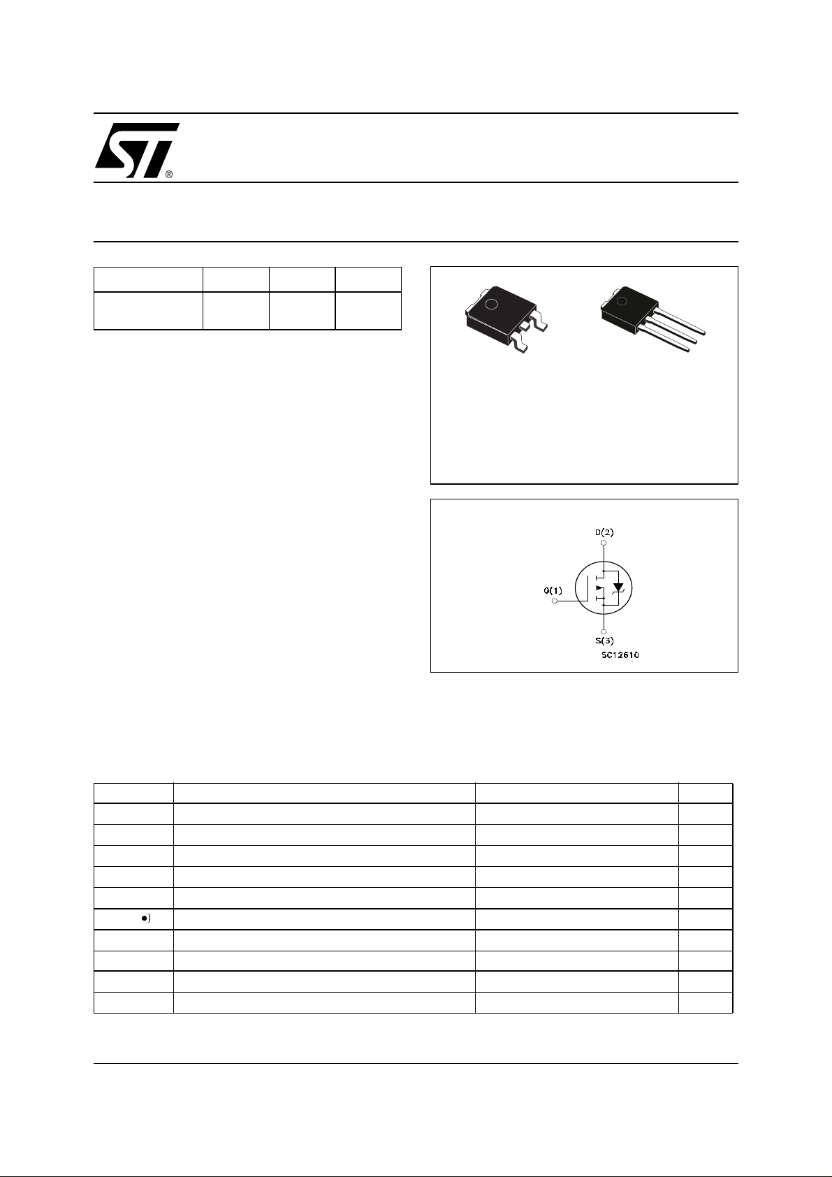
3
DPAK
1
IPAK
1
INTERNAL SCHEMATIC DIAGRAM
3
2
ABSOLUTE MAXIMUM RATINGS
Symbol Parameter Value Unit
V
DS
V
DGR
V
GS
I
(#) Drain Current (continuous) at TC = 25°C
D
ID (#) Drain Current (continuous) at TC = 100°C
I
DM
P
TOT
T
stg
T
j
(●) Pulse width limited by safe operating area
(#) Curre nt lim i ted by wire bonding
May 2002
Drain-source Voltage (VGS = 0)
Drain-gate Voltage (RGS = 20 kΩ)
Gate- source Voltage ± 16 V
(l)
Drain Current (pulsed) 96 A
Total Dissipation at TC = 25°C
Derating Factor 0.47 W/°C
Storage Temperature – 55 to 175 °C
Max. Operating Junction Temperature 175 °C
Note:For the P-CHANNEL MOSFET actual polarity of voltages and
30 V
30 V
24 A
24 A
70 W
current has to be reve rsed
1/8
Page 2
STD30PF03L - STD30PF03L-1
THERMA L D ATA
Rthj-case Thermal Resistance Junction-case Max 2.14 °C/W
Rthj-amb Thermal Resistance Junction-ambient Max 100 °C/W
T
j
AVALANCHE CHARACTERISTICS
Symbol Parameter Max Value Unit
I
AR
E
AS
ELECTRICAL CHARACTERISTICS (TCASE = 25 °C UNLESS OTHERWISE SPECIFIED)
OFF
Symbol Parameter Test Conditions Min. Typ. Max. Unit
V
(BR)DSS
I
DSS
I
GSS
Maximum Operating Junction Temperature 275 °C
Avalanche Current, Repetitive or Not-Repetitive
(pulse width limited by T
max)
j
Single Pulse Avalanche Energy
(starting T
Drain-source
= 25 °C, ID = IAR, VDD = 25 V)
j
ID = 250 µA, VGS = 0 30 V
24 A
350 mJ
Breakdown Voltage
Zero Gate Voltage
Drain Current (V
GS
Gate-body Leakage
Current (V
DS
= 0)
= 0)
V
= Max Rating
DS
V
= Max Rating, TC = 125 °C
DS
V
= ± 16 V ±100 nA
GS
1µA
10 µA
ON
(1)
Symbol Parameter Test Conditions Min. Typ. Max. Unit
V
GS(th)
R
DS(on)
Gate Threshold Voltage
Static Drain-source On
Resistance
V
= VGS, ID = 250µA
DS
VGS = 10 V, ID = 12 A
VGS = 5 V, ID = 12 A
1V
0025 0.028 Ω
0.032 0.040 Ω
DYNAMIC
Symbol Parameter Test Conditions Min. Typ. Max. Unit
(1) Forward Transconductance VDS = 15 V, ID= 12 A 23 S
g
fs
C
iss
C
oss
C
rss
Input Capacitance
Output Capacitance 345 pF
Reverse Transfer
Capacitance
V
= 25V, f = 1 MHz, VGS = 0
DS
1670 pF
120 pF
2/8
Page 3
STD30PF03L - STD30PF03L-1
ELECTRICAL CHARACTERISTICS (CONTINUED)
SWITCHING ON
Symbol Parameter Test Conditions Min. Typ. Max. Unit
V
t
d(on)
Q
Q
Q
t
r
g
gs
gd
Turn-on Delay Time
Rise Time 122 ns
Total Gate Charge
Gate-Source Charge
Gate-Drain Charge
SWITCHING OFF
Symbol Parameter Test Conditions Min. Typ. Max. Unit
t
d(off)
t
f
Turn-off-Delay Time
Fall Time
SOURCE DRAIN DIODE
Symbol Parameter Test Conditions Min. Typ. Max. Unit
I
SD
I
SDM
VSD (1)
t
rr
Q
rr
I
RRM
Note: 1. Pulsed: Pu l se duration = 300 µs, duty c yc l e 1.5 %.
2. Pulse width li mited by safe operating area.
Source-drain Current 24 A
(2)
Source-drain Current (pulsed) 96 A
Forward On Voltage
Reverse Recovery Time
Reverse Recovery Charge
Reverse Recovery Current
= 24 V, ID = 24 A
DD
R
= 4.7Ω VGS = 4.5V
G
(see test circuit, Figure 3)
VDD = 15 V, ID = 24 A,
VGS = 5 V
VDD = 24 V, ID = 24 A,
RG=4.7Ω, V
GS
= 4.5V
(see test circuit, Figure 3)
ISD = 24 A, VGS = 0
= 24 A, di/dt = 100 A/µs,
I
SD
VDD = 24 V, Tj = 150 °C
(see test circuit, Figure 5)
64 ns
18.5
25 nC
5.5
11
36
26
2.3 V
40
52
2.6
nC
nC
ns
ns
ns
µC
A
3/8
Page 4

STD30PF03L - STD30PF03L-1
Fig. 2: Unclamped Inductive WaveformFig. 1: Unclamped Inductive Load Test Circuit
Fig. 3: Switching Times Test Circuit For
Resistive Load
Fig. 5: Test Circuit For Inductive Load Switching
And Diode Recovery Times
Fig. 4: Gate Charge test Circuit
4/8
Page 5

STD30PF03L - STD30PF03L-1
TO-252 (DPAK) MECHANICAL DATA
DIM.
A 2.20 2.40 0.087 0.094
A1 0.90 1.10 0.035 0.043
A2 0.03 0.23 0.001 0.009
B 0.64 0.90 0.025 0.035
B2 5.20 5.40 0.204 0.213
C 0.45 0.60 0.018 0.024
C2 0.48 0.60 0.019 0.024
D 6.00 6.20 0.236 0.244
E 6.40 6.60 0.252 0.260
G 4.40 4.60 0.173 0.181
H 9.35 10.10 0.368 0.398
L2 0.8 0.031
L4 0.60 1.00 0.024 0.039
V2 0
MIN. TYP. MAX. MIN. TYP. MAX.
o
mm inch
o
8
o
0
o
0
P032P_B
5/8
Page 6

STD30PF03L - STD30PF03L-1
TO-251 (IPAK) MECHANICAL DAT A
DIM.
MIN. TYP. MAX. MIN. TYP. MAX.
mm inch
A 2.2 2.4 0.086 0.094
A1 0.9 1.1 0.035 0.043
A3 0.7 1.3 0.027 0.051
B 0.64 0.9 0.025 0.031
B2 5.2 5.4 0.204 0.212
B3 0.85 0.033
B5 0.3 0.012
B6 0.95 0.037
C 0.45 0.6 0.017 0.023
C2 0.48 0.6 0.019 0.023
D 6 6.2 0.236 0.244
E 6.4 6.6 0.252 0.260
G 4.4 4.6 0.173 0.181
H 15.9 16.3 0.626 0.641
L 9 9.4 0.354 0.370
L1 0.8 1.2 0.031 0.047
L2 0.8 1 0.031 0.039
H
C
A
6/8
C2
E
= =
L2
B2
= =
D
B3
2
1 3
L1
A1
L
B6
A3
B
B5
G
= =
0068771-E
Page 7

STD30PF03L - STD30PF03L-1
DPAK FOOTPRINT
All dimensions are in millimeters
TAPE AND REEL SHIPMENT (suffix ”T4”)*
TUBE SHIPMENT (no suffix)*
All dimensions
are in millimeters
REEL MECHANICAL DATA
DIM.
A 330 12.992
B 1.5 0.059
C 12.8 13.2 0.504 0.520
D 20.2 0.795
G 16.4 18.4 0.645 0.724
N 50 1.968
T 22.4 0.881
mm inch
MIN. MAX. MIN. MAX.
TAPE MECHANICAL DATA
DIM.
A0 6.8 7 0.267 0.275
B0 10.4 10.6 0.409 0.417
B1 12.1 0.476
D 1.5 1.6 0.059 0.063
D1 1.5 0.059
E 1.65 1.85 0.065 0.073
F 7.4 7.6 0.291 0.299
K0 2.55 2.75 0.100 0.108
P0 3.9 4.1 0.153 0.161
P1 7.9 8.1 0.311 0.319
P2 1.9 2.1 0.075 0.082
R 40 1.574
W 15.7 16.3 0.618 0.641
* on sales type
mm inch
MIN. MAX. MIN. MAX.
BASE QTY BULK QTY
2500 2500
7/8
Page 8

STD30PF03L - STD30PF03L-1
8/8
Information furnished is believed to be accurate and reliable. However, STMicroelectronics assumes no responsibility for the
consequences of use of su ch in formation nor for any in fringement of patents or other rights of third parties w hich may result from
its use. No license is granted by implication or otherwise under any patent or patent rights of STMicroelectronics. Specifications
mentioned in this publication are subject to change without notice. This publication supersedes and replaces all information
previously suppli ed. STMi croelect ronics pr oducts are not author ized for use as cr itical component s in li fe suppo rt devi ces or
systems without express written approval of STMicroelectronics.
Australia - Brazil - Canada - China - Finland - France - Germany - Hong Kong - India - Israel - Italy - Japan - Malaysia - Malta - Morocco
© The ST logo is a registered trademark of STMicroelectronics
© 2002 STMicroelectronics - Printed in Italy - All Rights Reserved
Singapore - Spain - Sweden - Switzerland - United Kingdom - United States.
STMicroelectronics GROUP OF COMPANIES
© http://www.st.com
 Loading...