

Page 1
1/10July 2002
STD30NF06L
N-CHANNEL 60V - 0.022Ω - 35A DPAK/IPAK
STripFET™ POWER MOSFET
(1) ISD ≤38A, di/dt ≤400A/µs, VDD ≤ V
(BR)DSS
, Tj ≤ T
JMAX.
■ TYPICAL R
DS
(on) = 0.022Ω
■ EXCEPTIONAL dv/dt CAPABILI TY
■ LOGIC LEVEL GATE D R IVE
■ ADD SUFFIX “T4” FOR ORDERING IN TAPE &
REEL
■ ADD SUFFIX “-1” FOR ORDERING IN IPAK
■ CHARACTERIZATION ORIENTED FOR
AUTOMOTIVE APPLICATIONS
DESCRIPTION
This Power Mosfet is the latest development of
STMicroelectronics unique “Single Feature
Size
™” strip-based process. The re sulting tran-
sistor shows extremely high packing density for
low on-resistance, rugged avalance characteristics and less critical alignment steps therefore a remarkable manufacturing reproducibility.
APPLICATIONS
■ HIGH-EFFICIENCY DC-DC CONVERTERS
■ MOTOR CONTROL, AUDIO AMPLIFIERS
■ DC-DC & DC-AC CONVERTERS
■ AUTOMOTIVE
ABSOLUTE MAXIMUM RATINGS
(●) Pulse width limited by safe operating area
TYPE V
DSS
R
DS(on)
I
D
STD30NF06L 60 V <0.028Ω 35 A
Symbol Parameter Value Unit
V
DS
Drain-source Voltage (VGS = 0)
60 V
V
DGR
Drain-gate Voltage (RGS = 20 kΩ)
60 V
V
GS
Gate- source Voltage ± 20 V
I
D
Drain Current (continuous) at TC = 25°C
35 A
I
D
Drain Current (continuous) at TC = 100°C
25 A
I
DM
(l)
Drain Current (pulsed) 140 A
P
TOT
Total Dissipation at TC = 25°C
70 W
Derating Factor 0.46 W/°C
dv/dt (1) Peak Diode Recovery voltage slope 25 V/ns
T
stg
Storage Temperature
– 55 to 175 °C
T
j
Operating Junction Temperature
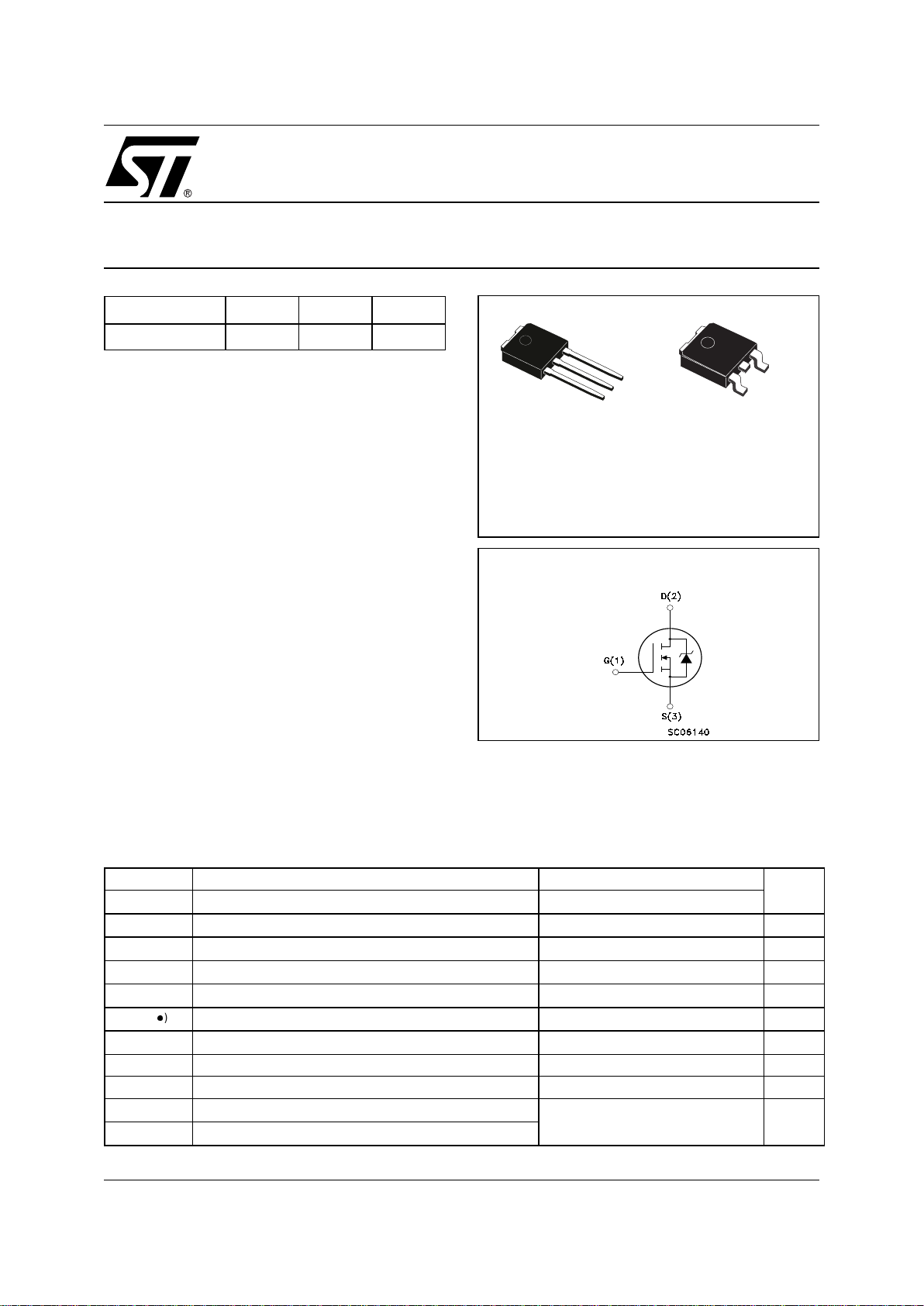
DPAK
3
2
1
1
3
IPAK
INTERNAL SCHEMATIC DIAGRAM
Page 2
STD30NF06L
2/10
THERMA L D ATA
AVALANCHE CHARACTERISTICS
ELECTRICAL CHARACTERISTICS (TCASE = 25 °C UNLESS OTHERWISE SPECIFIED)
OFF
ON
(1)
DYNAMIC
Rthj-case Thermal Resistance Junction-case Max 2.14 °C/W
Rthj-amb Thermal Resistance Junction-ambient Max 100 °C/W
T
l
Maximum Lead Temperature For Soldering Purpose 275 °C
Symbol Parameter Max Value Unit
I
AR
Avalanche Current, Repetitive or Not-Repetitive
(pulse width limited by T
j
max)
35 A
E
AS
Single Pulse Avalanche Energy
(starting T
j
= 25 °C, ID = IAR, VDD = 50 V)
150 mJ
Symbol Parameter Test Conditions Min. Typ. Max. Unit
V
(BR)DSS
Drain-source
Breakdown Voltage
ID = 250 µA, VGS = 0 60 V
I
DSS
Zero Gate Voltage
Drain Current (V
GS
= 0)
V
DS
= Max Rating
1µA
V
DS
= Max Rating, TC = 125 °C
10 µA
I
GSS
Gate-body Leakage
Current (V
DS
= 0)
V
GS
= ± 20 V ±100 nA
Symbol Parameter Test Conditions Min. Typ. Max. Unit
V
GS(th)
Gate Threshold Voltage
V
DS
= VGS, ID = 250 µA
1 1.7 2.5 V
R
DS(on)
Static Drain-source On
Resistance
VGS = 5 V, ID = 18 A
0.025 0.03 Ω
VGS = 10 V, ID = 18 A
0.022 0.028 Ω
Symbol Parameter Test Conditions Min. Typ. Max. Unit
g
fs
(1) Forward Transconductance VDS > =15 V , ID=15 A 25 S
C
iss
Input Capacitance
V
DS
= 25 V, f = 1 MHz, VGS = 0
1600 pF
C
oss
Output Capacitance 215 pF
C
rss
Reverse Transfer
Capacitance
60 pF
Page 3

3/10
STD30NF06L
ELECTRICAL CHARACTERISTICS (CONTINUED)
SWITCHING ON
SWITCHING OFF
SOURCE DRAIN DIODE
Note: 1. Pulsed: Pu l se duration = 300 µs, duty cycle 1.5 %.
2. Pulse width li mited by safe operating ar ea.
Symbol Parameter Test Conditions Min. Typ. Max. Unit
t
d(on)
Turn-on Delay Time
V
DD
= 30 V, ID = 18 A
R
G
= 4.7Ω VGS = 4.5 V
(see test circuit, Figure 3)
30 ns
t
r
Rise Time 105 ns
Q
g
Q
gs
Q
gd
Total Gate Charge
Gate-Source Charge
Gate-Drain Charge
VDD = 48 V, ID = 38 A,
VGS = 5 V
23
7
10
31 nC
nC
nC
Symbol Parameter Test Conditions Min. Typ. Max. Unit
t
d(off)
t
f
Turn-off-Delay Time
Fall Time
VDD = 30 V, ID = 18 A,
RG=4.7Ω, V
GS
= 4.5 V
(see test circuit, Figure 3)
65
25
ns
ns
Symbol Parameter Test Conditions Min. Typ. Max. Unit
I
SD
Source-drain Current 35 A
I
SDM
(2)
Source-drain Current (pulsed) 140 A
VSD (1)
Forward On Voltage
ISD = 35 A, VGS = 0
1.5 V
t
rr
Q
rr
I
RRM
Reverse Recovery Time
Reverse Recovery Charge
Reverse Recovery Current
I
SD
= 38 A, di/dt = 100 A/µs,
V
DD
= 15 V, Tj = 150°C
(see test circuit, Figure 5)
70
140
4
ns
nC
A
Normalized Thermal ImpedenceSafe Operating Area
Page 4

STD30NF06L
4/10
Output Characteristics
Gate Charge vs Gate-source Voltage
Transconductance Static Drain-source On Resistance
Transfer Characteristics
Capacitance Variations
Page 5

5/10
STD30NF06L
Normalized Gate Threshold Volta ge vs
Temperature
Normalized Drain-Source Break down vs
Temperature
Source-drain Diode Forward Characteristics
Normalized On Resistance vs Temperature
Page 6

STD30NF06L
6/10
Fig. 5: Test Circuit For Inductive Load Switching
And Diode Recovery Times
Fig. 4: Gate Charge test Circuit
Fig. 2: Unclamped Inductive WaveformFig. 1: Unclamped Inductive Load Test Circuit
Fig. 3: Switching Times Test Circuit For
Resistive Load
Page 7
7/10
STD30NF06L
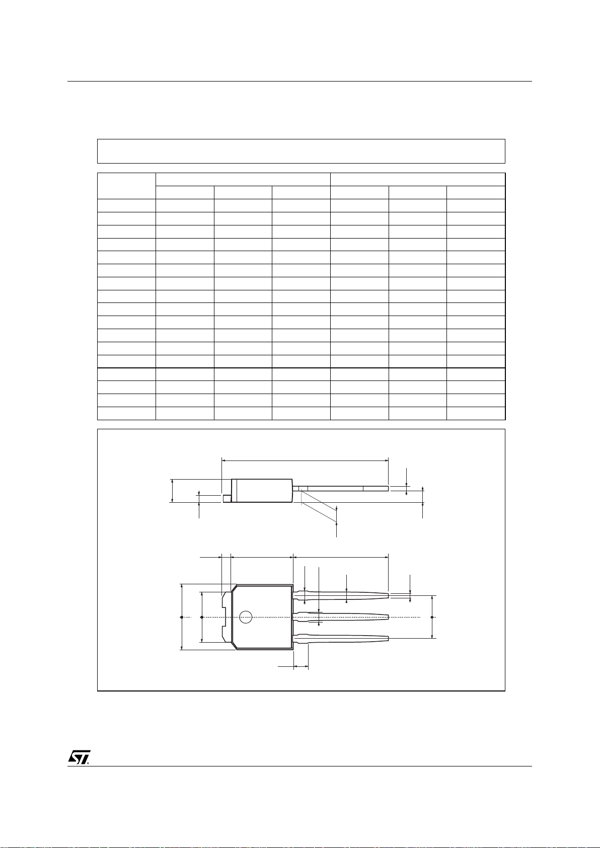
DIM.
mm inch
MIN. TYP. MAX. MIN. TYP. MAX.
A 2.2 2.4 0.086 0.094
A1 0.9 1.1 0.035 0.043
A3 0.7 1.3 0.027 0.051
B 0.64 0.9 0.025 0.031
B2 5.2 5.4 0.204 0.212
B3 0.85 0.033
B5 0.3 0.012
B6 0.95 0.037
C 0.45 0.6 0.017 0.023
C2 0.48 0.6 0.019 0.023
D 6 6.2 0.236 0.244
E 6.4 6.6 0.252 0.260
G 4.4 4.6 0.173 0.181
H 15.9 16.3 0.626 0.641
L 9 9.4 0.354 0.370
L1 0.8 1.2 0.031 0.047
L2 0.8 1 0.031 0.039
A
C2
C
A3
H
A1
D
L
L2
L1
1 3
= =
B3
B
B6
B2
E
G
= =
= =
B5
2
TO-251 (IPAK) MECHANICAL DAT A
0068771-E
Page 8

STD30NF06L
8/10
DIM.
mm inch
MIN. TYP. MAX. MIN. TYP. MAX.
A 2.20 2.40 0.087 0.094
A1 0.90 1.10 0.035 0.043
A2 0.03 0.23 0.001 0.009
B 0.64 0.90 0.025 0.035
B2 5.20 5.40 0.204 0.213
C 0.45 0.60 0.018 0.024
C2 0.48 0.60 0.019 0.024
D 6.00 6.20 0.236 0.244
E 6.40 6.60 0.252 0.260
G 4.40 4.60 0.173 0.181
H 9.35 10.10 0.368 0.398
L2 0.8 0.031
L4 0.60 1.00 0.024 0.039
V2 0
o
8
o
0
o
0
o
P032P_B
TO-252 (DPAK) MECHANICAL DATA
Page 9

STD30NF06L
9/10
TAPE AND REEL SHIPMENT (suffix ”T4”)*
TUBE SHIPMENT (no suffix)*
DPAK FOOTPRINT
DIM.
mm inch
MIN. MAX. MIN. MAX.
A 330 12.992
B 1.5 0.059
C 12.8 13.2 0.504 0.520
D 20.2 0.795
G 16.4 18.4 0. 645 0.724
N 50 1.968
T 22.4 0.881
BASE QTY BULK QTY
2500 2500
REEL MECHANICAL DATA
DIM.
mm inch
MIN. MAX. MIN. MAX.
A0 6.8 7 0.267 0.275
B0 10.4 10.6 0.409 0.417
B1 12.1 0.476
D 1.5 1.6 0.059 0.063
D1 1.5 0.059
E 1.65 1.85 0.065 0.073
F 7.4 7.6 0.291 0.299
K0 2.55 2.75 0.100 0.108
P0 3.9 4.1 0.153 0.161
P1 7.9 8.1 0.311 0.319
P2 1.9 2.1 0.075 0.082
R 40 1.574
W 15.7 16.3 0.618 0.641
TAPE MECHANICAL DATA
All dimensions
are in millimete rs
All dimensions are in millimeters
Page 10

STD30NF06L
10/10
Information furnished is believed to be accurate and reliable. However, STMicroelectronics assumes no responsibility for the
consequences of use of su ch in formation nor for any in fringement of paten ts or o ther rights of third parties w hich may result from
its use. No license is granted by implication or otherwise under any patent or patent rights of STMicroelectronics. Specifications
mentioned in this publication are subject to change without notice. This publication supersedes and replaces all information
previously suppli ed. STMi croelect ronics pr oducts are not author ized for use as c ritical component s in li fe suppo rt devi ces or
systems without express written approval of STMicroelectronics.
© The ST logo is a registered trademark of STMicroelectronics
© 2002 STMicroelectronics - Printed in Italy - All Rights Reserved
STMicroelectronics GROUP OF COMPANIES
Australia - Brazil - Canada - China - Finland - France - Germany - Hong Kong - India - Israel - Italy - Japan - Malaysia - Malta - Morocco
Singapore - Spain - Sweden - Switzerland - United Kingdom - United States.
© http://www.st.com
 Loading...