

Page 1
STD30NE06L
N - CHANNEL 60V - 0.025 Ω - 30A TO-252
STripFET POWER MOSFET
TYPE V
DSS
R
DS(o n)
I
D
ST D30N E 06L 60 V < 0 . 03 Ω 30 A
■ TYPICALR
■ EXCEPTIONALdv/dtCAPABILITY
■ 100%AVALANCHETESTED
■ LOW GATE CHARGE 100
■ APPLICATIONORIENTED
DS(on)
= 0.025 Ω
o
C
CHARACTERIZATION
■ ADDSUFFIX ”T4” FORORDERING INTAPE
& REEL
DESCRIPTION
This PowerMOSFET is the latest developmentof
STMicroelectronics unique ”Single Feature
Size” strip-based process. The resulting transi-
stor showsextremelyhigh packing densityfor low
on-resistance, rugged avalanche characteristics
and less critical alignment steps therefore a remarkablemanufacturingreproducibility.
APPLICATIONS
■ HIGHCURRENT, HIGH SPEED SWITCHING
■ SOLENOIDAND RELAYDRIVERS
■ MOTORCONTROL, AUDIO AMPLIFIERS
■ DC-DC& DC-ACCONVERTERS
3
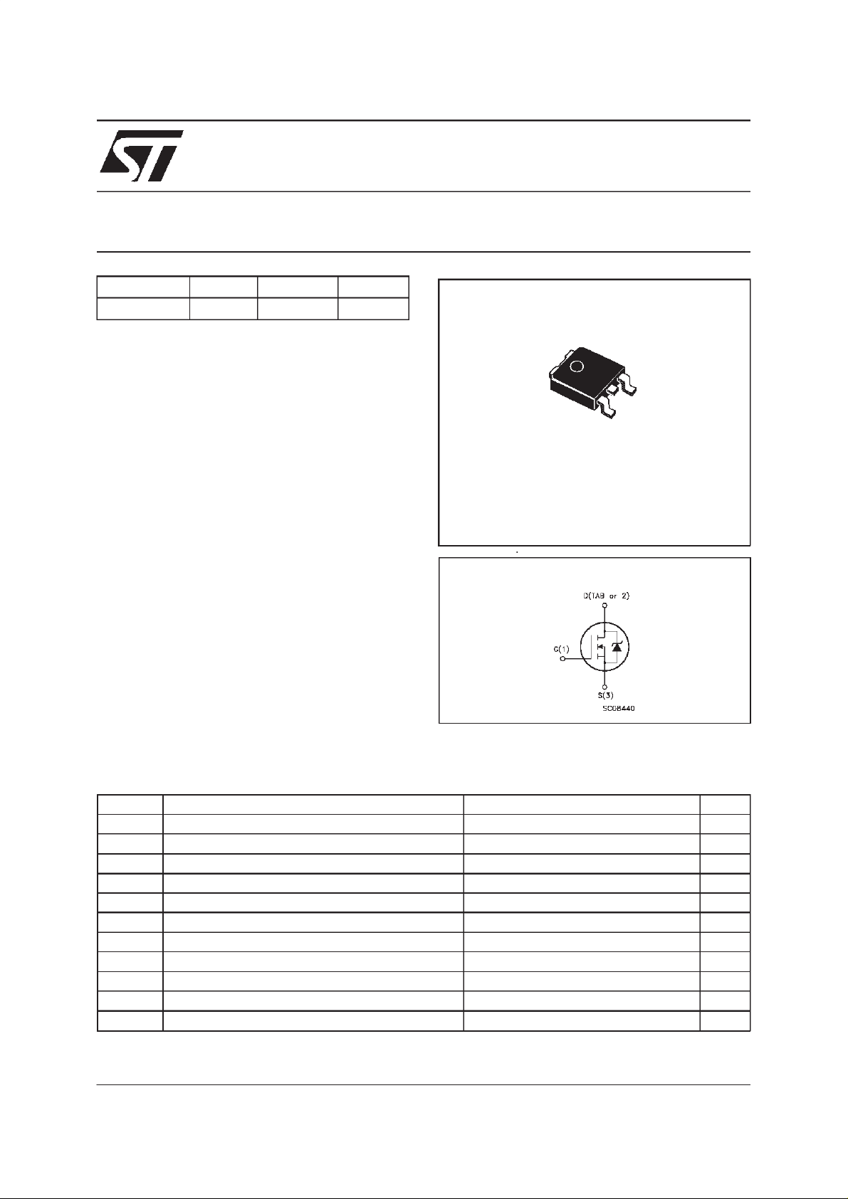
1
DPAK
TO-252
(Suffix ”T4”)
INTERNAL SCHEMATIC DIAGRAM
ABSOLUTE MAXIMUM RATINGS
Symbol Parameter Value Uni t
V
V
V
I
DM
P
dv/dt (
T
(•) Pulse width limitedby safe operatingarea (1)ISD≤30A, di/dt ≤ 300 A/µs, VDD≤ V
May 1999
Dra in- sour c e Volta ge (VGS=0) 60 V
DS
Drain- gate Voltage (RGS=20kΩ)60V
DGR
Gate-s ource Volt age ± 20 V
GS
Dra in Cu rr ent (continuous) at Tc=25oC30A
I
D
Dra in Cu rr ent (continuous) at Tc= 100oC21A
I
D
(•) D ra in Cu rr ent (pulsed) 120 A
Tot al Dissi pat io n at Tc=25oC55W
tot
Der ati ng Fa c t or 0.37 W/
1) P eak Diode Rec o ve ry volt a ge slope 7 V/ ns
St orage Tem pe ra t ure -65 to 175
stg
Max. Operating Junction Tem pe ra t ure 175
T
j
,Tj≤T
(BR)DSS
JMAX
o
C
o
C
o
C
1/8
Page 2
STD30NE06L
THERMAL DATA
R
thj-pcb
R
thj-amb
R
thj-sink
T
AVALANCHE CHARACTERISTICS
Symbol Parameter Max Valu e Unit
I
AR
E
Ther mal Resistanc e Junct ion-PC Boa rd Max
Ther mal Resistanc e Junct ion-ambient Max
Ther mal Resistanc e Case-sink Ty p
Maximum Lead Temperatur e For Soldering Pu rpose
l
Avalanche Current, Repe titive or Not-Repetitive
(pulse width limited by T
Single Pul se Avalanche Ener gy
AS
(starting T
=25oC, ID=IAR,VDD=25V)
j
max)
j
2.72
100
1.5
275
30 A
100 mJ
o
C/W
o
C/W
o
C/W
o
C
ELECTRICAL CHARACTERISTICS
=25oC unless otherwisespecified)
(T
case
OFF
Symbol Parameter Test Conditions Min. Typ. Max. U nit
V
(BR)DSS
Drain-source
ID=250µAVGS=0 60 V
Break dow n Vo lt age
I
DSS
I
GSS
Zero Gate Voltage
Drain Curre nt (V
GS
Gat e- bod y Leakag e
Current (V
DS
=0)
=0)
V
=MaxRating
DS
=MaxRating Tc= 125oC
V
DS
V
=± 20 V
GS
1
10
100 nA
±
ON(∗)
Symbol Parameter Test Conditions Min. Typ. Max. U nit
V
GS(th)
R
DS(on)
I
D(on)
Gate Threshold Volt age VDS=VGSID= 250 µ A11.72.5V
Sta t ic Drain-s our c e On
Resistance
VGS=10V ID=15A
=5V ID=15A
V
GS
On State Drain Current VDS>I
D(on)xRDS(on )max
0.022
0.025
30 A
0.028
0.030ΩΩ
VGS=10V
DYNAMIC
Symbol Parameter Test Conditions Min. Typ. Max. U nit
g
(∗)Forward
fs
Tr ansc on duc tance
C
C
C
Input Capaci t ance
iss
Out put Capac itance
oss
Reverse Transfer
rss
Capacit a nc e
VDS>I
D(on)xRDS(on )maxID
= 1 5 A 15 25 S
VDS=25V f=1MHz VGS= 0 V 2370
350
90
µ
µA
pF
pF
pF
A
2/8
Page 3
STD30NE06L
ELECTRICAL CHARACTERISTICS
(continued)
SWITCHING ON
Symbol Parameter Test Conditions Min. Typ. Max. U nit
t
d(on)
Tur n-on Delay Time
Rise Time
t
r
VDD=30V ID=15A
R
=4.7
G
Ω
VGS=5V
27
10050135
(Resis t iv e Load, see fig. 3)
Q
Q
Q
Tot al Gate Charge
g
Gat e- Source Char g e
gs
Gate-Drain Charge
gd
VDD=30V ID=30A VGS=5V 31
13
13.5
41 nC
SWITCHING OFF
Symbol Parameter Test Conditions Min. Typ. Max. U nit
t
r(Voff)
t
t
Off-volt age Rise Time
Fall T ime
f
Cross-over Tim e
c
VDD=48V ID=30A
=4.7 Ω VGS=5V
R
G
(Indu ct iv e Load, see fig . 5)
20
45
72
27
60
100
SOURCEDRAIN DIODE
Symbol Parameter Test Conditions Min. Typ. Max. U nit
I
V
I
SDM
SD
Q
I
RRM
SD
t
Source-drain Current
(•)
Source-drain Current
30
120
(pulsed)
(∗)ForwardOnVoltage ISD=30A VGS=0 1.5 V
Reverse Recovery
rr
Time
Reverse Recovery
rr
ISD= 30 A di/dt = 100 A/µs
=30V Tj=150oC
V
DD
(see test circuit, fig. 5)
55
0.1
Charge
Reverse Recovery
3.5
Current
ns
ns
nC
nC
ns
ns
ns
A
A
ns
µ
A
C
(∗) Pulsed:Pulse duration = 300µs, duty cycle 1.5%
(•) Pulse width limited by safeoperating area
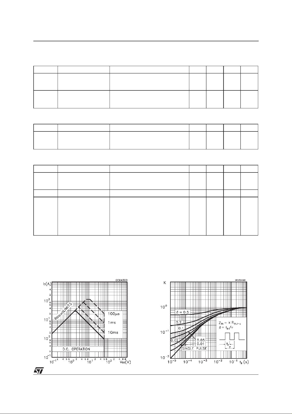
SafeOperating Area ThermalImpedance
3/8
Page 4

STD30NE06L
OutputCharacteristics
Transconductance
TransferCharacteristics
Static Drain-sourceOn Resistance
Gate Charge vs Gate-sourceVoltage
4/8
CapacitanceVariations
Page 5

STD30NE06L
NormalizedGate ThresholdVoltage vs
Temperature
Source-drainDiode Forward Characteristics
NormalizedOn Resistancevs Temperature
5/8
Page 6

STD30NE06L
Fig. 1:
UnclampedInductiveLoad TestCircuit
Fig. 3: SwitchingTimes Test Circuits For
ResistiveLoad
Fig. 2:
UnclampedInductiveWaveform
Fig. 4: Gate Charge test Circuit
Fig. 5:
Test Circuit For InductiveLoad Switching
And Diode Recovery Times
6/8
Page 7

TO-252 (DPAK) MECHANICALDATA
STD30NE06L
DIM.
mm inch
MIN. TYP. MAX. MIN. TYP. MAX.
A 2.2 2.4 0.086 0.094
A1 0.9 1.1 0.035 0.043
A2 0.03 0.23 0.001 0.009
B 0.64 0.9 0.025 0.035
B2 5.2 5.4 0.204 0.212
C 0.45 0.6 0.017 0.023
C2 0.48 0.6 0.019 0.023
D 6 6.2 0.236 0.244
E 6.4 6.6 0.252 0.260
G 4.4 4.6 0.173 0.181
H 9.35 10.1 0.368 0.397
L2 0.8 0.031
L4 0.6 1 0.023 0.039
H
A
E
C2
L2
B2
==
==
DETAIL”A”
D
2
13
L4
A1
C
A2
DETAIL”A”
B
G
==
0068772-B
7/8
Page 8

STD30NE06L
Information furnished is believed tobeaccurateand reliable. However, STMicroelectronics assumesno responsibility for the consequences
of use of such information nor for any infringement of patents or other rights of third parties which may resultfrom its use. No license is
granted by implication or otherwise under any patent or patent rights of STMicroelectronics. Specificationmentioned in this publicationare
subjecttochange without notice.Thispublication supersedesand replacesall information previouslysupplied.STMicroelectronics products
are not authorizedfor useas critical components in lifesupport devices or systems without express written approval of STMicroelectronics.
The STlogo is a trademark of STMicroelectronics
1999 STMicroelectronics – Printed in Italy – All Rights Reserved
STMicroelectronics GROUP OF COMPANIES
Australia - Brazil - Canada - China -France - Germany - Italy- Japan- Korea- Malaysia - Malta - Mexico - Morocco - The Netherlands -
8/8
Singapore - Spain - Sweden - Switzerland - Taiwan- Thailand - UnitedKingdom - U.S.A.
http://www.st.com
.
 Loading...