

Page 1
®
N - CHANNEL 60V - 0.025 Ω - 30A - DPAK
STripFET " POWER MOSFET
TYPE V
DSS
STD30NE06 60 V < 0.03 Ω 30 A
■ TYPICAL R
■ EXCEPT ION AL dv/dt CAP AB ILI T Y
■ 100% AVALANCHE TESTED
■ LOW GATE CHARGE 100
■ APPLI CATION ORIENTED
DS(on)
= 0.025 Ω
CHARACTERIZATION
■ FOR TAPE & REEL AND OTHER
PACKAGING OPTIONS CONTACT SALES
OFFICES
DESCRIPTION
This Power Mosfet is the latest development of
SGS-THOMSON unique "Single Feature Size"
strip-based process. The resulting transistor
shows extremely high packing density for low onresistance, rugged avalance characteristics and
less critical alignment steps therefore a remarkable manufacturing reproducibility.
o
R
C
DS(on)
I
D
STD30NE06
PRELIMINARY DATA
3
1
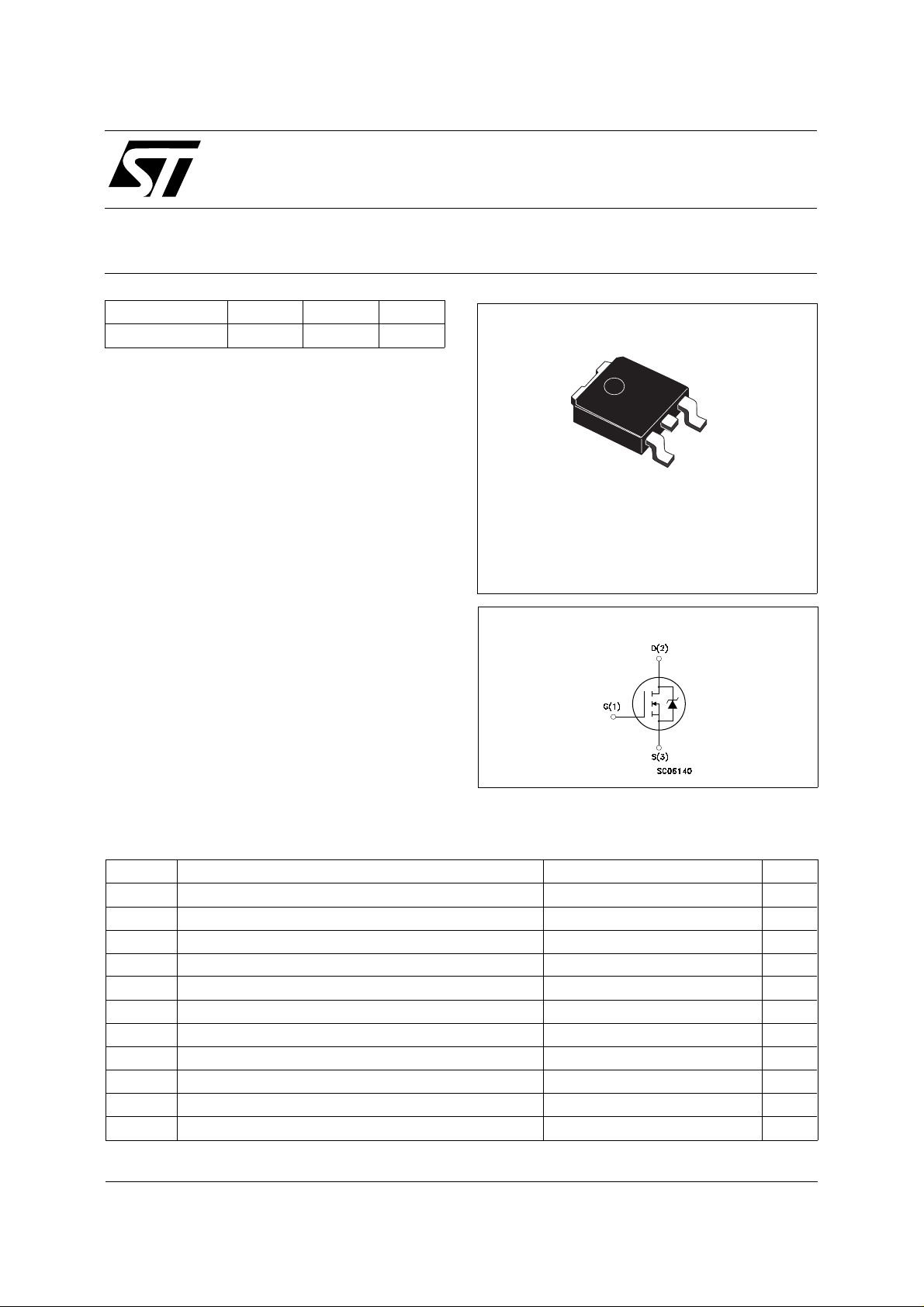
DPAK
TO-252
(Suffix "T4")
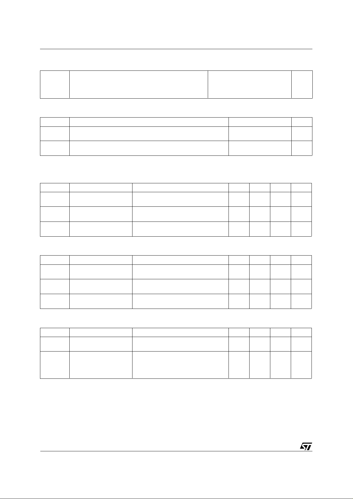
INTER NAL SCH E M ATI C DIAG RA M
APPLICATIONS
■ HIGH CURRENT, HIGH SPE ED SWI TCHING
■ SOLENOID AND RELAY DRIVER S
■ MOTOR CONT RO L, AUDIO AM PLIFI ER S
■ DC-DC & DC-AC CONVERT E RS
ABSOLUTE MAXIMUM RATINGS
Symbol Parameter Value Unit
V
V
V
I
DM
P
dv/dt Peak Diode Recovery voltage slope 7 V/ns
T
(•) Pulse width limited by safe operating area (1) ISD ≤20 A, di/dt ≤ 300 A/µs, VDD ≤ V
July 1998
Drain-source Voltage (VGS = 0) 60 V
DS
Drain- gate Voltage (RGS = 20 kΩ)
DGR
Gate-source Voltage ± 20 V
GS
I
Drain Current (continuous) at Tc = 25 oC30A
D
I
Drain Current (continuous) at Tc = 100 oC21A
D
60 V
(•) Drain Current (pulsed) 120 A
Total Dissipation at Tc = 25 oC55W
tot
Derating Factor 0.37 W/oC
Storage Temperature -65 to 175
stg
T
Max. Operating Junction Temperature 175
j
, Tj ≤ T
(BR)DSS
JMAX
o
C
o
C
1/5
Page 2
STD30NE06
THERMAL DATA
R
thj-case
Rthj-amb
R
thc-si n k
T
Thermal Resistance Junction-case Max
Thermal Resistance Junction-ambient Max
Thermal Resistance Case-sink Typ
Maximum Lead Temperature For Soldering Purpose
l
AVALANCHE CHARACTERI S TICS
Symbol Parameter Max Value Unit
I
AR
E
Avalanche Current, Repetitive or Not-Repetitive
(pulse width limited by T
Single Pulse Avalanche Energy
AS
(starting T
= 25 oC, ID = IAR, V
j
ma x)
j
DD
= 25 V)
2.72
100
1.5
275
30 A
100 mJ
o
C/W
oC/W
o
C/W
o
C
ELECTRICAL CHARACTERISTICS (T
= 25 oC unless otherwise specified)
case
OFF
Symbol Parameter Test Conditions Min. Typ. Max. Unit
V
(BR)DSS
Drain-source
I
= 250 µA V
D
GS
= 0
60 V
Breakdown Voltage
I
DSS
I
GSS
Zero Gate Voltage
Drain Current (V
GS
Gate-body Leakage
Current (V
DS
= 0)
= 0)
= Max Rating
V
DS
V
= Max Rating Tc =125 oC
DS
V
= ± 20 V
GS
1
10
± 100 nA
ON (∗)
Symbol Parameter Test Conditions Min. Typ. Max. Unit
V
GS(th)
Gate Threshold
V
= VGS ID = 250 µA
DS
234V
Voltage
R
DS(on)
Static Drain-source On
VGS = 10V ID = 15 A 0.025 0.030 Ω
Resistance
I
D(on)
On State Drain Current VDS > I
V
= 10 V
GS
D(on)
x R
DS(on)max
30 A
DYNAMIC
Symbol Parameter Test Conditions Min. Typ. Max. Unit
g
(∗) Forward
fs
Transconductance
C
C
C
Input Capacitance
iss
Output Capacitance
oss
Reverse Transfer
rss
Capacitance
VDS > I
V
DS
x R
D(on)
DS(on)max
= 25 V f = 1 MHz V
ID =15 A 15 25 S
68
3500
450
90
= 0 2700
GS
330
µA
µA
pF
pF
pF
2/5
Page 3

STD30NE06
ELECTRICAL CHARACTERISTICS (continued)
SWITCHING O N
Symbol Parameter Test Conditions Min. Typ. Max. Unit
t
d(on)
t
r
Turn-on Time
Rise Time
V
= 30 V ID = 22 A
DD
RG =4.7 Ω VGS = 10 V
27
10050135
ns
ns
Q
Q
Q
Total Gate Charge
g
Gate-Source Charge
gs
Gate-Drain Charge
gd
V
=48V ID = 45 A V
DD
= 10 V 60
GS
18
17
80 nC
SWITCHING O F F
Symbol Parameter Test Conditions Min. Typ. Max. Unit
t
r(Voff)
t
t
Off-voltage Rise Time
Fall Time
f
Cross-over Time
c
V
= 48 V ID = 45 A
DD
=4.7 Ω VGS = 10 V
R
G
20
45
72
27
60
100
SOURCE DRAIN DIO DE
Symbol Parameter Test Conditions Min. Typ. Max. Unit
30
120
I
SDM
I
SD
Source-drain Current
(•)
Source-drain Current
(pulsed)
V
(∗) Forward On Voltage ISD = 45 A VGS = 0 1.5 V
SD
t
Q
Reverse Recovery
rr
Time
Reverse Recovery
rr
I
= 45 A di/dt = 100 A/µs
SD
V
= 30 V Tj = 150 oC
DD
70
210
Charge
I
RRM
Reverse Recovery
6
Current
(∗) Pulsed: Pulse duration = 300 µs, duty cycle 1.5 %
(•) Pulse width limited by safe operating area
nC
nC
ns
ns
ns
A
A
ns
µC
A
3/5
Page 4

STD30NE06
TO-252 (DPAK) MECHANICAL DATA
DIM.
mm inch
MIN. TYP. MAX. MIN. TYP. MAX.
A 2.2 2.4 0.086 0.094
A1 0.9 1.1 0.035 0.043
A2 0.03 0.23 0.001 0.009
B 0.64 0.9 0.025 0.035
B2 5.2 5.4 0.204 0.212
C 0.45 0.6 0.017 0.023
C2 0.48 0.6 0.019 0.023
D 6 6.2 0.236 0.244
E 6.4 6.6 0.252 0.260
G 4.4 4.6 0.173 0.181
H 9.35 10.1 0.368 0.397
L2 0.8 0.031
L4 0.6 1 0.023 0.039
4/5
A
C2
L2
E
B2
==
H
DETAIL "A"
D
==
C
B
2
1 3
L4
A1
G
==
A2
DETAIL "A"
0068772-B
Page 5

STD30NE06
Information furnished is believed to be accurate and reliable. However, STMicroelectronics assumes no responsibility for the consequences
of use of such information n or for any infrin gement of patents or othe r rights of third parties which may result from its use. No licens e i s
granted by implication or otherwise under any patent or patent rights of STMicroelectronics. Specification mentioned in this publication are
subject to change without notice. This publication supersedes and replaces all information previously supplied. STMicroelectronics products
are not authorized for use as critical components in life support devices or systems without express written approval of STMicroelectronics.
Australia - Brazil - Canada - China - France - Germany - Italy - Japan - Korea - Malaysia - Malta - Mexico - Morocco - The Netherlands -
Singapore - Spain - Sweden - Switzerland - Taiwan - Thailand - United Kingdom - U.S.A.
The ST logo is a trademark of STMicroelectronics
© 1998 STMicroelectronics – Printed in Italy – All Rights Reserved
STMicroelectronics GROUP OF COMPANIES
.
5/5
 Loading...