

Page 1
STD2NC40-1
N-CHANNEL 400V - 4.7Ω - 1.5A IPAK
PowerMeshII MOSFET
TYPE V
DSS
R
DS(on)
I
D
STD2NC40-1 400V <5.5Ω 1.5A
■ TYPICAL R
■ EXTREMELY HIGH dv/dt CAPABILITY
■ 100% AVALANCHE TESTED
■ NEW HIGH VOLTAGE BENCHMARK
■ GATE CHARGE MINIMIZED
(on) = 4.7Ω
DS
DESCRIPTION
The PowerMESHII is the evolution of the first
generation of MESH OVERLAY. The layout refinements introduced greatly improve the Ron*area
figure of merit while keeping the device at the leading edge for what concerns swithing speed, gate
charge and ruggedness.
APPLICATIONS
■ SWITH MODE LOW POWER SUPPLIES
(SMPS)
■ CFL
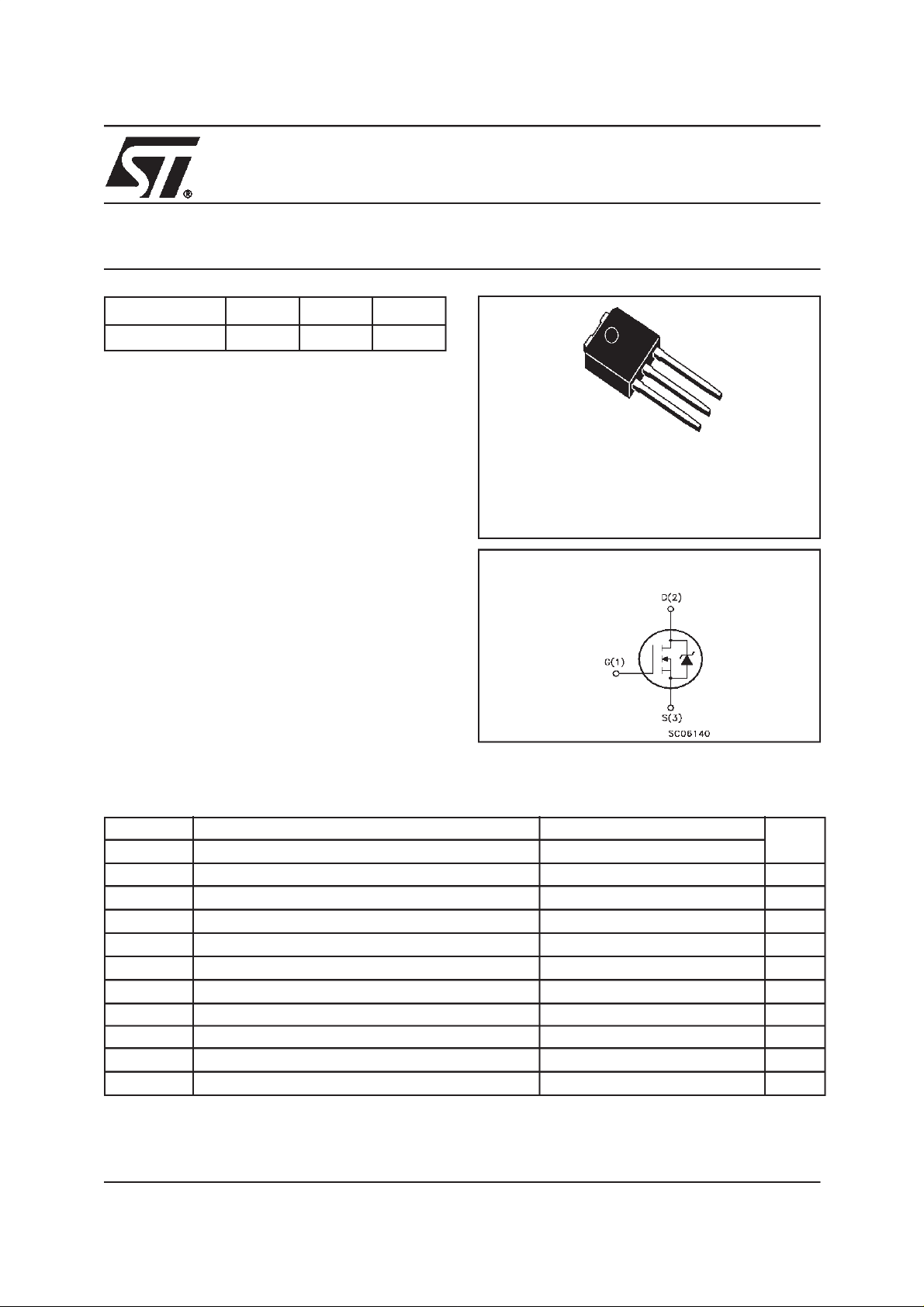
3
2
1
IPAK
(SUFFIX“-1”)
INTERNAL SCHEMATIC DIAGRAM
ABSOLUTE MAXIMUM RATINGS
Symbol Parameter Value Unit
V
DS
V
DGR
V
GS
I
D
I
D
I
DM
P
TOT
dv/dt Peak Diode Recovery voltage slope 3.5 V/ns
T
stg
T
j
(•)Pulse width limited by safe operating area
This is preliminary information on a new product now in development or undergoing evaluation. Details are subject to change without notice.
Drain-source Voltage (VGS=0)
Drain-gate Voltage (RGS=20kΩ)
400 V
400 V
Gate- source Voltage ±30 V
Drain Current (continuos) at TC=25°C
Drain Current (continuos) at TC= 100°C
(■)
Drain Current (pulsed) 6 A
TotalDissipation at TC=25°C
1.5 A
0.95 A
30 W
Derating Factor 0.24 W/°C
Storage Temperature –60 to 150 °C
Max. Operating Junction Temperature 150 °C
(1)ISD≤1.5A, di/dt ≤100A/µs, VDD≤ V
(BR)DSS,Tj≤TJMAX.
1/8May 2000
Page 2
STD2NC40-1
THERMAL DATA
Rthj-case Thermal Resistance Junction-case Max 4.16 °C/W
Rthj-amb Thermal Resistance Junction-ambient Max 100 °C/W
Rthc-sink Thermal Resistance Case-sink Typ 1.5 °C/W
T
l
AVALANCHE CHARACTERISTICS
Symbol Parameter Max Value Unit
I
AR
E
AS
ELECTRICAL CHARACTERISTICS (TCASE = 25 °C UNLESS OTHERWISE SPECIFIED)
OFF
Symbol Parameter Test Conditions Min. Typ. Max. Unit
V
(BR)DSS
I
DSS
I
GSS
Maximum Lead Temperature For Soldering Purpose 275 °C
Avalanche Current, Repetitive or Not-Repetitive
(pulse width limited by T
max)
j
Single Pulse Avalanche Energy
(starting T
Drain-source
Breakdown Voltage
Zero Gate Voltage
Drain Current (V
Gate-body Leakage
Current (V
=25°C, ID=IAR,VDD=50V)
j
I
= 250 µA, VGS=0
D
= Max Rating
V
DS
=0)
DS
GS
=0)
V
= Max Rating, TC= 125 °C
DS
= ±30V
V
GS
400 V
1.5 A
125 mJ
1 µA
50 µA
±100 nA
ON (1)
Symbol Parameter Test Conditions Min. Typ. Max. Unit
V
GS(th)
R
DS(on)
I
D(on)
Gate Threshold Voltage
Static Drain-source On
Resistance
On State Drain Current
V
DS=VGS,ID
= 10V,ID= 0.7 A
V
GS
V
DS>ID(on)xRDS(on)max,
= 250µA
VGS=10V
234V
4.7 5.5 Ω
1.5 A
DYNAMIC
Symbol Parameter Test Conditions Min. Typ. Max. Unit
V
g
(1)
fs
C
iss
C
oss
C
rss
Forward Transconductance
Input Capacitance
Output Capacitance 22.5 pF
Reverse Transfer
Capacitance
DS>ID(on)xRDS(on)max,
ID=0.7A
V
= 25V, f = 1 MHz, VGS=0
DS
1.1 S
108 pF
0.4 pF
2/8
Page 3
STD2NC40-1
ELECTRICAL CHARACTERISTICS (CONTINUED)
SWITCHING ON
Symbol Parameter Test Conditions Min. Typ. Max. Unit
t
d(on)
Q
Q
Q
t
r
g
gs
gd
Turn-on Delay Time
Rise Time 12 ns
TotalGate Charge
Gate-Source Charge 2.1 nC
Gate-Drain Charge 2.4 nC
SWITCHING OFF
Symbol Parameter Test Conditions Min. Typ. Max. Unit
t
r(Voff)
t
t
f
c
Off-voltage Rise Time
Fall Time 27 ns
Cross-over Time 29 ns
V
= 200V,ID= 0.7A
DD
= 4.7Ω VGS= 10V
R
G
(see test circuit, Figure 3)
V
= 320V,ID = 1.5A,
DD
= 10V
V
GS
V
= 320V,ID= 1.5A,
DD
=4.7Ω, VGS= 10V
R
G
(see test circuit, Figure 5)
7.5 ns
6.1 8.2 nC
20 ns
SOURCE DRAIN DIODE
Symbol Parameter Test Conditions Min. Typ. Max. Unit
I
SDM
V
SD
I
SD
t
rr
Source-drain Current 1.5 A
(1)
Source-drain Current (pulsed) 6 A
(2)
Forward On Voltage
Reverse Recovery Time
ISD= 1.5A, VGS=0
I
= 1.5A, di/dt = 100A/µs,
SD
= 100V,Tj= 150°C
V
DD
180 ns
1.5 V
(see test circuit, Figure 5)
Q
rr
I
RRM
Note: 1. Pulsed: Pulse duration = 300 µs, duty cycle 1.5 %.
2. Pulse width limited by safe operating area.
Reverse Recovery Charge 625 nC
Reverse Recovery Current 5 A
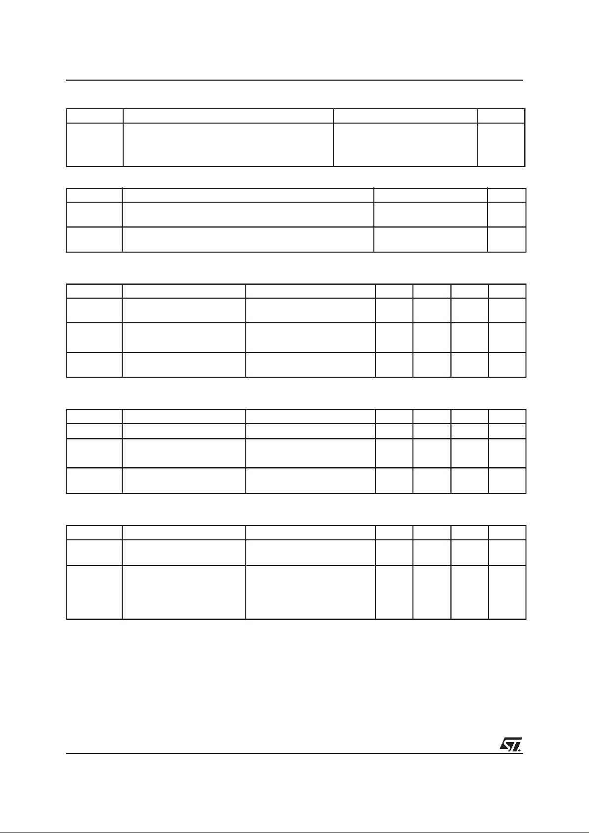
Thermal ImpedenceSafe Operating Area
3/8
Page 4
STD2NC40-1
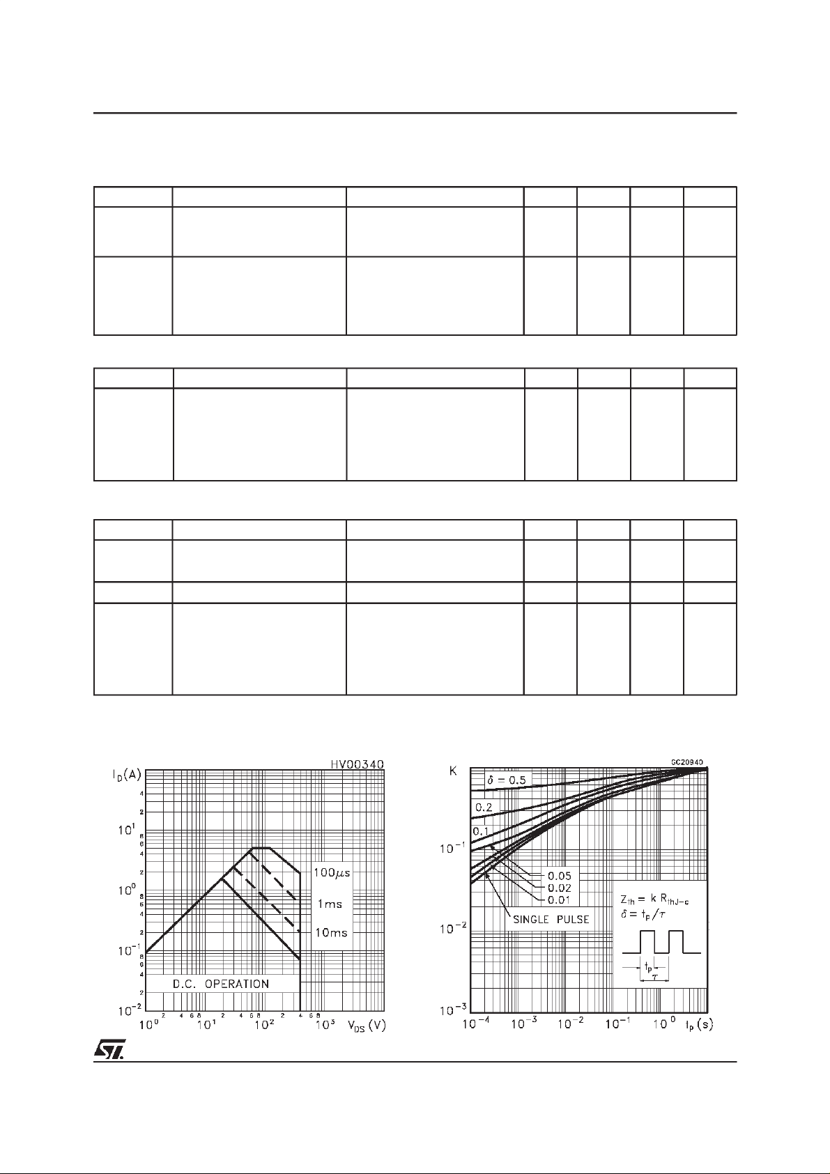
Output Characteristics
Transconductance
Transfer Characteristics
Static Drain-source On Resistance
Gate Charge vs Gate-source Voltage
4/8
Capacitance Variations
Page 5

STD2NC40-1
Normalized Gate Threshold Voltage vs
Temperature
Source-drain Diode Forward Characteristics
Normalized On Resistance vs Temperature
5/8
Page 6
STD2NC40-1
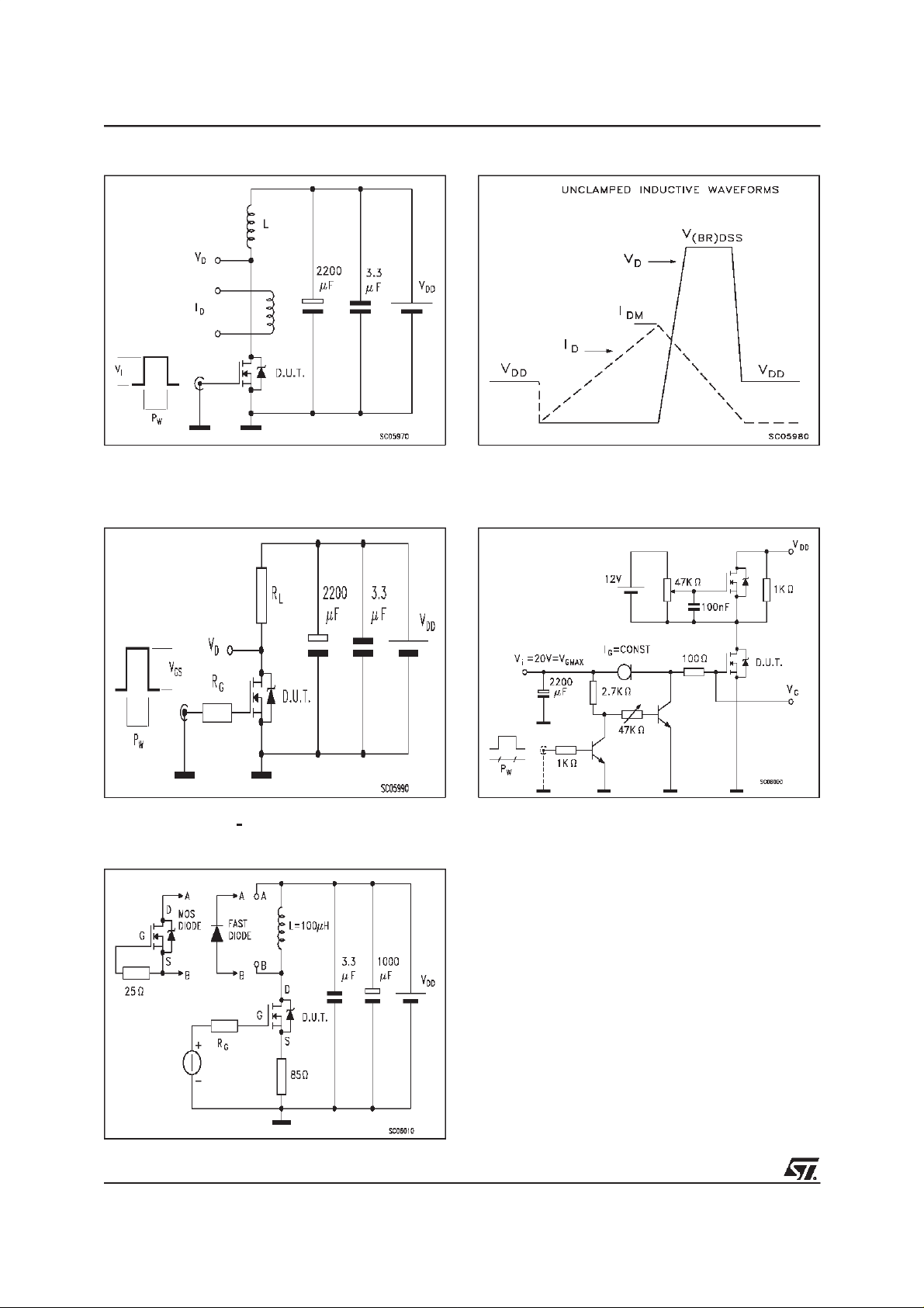
Fig. 2: Unclamped Inductive WaveformFig. 1: Unclamped Inductive Load Test Circuit
Fig. 3: Switching Times Test Circuit For
Resistive Load
Fig. 5: Test Circuit For Inductive Load Switching
And Diode Recovery Times
Fig. 4: Gate Charge test Circuit
6/8
Page 7
TO-251 (IPAK) MECHANICAL DATA
STD2NC40-1
DIM.
MIN. TYP. MAX. MIN. TYP. MAX.
mm inch
A 2.2 2.4 0.086 0.094
A1 0.9 1.1 0.035 0.043
A3 0.7 1.3 0.027 0.051
B 0.64 0.9 0.025 0.031
B2 5.2 5.4 0.204 0.212
B3 0.85 0.033
B5 0.3 0.012
B6 0.95 0.037
C 0.45 0.6 0.017 0.023
C2 0.48 0.6 0.019 0.023
D 6 6.2 0.236 0.244
E 6.4 6.6 0.252 0.260
G 4.4 4.6 0.173 0.181
H 15.9 16.3 0.626 0.641
L 9 9.4 0.354 0.370
L1 0.8 1.2 0.031 0.047
L2 0.8 1 0.031 0.039
H
A
E
==
C2
L2
B2
==
D
B3
2
13
L1
B6
A1
C
A3
L
B
B5
G
==
0068771-E
7/8
Page 8

STD2NC40-1
8/8
Information furnished is believed to beaccurate and reliable. However, STMicroelectronics assumes no responsibility for theconsequences
of use of such information nor for any infringement of patents or other rights of third parties which may result from its use. No license is
granted by implication or otherwise under any patent or patent rights of STMicroelectronics. Specification mentioned in this publication are
subject tochange withoutnotice. This publication supersedes and replaces all information previously supplied. STMicroelectronics products
are not authorized for use as critical components in life support devices or systems withoutexpress written approval of STMicroelectronics.
Australia - Brazil - China - Finland- France- Germany - Hong Kong - India- Italy- Japan - Malaysia -Malta - Morocco -
The ST logois a trademark of STMicroelectronics
2000 STMicroelectronics – Printed in Italy– AllRights Reserved
STMicroelectronicsGROUP OF COMPANIES
Singapore - Spain -Sweden - Switzerland - United Kingdom - U.S.A.
http://www.st.com
 Loading...