

Page 1
STD2NC50
STD2NC50-1
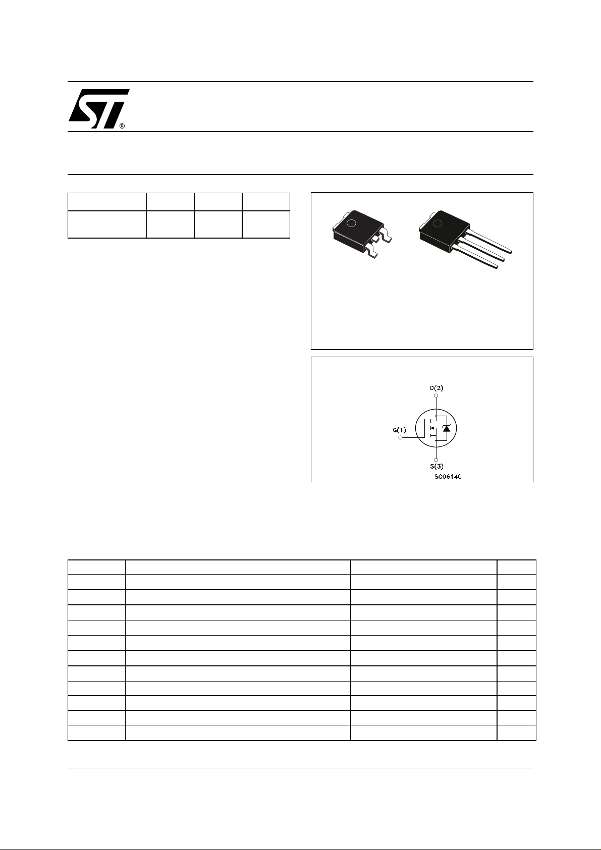
N-CHANNEL 500V - 3Ω - 2.2A DPAK/IPAK
PowerMesh™II MOSFET
TYPE V
STD2NC50
STD2NC50-1
■ TYPICAL R
■ EXTREMELY HIGH dv /d t C APABILITY
■ 100% AVALANCHE TESTED
■ NEW HIGH VOLTAGE BENCHMARK
■ GATE CHARGE MINIMIZED
DS
DSS
500 V
500 V
(on) = 3 Ω
R
DS(on)
< 4
< 4
I
D
Ω
Ω
2.2 A
2.2 A
DESCRIPTION
The PowerMESH
generation of MESH OVERLAY
™II is the evolution of the first
™. The layout re-
finements introduced greatly improve the Ron*area
figure of merit while keeping the device at the lea ding edge for what concerns swithing speed, gate
charge and ruggedness.
APPLICATIONS
■ HIGH CURRENT, HIGH SPEED SWITCHING
■ SWITH MODE POWER SUPPLI ES ( SMPS)
■ DC-AC CONVERTERS FOR WELDING
EQUIPMENT AND UNINTERRUPTIBLE
POWER SUPPLIES AND MOTOR DRIVER
3
1
DPAK
IPAK
INTERNAL SCHEMATIC DIAGRAM
3
2
1
ABSOLUTE MAXIMUM RATINGS
Symbol Parameter Value Unit
(1)
j
Drain-source Voltage (VGS = 0)
Drain-gate Voltage (RGS = 20 kΩ)
Gate- source Voltage ±30 V
Drain Current (continuos) at TC = 25°C
Drain Current (continuos) at TC = 100°C
Drain Current (pulsed) 8.8 A
Total Dissipation at TC = 25°C
Derating Factor 0.36 W/°C
Storage Temperature –60 to 150 °C
Max. Operating Junction Temperature 150 °C
(1)ISD ≤ 2.2A, di/dt ≤100A/µs, VDD ≤ V
500 V
500 V
2.2 A
1.4 A
45 W
, Tj ≤ T
(BR)DSS
JMAX
V
DS
V
DGR
V
GS
I
D
I
D
I
DM
P
TOT
dv/dt Peak Diode Recovery voltage slope 3 V/ns
T
stg
T
(•)Pu l se width limite d by safe operat i ng area
1/10May 2001
Page 2
STD2NC50 / STD2NC50-1
THERMA L D ATA
Rthj-case Thermal Resistance Junction-case Max 2.78 °C/W
Rthj-amb Thermal Resistance Junction-ambient Max 62.5 °C/W
T
AVALANCHE CHARACTERISTICS
Symbol Parameter Max Value Unit
I
AR
E
AS
ELECTRICAL CHARACTERISTICS (TCASE = 25 °C UNLESS OTHERWISE SPECIFIED)
OFF
Symbol Parameter Test Conditions Min. Typ. Max. Unit
V
(BR)DSS
I
DSS
I
GSS
Maximum Lead Temperature For Soldering Purpose 300 °C
l
Avalanche Current, Repetitive or Not-Repetitive
(pulse width limited by T
max)
j
Single Pulse Avalanche Energy
(starting T
= 25 °C, ID = IAR, VDD = 50 V)
j
Drain-source
Breakdown Voltage
Zero Gate Voltage
Drain Current (V
GS
= 0)
Gate-body Leakage
Current (V
DS
= 0)
2.2 A
140 mJ
ID = 250 µA, VGS = 0 500
V
= Max Rating
DS
V
= Max Rating, TC = 125 °C
DS
V
= ±30V ±100 nA
GS
1µA
50 µA
V
ON
(1)
Symbol Parameter Test Conditions Min. Typ. Max. Unit
V
GS(th)
R
DS(on)
Gate Threshold Voltage
Static Drain-source On
V
= VGS, ID = 250µA
DS
VGS = 10V, ID = 1.4 A
234V
34
Resistance
DYNAMIC
Symbol Parameter Test Conditions Min. Typ. Max. Unit
(1) Forward Transconductance VDS > I
g
fs
C
iss
C
oss
C
rss
Input Capacitance
Output Capacitance 45 pF
Reverse Transfer
Capacitance
I
D
V
= 1.4A
DS
D(on)
x R
DS(on)max,
= 25V, f = 1 MHz, VGS = 0
2S
260 pF
5pF
Ω
2/10
Page 3
STD2NC50 / STD2NC50-1
ELECTRICAL CHARACTERISTICS (CONTINUED)
SWITCHING ON
Symbol Parameter Test Conditions Min. Typ. Max. Unit
t
d(on)
Turn-on Delay Time
t
r
Rise Time
= 250V, ID = 1.4 A
V
DD
RG= 4.7Ω VGS = 10V
(see test circuit, Figure 3)
Q
g
Q
gs
Q
gd
Total Gate Charge
Gate-Source Charge
Gate-Drain Charge
= 400V, ID = 2.8 A,
V
DD
VGS = 10V
SWITCHING OFF
Symbol Parameter Test Conditions Min. Typ. Max. Unit
= 400V, ID = 2.8 A,
t
r(Voff)
t
t
Off-voltage Rise Time
f
c
Fall Time
Cross-over Time
V
DD
RG=4.7Ω, V
GS
= 10V
(see test circuit, Figure 5)
SOURCE DRAIN DIODE
Symbol Parameter Test Conditions Min. Typ. Max. Unit
I
SD
I
SDM
VSD (1)
t
rr
Q
rr
I
RRM
Note: 1. Pulsed: Pu l se duration = 300 µs, duty cycle 1.5 %.
2. Pulse width li mited by safe operating area .
Source-drain Current 2.2 A
(2)
Source-drain Current (pulsed) 8.8 A
Forward On Voltage
Reverse Recovery Time
Reverse Recovery Charge 2200 nC
ISD = 2.2 A, VGS = 0
I
= 2.8A, di/dt = 100A/µs,
SD
V
= 100V, Tj = 150°C
DD
(see test circuit, Figure 5)
Reverse Recovery Current 11.5 A
10
10
10
13.5 nC
2.5
4.5
10
8
20
1.6 V
380 ns
ns
ns
nC
nC
ns
ns
ns
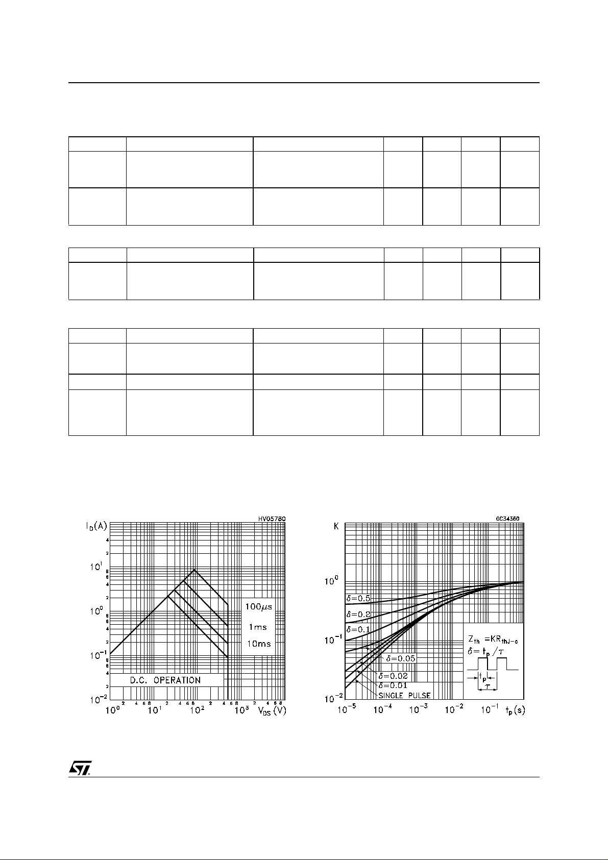
Safe Operating Area Thermal Impedence
3/10
Page 4

STD2NC50 / STD2NC50-1
Output Characteristics
Transfer Characteristics
Static Drain-source On ResistanceTransconductance
Gate Charge vs Gate-source Voltage
4/10
Capacitance Variations
Page 5
STD2NC50 / STD2NC50-1
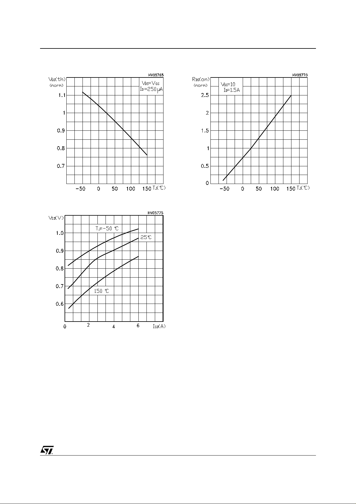
Normalized Gate Threshold Voltage vs
Temperature
Source-drain Diode Forw ard Ch aracteristi cs
Normalized On Resistance vs Temperatur e
5/10
Page 6

STD2NC50 / STD2NC50-1
Fig. 2: Unclamped Inductive WaveformFig. 1: Unclamped Inductive Load Test Circuit
Fig. 3: Switching Times Test Circuit For
Resistive Load
Fig. 5: Test Circuit For Inductive Load Switching
And Diode Recovery Times
Fig. 4: Gate Charge test Circuit
6/10
Page 7

TO-252 (DPAK) MECHANICAL DATA
STD2NC50 / STD2NC50-1
DIM.
A 2.20 2.40 0.087 0.094
A1 0.90 1.10 0.035 0.043
A2 0.03 0.23 0.001 0.009
B 0.64 0.90 0.025 0.035
B2 5.20 5.40 0.204 0.213
C 0.45 0.60 0.018 0.024
C2 0.48 0.60 0.019 0.024
D 6.00 6.20 0.236 0.244
E 6.40 6.60 0.252 0.260
G 4.40 4.60 0.173 0.181
H 9.35 10.10 0.368 0.398
L2 0.8 0.031
L4 0.60 1.00 0.024 0.039
V2 0
MIN. TYP. MAX. MIN. TYP. MAX.
o
mm inch
o
8
o
0
o
0
P032P_B
7/10
Page 8

STD2NC50 / STD2NC50-1
TO-251 (IPAK) MECHANICAL DAT A
DIM.
MIN. TYP. MAX. MIN. TYP. MAX.
mm inch
A 2.2 2.4 0.086 0.094
A1 0.9 1.1 0.035 0.043
A3 0.7 1.3 0.027 0.051
B 0.64 0.9 0.025 0.031
B2 5.2 5.4 0.204 0.212
B3 0.85 0.033
B5 0.3 0.012
B6 0.95 0.037
C 0.45 0.6 0.017 0.023
C2 0.48 0.6 0.019 0.023
D 6 6.2 0.236 0.244
E 6.4 6.6 0.252 0.260
G 4.4 4.6 0.173 0.181
H 15.9 16.3 0.626 0.641
L 9 9.4 0.354 0.370
L1 0.8 1.2 0.031 0.047
L2 0.8 1 0.031 0.039
H
8/10
A
C2
L2
E
B2
= =
= =
D
B3
2
1 3
L1
A1
L
B6
C
A3
B
B5
G
= =
0068771-E
Page 9

STD2NC50 / STD2NC50-1
DPAK FOOTPRINT
All dimensions are in millimeters
TAPE AND REEL SHIPMENT (suffix ”T4”)*
TUBE SHIPMENT (no suffix)*
All dimensions
are in millimeters
REEL MECHANICAL DATA
DIM.
A 330 12.992
B 1.5 0.059
C 12.8 13.2 0.504 0.520
D 20.2 0.795
G 16.4 18.4 0.645 0.724
N 50 1.968
T 22.4 0.881
mm inch
MIN. MAX. MIN. MAX.
TAPE MECHANICAL DATA
DIM.
A0 6.8 7 0.267 0.275
B0 10.4 10.6 0.409 0.417
B1 12.1 0.476
D 1.5 1.6 0.059 0.063
D1 1.5 0.059
E 1.65 1.85 0.065 0.073
F 7.4 7.6 0.291 0.299
K0 2.55 2.75 0.100 0.108
P0 3.9 4.1 0.153 0.161
P1 7.9 8.1 0.311 0.319
P2 1.9 2.1 0.075 0.082
R 40 1.574
W 15.7 16.3 0.618 0.641
* on s ales type
9/10
mm inch
MIN. MAX. MIN. MAX.
BASE QTY BULK QTY
2500 2500
Page 10

STD2NC50 / STD2NC50-1
Information furnished is believed to be accurate and reliable. However, STMicroelectronics assumes no responsibility for the consequences
of use of such informa tion n or for an y infring ement of patent s or other rig hts of third part ies which may resu lt from its use . No l i cen se i s
granted by implication or otherwise under any patent or patent rights of STMicroelectronics. Specification mentioned in this publication are
subject to change without notice. This publication supersedes and replaces all information previously supplied. STMicroelectronics products
are not authorized for use as critical compo nents in life support devices or systems without express written approval of STMicroelectronics.
Australia - Brazil - China - Finland - France - Germany - Hong Kong - India - Italy - Japan - Malaysia - Malta - Morocco -
The ST logo is a trademark of STMicroelectronics
© 2001 STMicroelectronics – Printed in Italy – All Rights Reserved
STMicroelectronics GROUP OF COMPANIES
Singapore - Spain - Sweden - Switzerland - United Kingdom - U.S.A.
http://www.st.com
10/10
 Loading...