

Page 1
STD2NB80
N - CHANNEL 800V - 4.6
TYPE V
ST D2N B 80 80 0 V < 6.5 Ω 1.9 A
■ TYPICALR
■ EXTREMELYHIGH dv/dtCAPABILITY
■ 100%AVALANCHETESTED
■ VERYLOW INTRINSIC CAPACITANCES
■ GATECHARGE MINIMIZED
■ ADDSUFFIX ”T4” FORORDERING INTAPE
DS(on)
DSS
= 4.6 Ω
& REEL(2500UNITS)
DESCRIPTION
Using the latesthigh voltage MESH OVERLAY
process, STMicroelectronics has designed an
advanced family of power MOSFETs with
outstanding performances. The new patent
pending strip layout coupled with the Company’s
proprietary edge termination structure, gives the
lowest R
per area, exceptional avalanche
DS(on)
and dv/dt capabilities and unrivalled gate charge
and switching characteristics.
R
DS(on)
I
D
Ω
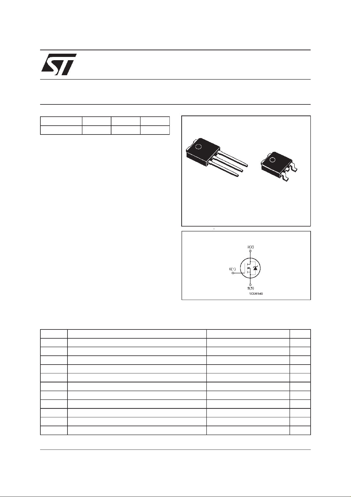
- 1.9A - IPAK/DPAK
PowerMESH MOSFET
3
2
1
IPAK
TO-251
(Suffix”-1”)
DPAK
TO-252
(Suffix ”T4”)
INTERNAL SCHEMATIC DIAGRAM
3
1
APPLICATIONS
■ SWITCHMODE POWER SUPPLIES(SMPS)
■ DC-AC CONVERTERS FOR WELDING
EQUIPMENTAND UNINTERRUPTIBLE
POWERSUPPLIESAND MOTORDRIVE
ABSOLUTE MAXIMUM RATINGS
Symbol Parameter Value Unit
V
V
V
I
DM
P
dv/ dt(
T
(•) Pulsewidth limited by safe operating area (1)ISD≤ 2A, di/dt ≤ 200A/µs, VDD≤ V
January 1999
Drain-source Voltage (VGS=0) 800 V
DS
Dra in- gat e Volt age (RGS=20kΩ)
DGR
Gate -sourc e Vo ltage ± 30 V
GS
I
Drain Current (co ntinuous) at Tc=25oC1.9A
D
I
Drain Current (co ntinuous) at Tc=100oC1.2A
D
(•) Drain Current (pulsed) 7.6 A
Total Dissipation a t Tc=25oC55W
tot
Derating Factor 0.44 W/
1) P eak Dio de Recove ry volt age slop e 4.5 V/ns
St orage T emper ature -65 t o 1 50
stg
T
Max. Op er a t ing J unctio n T emper at u r e 150
j
800 V
,Tj≤T
(BR)DSS
JMAX
o
C
o
C
o
C
1/9
Page 2
STD2NB80
THERMAL DATA
R
thj-case
Rthj-a mb
R
thc-sink
T
AVALANCHE CHARACTERISTICS
Symbol Para meter Max Val ue Uni t
I
AR
E
Ther mal Resis t an ce Junc ti on-cas e Max
Ther mal Resis t an ce Junc ti on-ambien t Max
Thermal Resistance Case-sink Typ
Maximum Lead Temperat ure For Soldering Purpose
l
Avalanche Cu rr ent, Re petitiv e or No t - Re petitive
(pulse width limited by T
Single Pulse Avalanche Energ y
AS
(starting T
=25oC, ID=IAR,VDD=50V)
j
max)
j
2.27
100
1
275
1.9 A
176 mJ
o
C/W
oC/W
o
C/W
o
C
ELECTRICAL CHARACTERISTICS (T
=25oC unless otherwisespecified)
case
OFF
Symbol Parameter Test Conditions Min. Typ. M ax. Unit
V
(BR)DSS
Drain-sourc e
=250µAVGS=0
I
D
800 V
Break d own Voltage
I
DSS
I
GSS
Zero Gate Voltage
Drain Current (V
GS
Gat e- b ody Le akage
Current (V
DS
=0)
=0)
V
=MaxRating
DS
= Max Rating Tc=125oC
V
DS
= ± 30 V
V
GS
1
50
± 100 nA
ON(∗)
Symbol Parameter Test Conditions Min. Typ. M ax. Unit
V
GS(th)
Gate Threshold
V
DS=VGSID
= 250 µA
345V
Voltage
R
DS(on)
Static Drain-source On
VGS=10V ID=1.3 A 4.6 6.5
Resistanc e
I
D(on)
On S t ate Drain Current VDS>I
D(on)xRDS(on)max
1.9 A
VGS=10V
DYNAMIC
Symbol Parameter Test Conditions Min. Typ. M ax. Unit
g
(∗)Forward
fs
Tr ansconduc tance
C
C
C
Input Capacit an c e
iss
Out put Capacita nce
oss
Reverse Transf er
rss
Capacitance
VDS>I
D(on)xRDS(on)maxID
=1.3A 1 2 S
VDS=25V f=1MHz VGS=0 440
60
7
µA
µ
Ω
pF
pF
pF
A
2/9
Page 3
STD2NB80
ELECTRICAL CHARACTERISTICS (continued)
SWITCHINGON
Symbol Parameter Test Conditions Min. Typ. M ax. Unit
t
d(on)
t
Turn-on delay Ti me
Rise Time
r
VDD= 400 V ID=1.5A
=4.7 Ω VGS=10V
R
G
(see test circu it, figure 3)
Q
Q
Q
Total Gate Charge
g
Gat e- Source Cha rge
gs
Gate-Drain Charge
gd
VDD= 640 V ID=3 A VGS=10V 17
SWITCHINGOFF
Symbol Parameter Test Conditions Min. Typ. M ax. Unit
t
r(Voff)
t
Off -voltage Rise Ti me
t
Fall Time
f
Cross-ov er T i me
c
VDD= 640 V ID=3 A
=4.7 Ω VGS=10V
R
G
(see test circu it, figure 5)
SOURCEDRAINDIODE
Symbol Parameter Test Conditions Min. Typ. M ax. Unit
I
SD
I
SDM
V
SD
t
Q
I
RRM
(∗) Pulsed: Pulse duration = 300 µs, dutycycle 1.5%
(•) Pulse width limited by safeoperating area
Source-drain Curr ent
(•)
Source-drain Curr ent
(pulsed)
(∗) F orward On Voltage ISD=1.9A VGS=0 1.6 V
Reverse Reco v er y
rr
Time
Reverse Reco v er y
rr
=2.6A di/dt=100A/µs
I
SD
= 100 V Tj=150oC
V
DD
(see test circu it, figure 5)
Charge
Reverse Reco v er y
Current
12
10
24 nC
6.5
7.5
15
17
22
1.9
7.6
650
2.8
8.5
ns
ns
nC
nC
ns
ns
ns
A
A
ns
µ
A
C
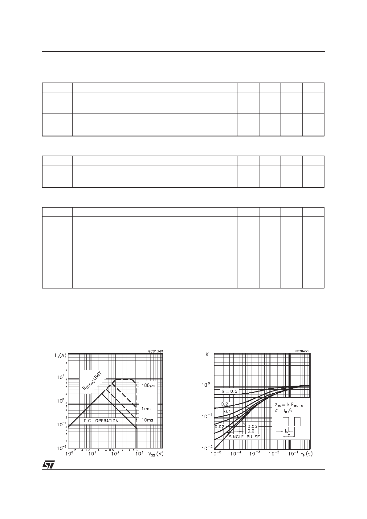
SafeOperating Area ThermalImpedance
3/9
Page 4

STD2NB80
OutputCharacteristics
Transconductance
TransferCharacteristics
Static Drain-sourceOn Resistance
Gate Charge vs Gate-sourceVoltage
4/9
CapacitanceVariations
Page 5

STD2NB80
Normalized Gate ThresholdVoltage vs
Temperature
Source-drainDiode Forward Characteristics
Normalized On Resistancevs Temperature
5/9
Page 6

STD2NB80
Fig. 1: UnclampedInductive Load Test Circuit
Fig. 3: SwitchingTimes Test CircuitsFor
ResistiveLoad
Fig. 2: UnclampedInductiveWaveform
Fig. 4: Gate Charge test Circuit
Fig. 5: Test CircuitFor InductiveLoad Switching
And Diode Recovery Times
6/9
Page 7

TO-251 (IPAK) MECHANICALDATA
STD2NB80
DIM.
mm inch
MIN. TYP. MAX. MIN. TYP. MAX.
A 2.2 2.4 0.086 0.094
A1 0.9 1.1 0.035 0.043
A3 0.7 1.3 0.027 0.051
B 0.64 0.9 0.025 0.031
B2 5.2 5.4 0.204 0.212
B3 0.85 0.033
B5 0.3 0.012
B6 0.95 0.037
C 0.45 0.6 0.017 0.023
C2 0.48 0.6 0.019 0.023
D 6 6.2 0.236 0.244
E 6.4 6.6 0.252 0.260
G 4.4 4.6 0.173 0.181
H 15.9 16.3 0.626 0.641
L 9 9.4 0.354 0.370
L1 0.8 1.2 0.031 0.047
L2 0.8 1 0.031 0.039
A
E
==
C2
L2
B2
==
H
C
A3
A1
B6
L
B
B5
G
==
D
B3
2
13
L1
0068771-E
7/9
Page 8

STD2NB80
TO-252 (DPAK) MECHANICALDATA
DIM.
mm inch
MIN. TYP. MAX. MIN. TYP. MAX.
A 2.2 2.4 0.086 0.094
A1 0.9 1.1 0.035 0.043
A2 0.03 0.23 0.001 0.009
B 0.64 0.9 0.025 0.035
B2 5.2 5.4 0.204 0.212
C 0.45 0.6 0.017 0.023
C2 0.48 0.6 0.019 0.023
D 6 6.2 0.236 0.244
E 6.4 6.6 0.252 0.260
G 4.4 4.6 0.173 0.181
H 9.35 10.1 0.368 0.397
L2 0.8 0.031
L4 0.6 1 0.023 0.039
H
8/9
A
E
C2
L2
B2
==
==
DETAIL”A”
D
2
13
L4
A1
C
A2
DETAIL”A”
B
G
==
0068772-B
Page 9

STD2NB80
Information furnished is believed to be accurate and reliable. However, STMicroelectronics assumes no responsibility forthe consequences
of use of such information nor for any infringement of patents or other rights of third parties which may result from its use. No license is
granted by implication or otherwise under any patent or patent rights of STMicroelectronics. Specification mentioned in thispublication are
subject to change withoutnotice. Thispublication supersedes and replaces all information previously supplied. STMicroelectronics products
are not authorized for use as critical components in life support devices or systems withoutexpress written approval of STMicroelectronics.
The ST logois a registeredtrademark of STMicroelectronics
1998 STMicroelectronics – Printed in Italy – All Rights Reserved
STMicroelectronics GROUP OF COMPANIES
Australia - Brazil - Canada -China -France -Germany - Italy - Japan - Korea -Malaysia -Malta -Mexico -Morocco -The Netherlands -
Singapore - Spain - Sweden -Switzerland - Taiwan - Thailand - UnitedKingdom - U.S.A.
http://www.st.com
.
9/9
 Loading...