

Page 1
STD2NB60
N - CHANNEL ENHANCEMENT MODE
PowerMESH MOSFET
TYPE V
DSS
R
DS(on)
I
D
ST D2 NB60 600 V < 3.6 Ω 2.6 A
■ TYPICALR
■ EXTREMELY HIGH dv/dt CAPABILITY
■ 100% AVALANCHETESTED
■ VERYLOW INTRINSIC CAPACITANCES
■ GATECHARGEMINIMIZED
DS(on)
=3.3 Ω
DESCRIPTION
Using the latest high voltage MESH OVERLAY
process, SGS-Thomson has designed an
advanced family of power MOSFETs with
outstanding performances. The new patent
pending strip layout coupled with the Company’s
proprietary edge termination structure, gives the
lowest R
per area, exceptional avalanche
DS(on)
and dv/dt capabilities and unrivalled gate charge
and switching characteristics.
APPLICATIONS
■ SWITCHMODEPOWER SUPPLIES(SMPS)
■ DC-ACCONVERTERS FOR WELDING
EQUIPMENTAND UNINTERRUPTIBLE
POWERSUPPLIESAND MOTORDRIVE
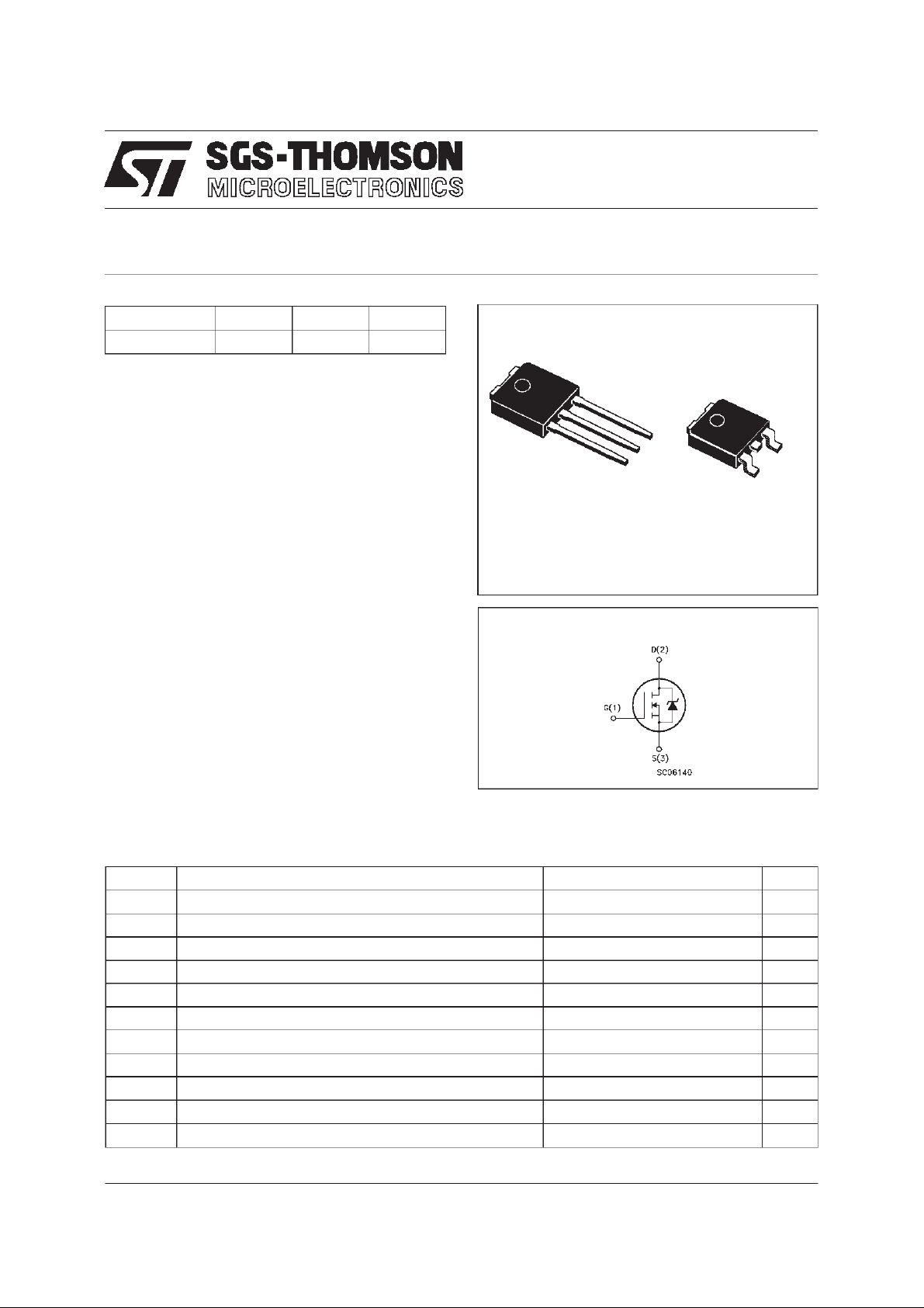
3
2
IPAK
TO-251
(Suffix”-1”)
1
(Suffix ”T4”)
1
DPAK
TO-252
INTERNAL SCHEMATIC DIAGRAM
3
ABSOLUTE MAXIMUM RATINGS
Symb o l Para meter Value Uni t
V
V
V
I
DM
P
dv/dt(
T
(•) Pulse width limited by safe operating area (1)ISD≤2.6A, di/dt ≤ 200 A/µs, VDD≤ V
March 1998
Drain-source Voltage (VGS=0) 600 V
DS
DGR Drain- gate Voltage (R
Gat e- source Vo lt age ± 30 V
GS
I
Drain Cur rent ( continuous) at Tc=25oC2.6A
D
I
Drain Cur rent ( continuous) at Tc=100oC1.6A
D
=20kΩ)
GS
600 V
(•) Dra in Cur rent ( pul sed) 10.4 A
Tot al Dissipation at Tc=25oC50W
tot
Derating Factor 0.4 W/
1) Peak Diode Rec overy volt age s l ope 4.5 V/ns
Sto rage Tempe rature -65 to 150
stg
T
Max. Operating Ju nc t io n Tem peratur e 150
j
,Tj≤T
(BR)DSS
JMAX
o
C
o
C
o
C
1/9
Page 2
STD2NB60
THERMAL DATA
R
thj-case
Rthj-a mb
R
thc-sin k
T
AVALANCHE CHARACTERISTICS
Symbol Para met e r Max Value Uni t
I
AR
E
Ther mal Resist ance Junctio n-c a se Max
Ther mal Resist ance Junctio n-ambient Max
Ther mal Resist ance Case-sink T yp
Maximum Lead Temperat u re F o r Soldering Purp ose
l
Avalanche Cur rent, Rep etit ive or Not-Re petitive
(pulse width limited by T
Single Pulse Avalanche Energy
AS
(starting T
=25oC, ID=IAR,VDD=50V)
j
max, δ <1%)
j
2.5
100
1.5
275
2.6 A
80 mJ
o
C/W
oC/W
o
C/W
o
C
ELECTRICAL CHARACTERISTICS (T
=25oC unlessotherwise specified)
case
OFF
Symbol Parameter Test Cond itions Min. Typ. M ax. Unit
V
(BR)DSS
Drain-sourc e
=250µAVGS=0
I
D
600 V
Breakdown V oltage
I
DSS
I
GSS
Zer o Gat e V o lt age
Drain Current (V
GS
Gat e-body Leaka ge
Current (V
DS
=0)
=0)
=MaxRating
V
DS
V
=MaxRating Tc=125oC
DS
= ± 30 V
V
GS
1
50
± 100 nA
ON (∗)
Symbol Parameter Test Cond itions Min. Typ. M ax. Unit
V
GS(th )
Gate Threshold
V
DS=VGSID
=250µA
345V
Voltage
R
DS(on)
Stati c D rain-source On
VGS=10V ID=1.6 A 3.3 3.6 Ω
Resistance
I
D(on)
On State Drain Curre nt VDS>I
D(on)xRDS(on)max
3.3 A
VGS=10V
DYNAMIC
Symbol Parameter Test Cond itions Min. Typ. M ax. Unit
g
(∗)Forward
fs
Tr ansconductanc e
C
C
C
Input Capac i t an c e
iss
Out put C apa c itance
oss
Reverse Transf er
rss
Capa cit an c e
VDS>I
D(on)xRDS(on)maxID
=1.6A 1.2 2 S
VDS=25V f=1MHz VGS= 0 400
57
7
520
77
9
µA
µA
pF
pF
pF
2/9
Page 3
STD2NB60
ELECTRICAL CHARACTERISTICS (continued)
SWITCHINGON
Symbol Parameter Test Cond itions Min. Typ. M ax. Unit
t
d(on)
Turn-on Time
r
Rise Time
t
VDD=300V ID=1.6A
=4.7 Ω VGS=10V
R
G
11
7
(see test circuit, figure 3)
Q
Q
Q
Total Gate Charge
g
Gat e-Sour ce Cha rge
gs
Gate-Drain Charge
gd
VDD=480V ID=3.3 A VGS=10V 15
6.2
5.6
SWITCHINGOFF
Symbol Parameter Test Cond itions Min. Typ. M ax. Unit
t
r(Voff)
t
t
Of f - voltage Rise Time
Fall Time
f
Cross-ov er Time
c
VDD=480V ID=3.3A
=4.7 Ω VGS=10V
R
G
(see test circuit, figure 5)
11
13
18
SOURCE DRAIN DIODE
Symbol Parameter Test Cond itions Min. Typ. M ax. Unit
I
SD
I
SDM
V
SD
t
Q
I
RRM
(∗) Pulsed: Pulse duration =300 µs, duty cycle1.5 %
(•) Pulse width limited by safe operating area
Source-drain Curre nt
(•)
Source-drain Curre nt
(pulsed)
(∗) For ward On Vo ltage ISD=3.3A VGS=0 1.6 V
Reverse Recov er y
rr
Time
Reverse Recov er y
rr
= 3.3 A di/dt = 100 A /µs
I
SD
=100V Tj=150oC
V
DD
(see test circuit, figure 5)
500
2.1
Charge
Reverse Recov er y
8.5
Current
17
11
22 nC
16
18
25
3.3
13.2
ns
ns
nC
nC
ns
ns
ns
A
A
ns
µC
A
Safe Operating Area ThermalImpedance
3/9
Page 4

STD2NB60
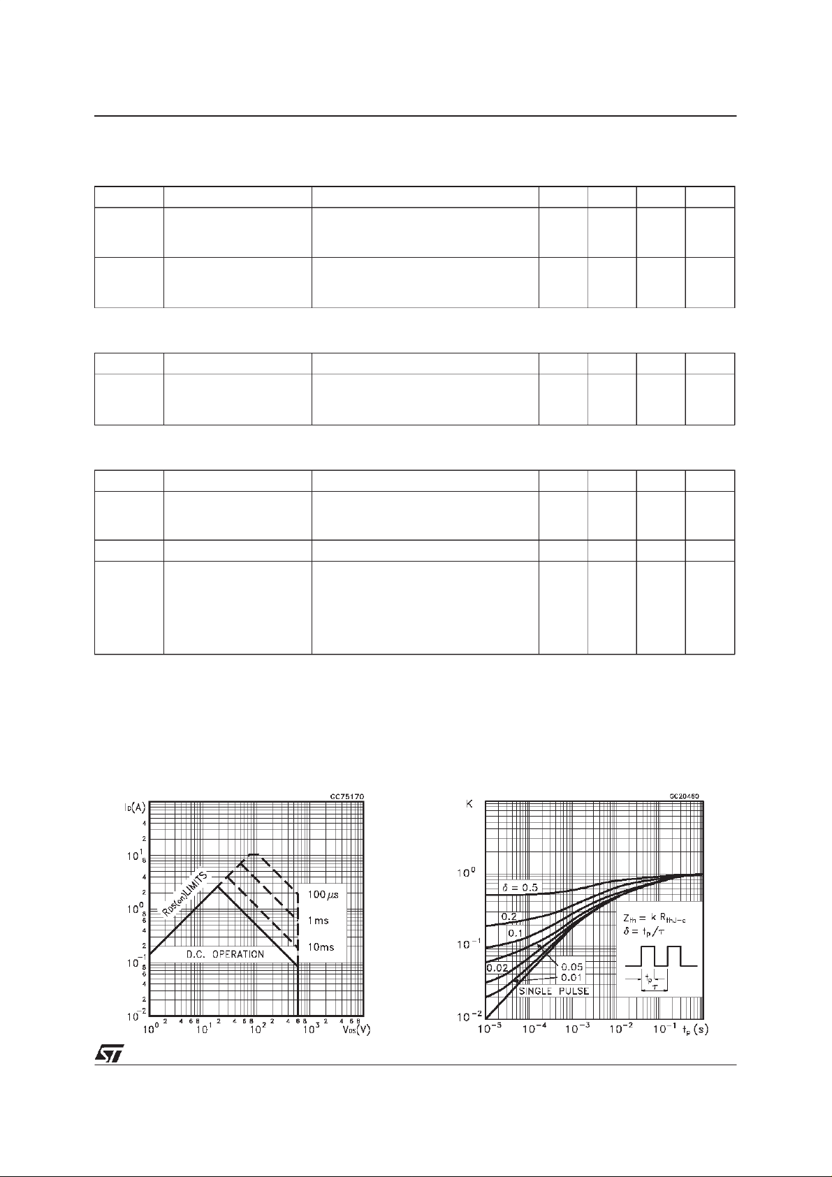
OutputCharacteristics
Transconductance
TransferCharacteristics
StaticDrain-sourceOn Resistance
GateCharge vs Gate-sourceVoltage
4/9
CapacitanceVariations
Page 5
STD2NB60
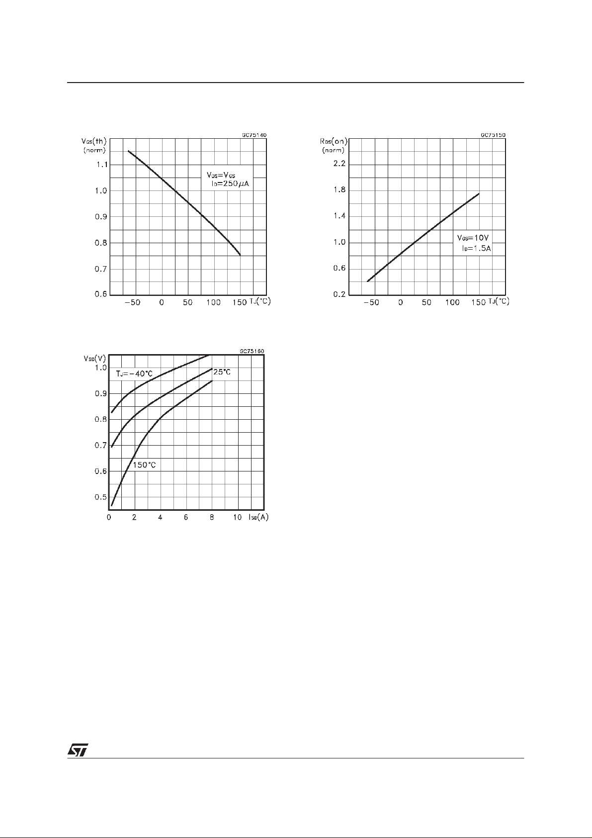
Normalized Gate Threshold Voltage vs
Temperature
Source-drainDiode Forward Characteristics
Normalized On Resistance vs Temperature
5/9
Page 6

STD2NB60
Fig. 1: Unclamped InductiveLoad TestCircuit
Fig. 3: SwitchingTimesTest CircuitsFor
ResistiveLoad
Fig. 2: Unclamped InductiveWaveform
Fig. 4: Gate Charge test Circuit
Fig. 5: Test Circuit For Inductive Load Switching
And Diode RecoveryTimes
6/9
Page 7
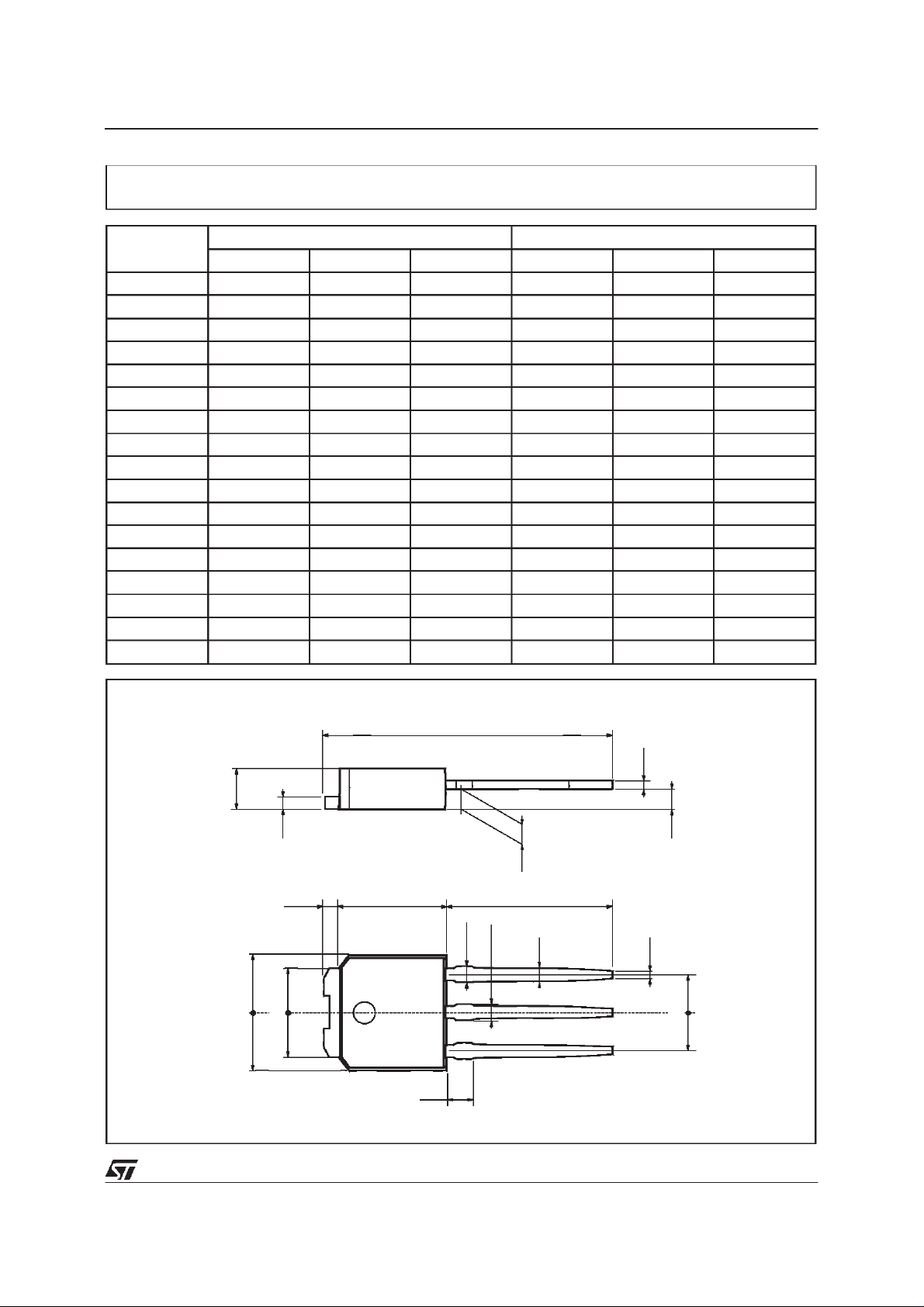
TO-251 (IPAK) MECHANICAL DATA
STD2NB60
DIM.
mm inch
MIN. TYP. MAX. MIN. TYP. MAX.
A 2.2 2.4 0.086 0.094
A1 0.9 1.1 0.035 0.043
A3 0.7 1.3 0.027 0.051
B 0.64 0.9 0.025 0.031
B2 5.2 5.4 0.204 0.212
B3 0.85 0.033
B5 0.3 0.012
B6 0.95 0.037
C 0.45 0.6 0.017 0.023
C2 0.48 0.6 0.019 0.023
D 6 6.2 0.236 0.244
E 6.4 6.6 0.252 0.260
G 4.4 4.6 0.173 0.181
H 15.9 16.3 0.626 0.641
L 9 9.4 0.354 0.370
L1 0.8 1.2 0.031 0.047
L2 0.8 1 0.031 0.039
A
E
==
C2
L2
B2
==
H
C
A3
A1
B6
L
B
B5
G
==
D
B3
2
13
L1
0068771-E
7/9
Page 8
STD2NB60
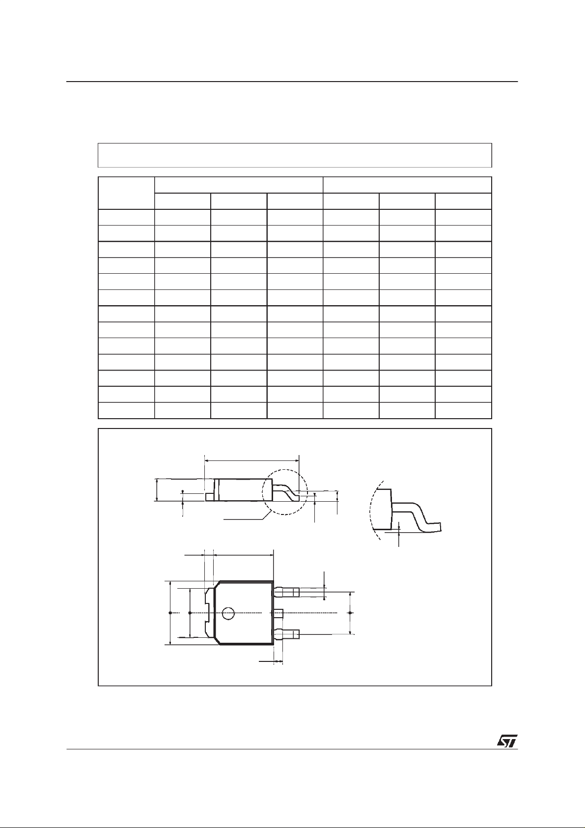
TO-252(DPAK) MECHANICAL DATA
DIM.
mm inch
MIN. TYP. MAX. MIN. TYP. MAX.
A 2.2 2.4 0.086 0.094
A1 0.9 1.1 0.035 0.043
A2 0.03 0.23 0.001 0.009
B 0.64 0.9 0.025 0.035
B2 5.2 5.4 0.204 0.212
C 0.45 0.6 0.017 0.023
C2 0.48 0.6 0.019 0.023
D 6 6.2 0.236 0.244
E 6.4 6.6 0.252 0.260
G 4.4 4.6 0.173 0.181
H 9.35 10.1 0.368 0.397
L2 0.8 0.031
L4 0.6 1 0.023 0.039
H
8/9
A
E
C2
L2
B2
==
==
DETAIL”A”
D
2
13
L4
A1
C
A2
DETAIL”A”
B
G
==
0068772-B
Page 9

STD2NB60
Information furnished is believed to be accurate and reliable. However, SGS-THOMSON Microelectronics assumes no responsability for the
consequences of use of such information nor for any infringement of patents orother rights of third parties which may results from itsuse. No
license is granted by implication or otherwise under any patent orpatent rights of SGS-THOMSON Microelectronics. Specifications mentioned
in thispublication are subject to change without notice. This publication supersedes and replaces all information previously supplied.
SGS-THOMSON Microelectronics productsarenot authorizedfor use as critical componentsin life support devices orsystems withoutexpress
written approval ofSGS-THOMSON Microelectonics.
1998 SGS-THOMSON Microelectronics - Printed in Italy - All Rights Reserved
Australia - Brazil - Canada - China - France - Germany - Italy - Japan - Korea - Malaysia - Malta - Morocco - The Netherlands -
Singapore - Spain - Sweden - Switzerland - Taiwan - Thailand - United Kingdom -U.S.A
SGS-THOMSON Microelectronics GROUP OF COMPANIES
...
9/9
 Loading...