

Page 1
STD2NA50
N - CHANNEL ENHANCEMENT MODE
POWER MOS TRANSISTOR
PRELIMINARY DATA
■ TYPICAL R
DS(on)
= 3.25 Ω
■ ± 30V GATE TO SOURCE VOLTA GE RATING
■ 100% AVALANCHE TESTED
■ REPETITIVE AVA LANCHE DATA AT 100
o
C
■ LOW INTRINSIC CAPACITANCES
■ GATE CH ARGE MINIMIZED
■ REDUCED THRESHOLD VO LTA GE SPREA D
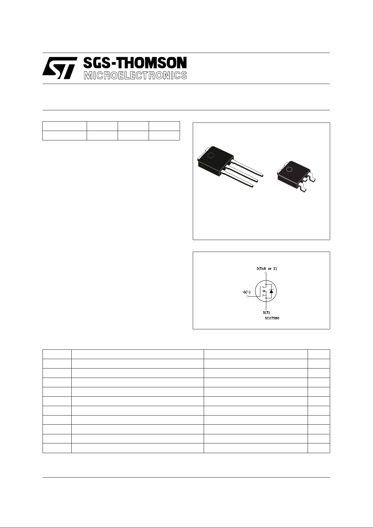
■ THROUGH-HO LE IPAK (TO -251) POWE R
PACKAGE IN TU BE (SUFFIX "-1")
■ SURFACE-MOUNTING DPAK (TO-252)
POWER PACKAGE IN TAPE & REEL
(SUFFIX "T4")
APPLICATIONS
■ MEDIUM CURRENT, HIGH SPEED
SWITCHING
■ SWITCH MODE P OW ER SUP P LIE S (S MP S)
■ CONSUMER AND INDUSTRIAL LIGHTING
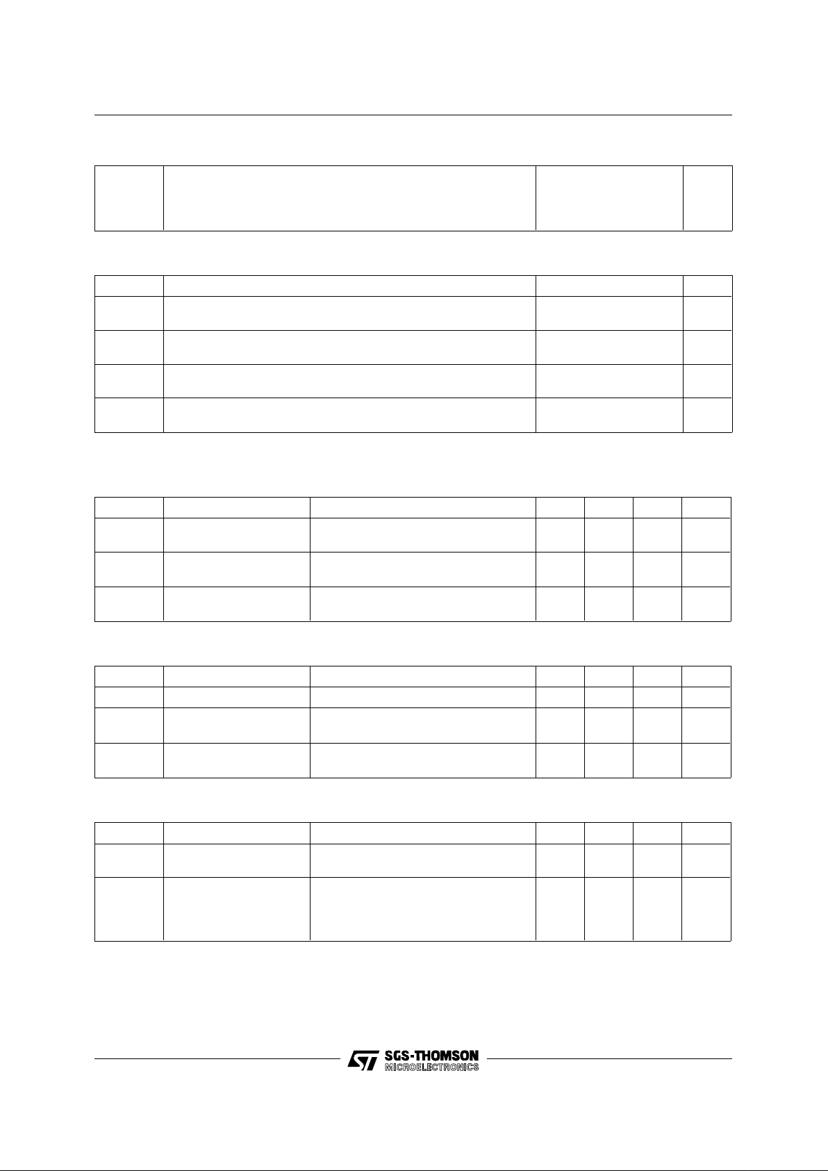
INTERNAL SCHEMATIC DIAGRAM
ABSOL UT E MAXIMU M RATINGS
Symbol Parameter Value Unit
V
DS
Drain-source Voltage (VGS = 0) 500 V
V
DGR
Drain- gate Voltage (RGS = 20 kΩ) 500 V
V
GS
Gate-source Voltage ± 30 V
I
D
Drain Current (continuous) at Tc = 25 oC 2.2 A
I
D
Drain Current (continuous) at Tc = 100 oC 1.4 A
I
DM
(•) Drain Current (pulsed) 8.8 A
P
tot
Total Dissipation at Tc = 25 oC45W
Derating Factor 0.36 W/
o
C
T
stg
Storage Temperature -65 to 150
o
C
T
j
Max. Operating Junction Temperature 150
o
C
(•) Pulse width limited by safe operating area
TYPE V
DSS
R
DS(on)
I
D
STD2NA50 500 V < 4 Ω 2.2 A
March 1996
3
2
1
IPAK
TO-251
(Suffix "- 1")
1
3
DPAK
TO-252
(Suffix "T4")
1/6
Page 2
THERMAL DATA
R
thj-case
R
thj-amb
R
thc-si n k
T
l
Thermal Resistance Junction-case Max
Thermal Resistance Junction-ambient Max
Thermal Resistance Case-sink Typ
Maximum Lead Temperature For Soldering Purpose
2.78
100
1
275
o
C/W
o
C/W
o
C/W
o
C
AVALANCHE CHARACTERI S TICS
Symbol Parameter Max Value Unit
I
AR
Avalanche Current, Repetitive or Not-Repetitive
(pulse width limited by T
j
max, δ < 1%)
2.2 A
E
AS
Single Pulse Avalanche Energy
(starting T
j
= 25 oC, ID = IAR, V
DD
= 50 V)
25 mJ
E
AR
Repetitive Avalanche Energy
(pulse width limited by T
j
max, δ < 1%)
1mJ
I
AR
Avalanche Current, Repetitive or Not-Repetitive
(T
c
= 100 oC, pulse width limited by Tj max, δ < 1%)
1.4 A
ELECTRICAL CHARACTERISTICS (T
case
= 25 oC unless otherwise specified)
OFF
Symbol Parameter Test Conditions Min. Typ. Max. Unit
V
(BR)DSS
Drain-source
Breakdown Voltage
ID = 250 µA V
GS
= 0 500 V
I
DSS
Zero Gate Voltage
Drain Current (V
GS
= 0)
V
DS
= Max Rating
V
DS
= Max Rating x 0.8 Tc = 125 oC
250
1000µAµA
I
GSS
Gate-Source Leakage
Current (V
DS
= 0)
V
GS
= ± 30 V 100 mA
ON (∗)
Symbol Parameter Test Conditions Min. Typ. Max. Unit
V
GS(th)
Gate Threshold Voltage V
DS
= V
GS ID
= 250 µA 2.25 3 3.75 V
R
DS(on)
Static Drain-source On
Resistance
VGS = 10 V ID = 1.1 A
V
GS
= 10 V ID = 1.1 A Tc = 100oC
3.25 4
8
Ω
Ω
I
D(on)
On State Drain Current VDS > I
D(on)
x R
DS(on)max
V
GS
= 10 V
2.2 A
DYNAMIC
Symbol Parameter Test Conditions Min. Typ. Max. Unit
g
fs
(∗) Forward
Transconductance
VDS > I
D(on)
x R
DS(on)max
ID = 1.1 A 0.7 1.9 S
C
iss
C
oss
C
rss
Input Capacitance
Output Capacitance
Reverse Transfer
Capacitance
V
DS
= 25 V f = 1 MHz V
GS
= 0 300
55
15
400
70
20
pF
pF
pF
STD2NA50
2/6
Page 3

ELECTRICAL CHARACTERISTICS (continued)
SWITCHING O N
Symbol Parameter Test Conditions Min. Typ. Max. Unit
t
d(on)
t
r
Turn-on Time
Rise Time
V
DD
= 250 V ID = 1.1 A
R
G
= 4.7 Ω VGS = 10 V
7
8
10
11
ns
ns
(di/dt)
on
Turn-on Current Slope V
DD
= 400 V ID = 2.2 A
R
G
= 47 Ω VGS = 10 V
350 A/µs
Q
g
Q
gs
Q
gd
Total Gate Charge
Gate-Source Charge
Gate-Drain Charge
V
DD
= 400 V ID =2.2 A V
GS
= 10 V 18
5.5
7
25 nC
nC
nC
SWITCHING O F F
Symbol Parameter Test Conditions Min. Typ. Max. Unit
t
r(Voff)
t
f
t
c
Off-voltage Rise Time
Fall Time
Cross-over Time
V
DD
= 400 V ID = 2.2 A
R
G
= 4.7 Ω VGS = 10 V
7
7
14
10
10
20
ns
ns
ns
SOURCE DRAIN DIO DE
Symbol Parameter Test Conditions Min. Typ. Max. Unit
I
SD
I
SDM
(•)
Source-drain Current
Source-drain Current
(pulsed)
2.2
8.8
A
A
V
SD
(∗) Forward On Voltage ISD = 2.2 A VGS = 0 1.6 V
t
rr
Q
rr
I
RRM
Reverse Recovery
Time
Reverse Recovery
Charge
Reverse Recovery
Current
I
SD
= 2.2 A di/dt = 100 A/µs
V
DD
= 100 V Tj = 150 oC
380
4.4
23
ns
µC
A
(∗) Pulsed: Pulse duration = 300 µs, duty cycle 1.5 %
(•) Pulse width limited by safe operating area
STD2NA50
3/6
Page 4

DIM.
mm inch
MIN. TYP. MAX. MIN. TYP. MAX.
A 2.2 2.4 0.086 0.094
A1 0.9 1.1 0.035 0.043
A3 0.7 1.3 0.027 0.051
B 0.64 0.9 0.025 0.031
B2 5.2 5.4 0.204 0.212
B3 0.85 0.033
B5 0.3 0.012
B6 0.95 0.037
C 0.45 0.6 0.017 0.023
C2 0.48 0.6 0.019 0.023
D 6 6.2 0.236 0.244
E 6.4 6.6 0.252 0.260
G 4.4 4.6 0.173 0.181
H 15.9 16.3 0.626 0.641
L 9 9.4 0.354 0.370
L1 0.8 1.2 0.031 0.047
L2 0.8 1 0.031 0.039
A
C2
C
A3
H
A1
D
L
L2
L1
1 3
= =
B3
B
B6
B2
E
G
= =
= =
B5
2
TO-251 (IPAK) MECHANI CAL DAT A
0068771-E
STD2NA50
4/6
Page 5

DIM.
mm inch
MIN. TYP. MAX. MIN. TYP. MAX.
A 2.2 2.4 0.086 0.094
A1 0.9 1.1 0.035 0.043
A2 0.03 0.23 0.001 0.009
B 0.64 0.9 0.025 0.035
B2 5.2 5.4 0.204 0.212
C 0.45 0.6 0.017 0.023
C2 0.48 0.6 0.019 0.023
D 6 6.2 0.236 0.244
E 6.4 6.6 0.252 0.260
G 4.4 4.6 0.173 0.181
H 9.35 10.1 0.368 0.397
L2 0.8 0.031
L4 0.6 1 0.023 0.039
==
D
L2
L4
1 3
==
B
E
==
B2
G
2
A
C2
C
H
A1
DETAIL "A"
A2
DETAIL "A"
TO-252 (DPAK) MECHANICAL DATA
0068772-B
STD2NA50
5/6
Page 6

Information furnished is believed to be accurate and reliable. However, SGS-THOMSON Microelectronics assumes no responsability for the
consequences of use of such information nor for any infringement of pat e nts or ot her rights o f third partie s which may results from its use. No
license is granted by implication or otherwise under any patent or patent rights of SG S-THOMSON Microelectroni cs. Specifications ment ioned
in this publication are subject to cha nge wi t hout n o tice. This p u bli ca t ion sup e rsed e s and r epla ces al l inf ormat i on pr ev io us ly supplied.
SGS-THOMSON Microelectronics products are not auth orized for use as critical components in life support devices or systems without express
written approval of SGS-THOM SO N M icroelecto nics.
© 1995 SGS-THOMSON Microelectronics - All Rights Reserved
SGS-THOMSON Microelectronics GROUP OF COMPANIES
Australia - Brazil - France - Germany - Hong Ko ng - Ita ly - Japa n - Korea - Mal ay sia - Mal ta - Mor oc co - The Net her l ands -
Singapore - Spain - Sweden - Switzerland - Taiwan - Thailand - United Kingdom - U.S.A
. . .
STD2NA50
6/6
 Loading...