

Page 1
STD20NF10
N-CH A NNEL 100V - 0.038 Ω - 25A IPAK/DPAK
LOW GATE CHARGE STripFET™ II POWER MOSFET
TYPE
V
DSS
STD20NF10 100 V <0.045
■ TYPICAL R
■ EXCEPTIONA L dv/d t CAPABILITY
■ APPLICATION ORIENTED
(on) = 0.038 Ω
DS
R
DS(on)
I
D
25 A(*)
Ω
CHARACTERIZATION
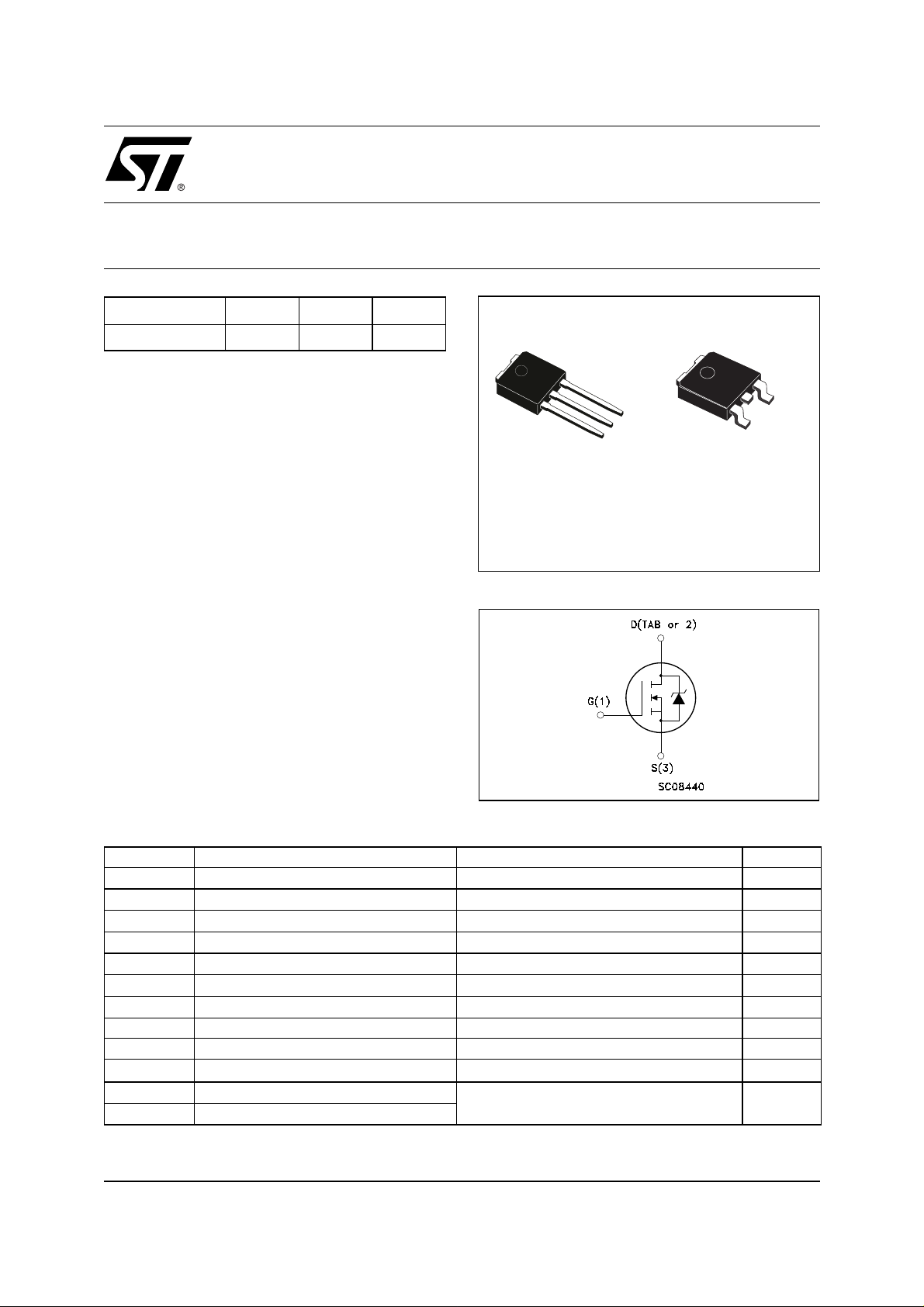
■ THROUGH-HOLE IPAK (TO-251) POWER
PACKAGE IN TUBE (SUFFIX “- 1 ")
■ SURFACE-MOUNTING DPAK (TO-252)
POWER PACKAGE IN TAPE & REEL
(SUFFIX “T4")
DESCRIPTION
This MOSFET series realized with STMicroelectronics
unique STripFET process has specifically been designed
to minimize input capacitance and gate charge. It is
therefore suitable as primary switch in advanced highefficiency, high-frequency isolate d DC-DC c onverters for
Telecom and Computer a pplications. It is also intended
for any applications with low gate drive requirements.
APPLICATIONS
■ HIGH-EFFICIENCY DC-DC CONVERTERS
■ UPS AND MOTOR CONTROL
3
2
1
IPAK
TO-251
(Suffix “-1”)
DPAK
TO-252
(Suffix “T4”)
INTERNAL SCHEMATIC DIAGRAM
3
1
ABSOLUTE MAXIMUM RATINGS
Symbol Parameter Value Unit
V
DS
V
DGR
V
GS
(*) Drain Current (continuous) at T
I
D
I
D
(
I
DM
P
tot
dv/dt
E
AS
T
stg
T
j
(
Pulse widt h l i m i ted by safe operating area.
•)
(*) Curren t Lim i ted by Package
.
Drain-source Voltage (VGS = 0)
Drain-gate Voltage (RGS = 20 kΩ)
100 V
100 V
Gate- source Voltage ± 20 V
= 25°C
C
Drain Current (continuous) at TC = 100°C
•)
Drain Current (pulsed) 100 A
Total Dissipation at TC = 25°C
25 A
21 A
85 W
Derating Factor 0.57 W/°C
(1)
Peak Diode Recovery voltage slope 20 V/ns
(2)
Single Pulse Avalanche Energy 300 mJ
Storage Temperature
Operating Junction Temperature
≤25A, di/dt ≤300A/ µ s , VDD ≤ V
(1) I
SD
(2) Starting Tj = 25 oC, ID = 10 A, VDD = 27V
-55 to 175 °C
(BR)DSS
, Tj ≤ T
JMAX
1/9October 2002
Page 2
STD20NF10
THERMA L D ATA
Rthj-case
Rthj-amb
T
Thermal Resistance Junction-case
Thermal Resistance Junction-ambient
Maximum Lead Temperature For Soldering Purpose
l
Max
Max
Typ
1.76
100
300
°C/W
°C/W
°C
ELECTRICAL CHARACTERISTICS (T
= 25 °C UNLESS OTHERWISE SPECIFIED)
CASE
OFF
Symbol Parameter Test Conditions Min. Typ. Max. Unit
I
= 250 µA, VGS = 0
D
V
= Max Rating
DS
V
= Max Rating TC = 125°C
DS
V
= ± 20V
GS
100 V
1
10
±1 µA
ON
V
(BR)DSS
I
DSS
I
GSS
(1)
Drain-source
Breakdown Voltage
Zero Gate Voltage
Drain Current (V
GS
Gate-body Leakage
Current (V
DS
= 0)
= 0)
Symbol Parameter Test Conditions Min. Typ. Max. Unit
V
V
GS(th)
R
DS(on)
Gate Threshold Voltage
Static Drain-source On
Resistance
= VGS I
DS
V
= 10 V ID = 15 A
GS
= 250 µA
D
234V
0.038 0.045
DYNAMIC
Symbol Parameter Test Conditions Min. Typ. Max. Unit
(*)
g
fs
C
iss
C
oss
C
rss
Forward Transconductance
Input Capacitance
Output Capacitance
Reverse Transfer
Capacitance
V
= 15 V ID= 15 A
DS
= 25V, f = 1 MHz, VGS = 0
V
DS
10 S
1200
180
80
µA
µA
Ω
pF
pF
pF
2/9
Page 3
STD20NF10
ELECTRICAL CHARACTERISTICS (continued)
SWITCHING ON
Symbol Parameter Test Conditions Min. Typ. Max. Unit
= 50 V ID = 15 A
t
d(on)
Turn-on Delay Time
t
r
Rise Time
V
DD
R
= 4.7 Ω VGS = 10 V
G
(Resistive Load, Figure 3)
Q
g
Q
gs
Q
gd
Total Gate Charge
Gate-Source Charge
Gate-Drain Charge
= 80 V ID= 30 A VGS=10 V
V
DD
SWITCHING OFF
Symbol Parameter Test Conditions Min. Typ. Max. Unit
= 50 V ID = 15 A
t
d(off)
Turn-off Delay Time
t
f
Fall Time
V
DD
R
= 4.7Ω, V
G
GS
= 10 V
(Resistive Load, Figure 3)
SOURCE DRAIN DIODE
Symbol Parameter Test Conditions Min. Typ. Max. Unit
I
SD
I
SDM
V
SD
t
rr
Q
rr
I
RRM
(*)
Pulsed: P ul se duration = 300 µs, duty cycle 1. 5 %.
(
Pulse widt h l i m i ted by safe ope rating area.
•)
Source-drain Current
(•)
Source-drain Current (pulsed)
(*)
Forward On Voltage
Reverse Recovery Time
Reverse Recovery Charge
Reverse Recovery Current
I
= 20 A VGS = 0
SD
= 30 A di/dt = 100A/µs
I
SD
V
= 55 V Tj = 150°C
DD
(see test circuit, Figure 5)
15
40
40
8
15
45
10
110
390
7.5
55 nC
30
120
1.3 V
ns
ns
nC
nC
ns
ns
A
A
ns
µ
A
C
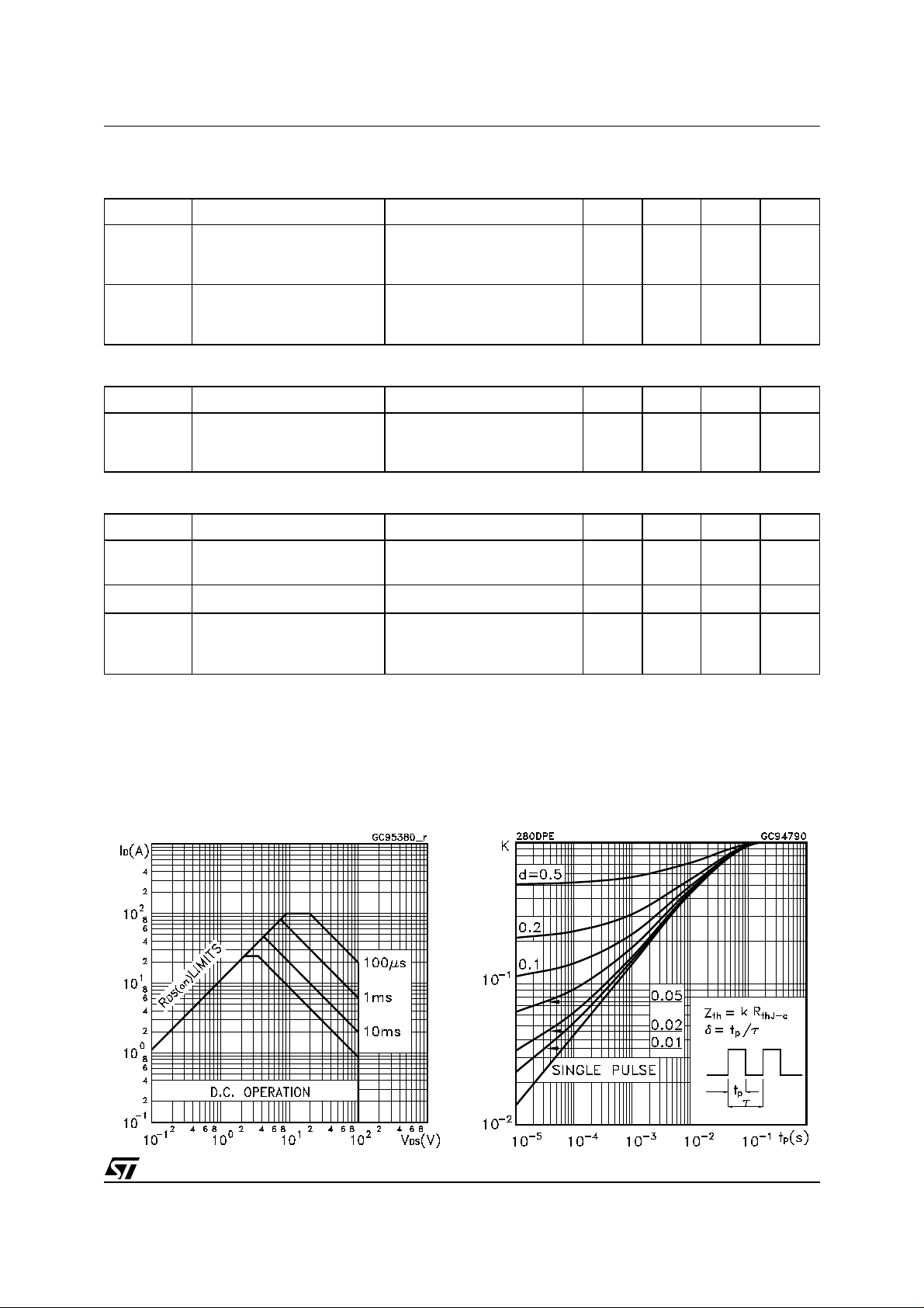
Saf e Oper ating A rea
Thermal Impedance
3/9
Page 4

STD20NF10
Output Characteristics Transfer Characteristics
Transconductance Static Drain-source On Resistance
Gate Charge vs Gate-source Voltage Capacitance Variations
4/9
Page 5

STD20NF10
Normalized Gate Threshold Voltage vs Temperature Normalized on Resistance vs Temperature
Source-drain Diode Forward Characteristics Normalized Breakdown Voltage Temperature
. .
5/9
Page 6

STD20NF10
Fig. 1: Unclamped Inductive Load Test CircuitFig. 1: Unclamped Inductive Load Test Circuit Fig. 2: Unclam ped Induc tive Waveform
Fig. 3: Switching Times Test Circuits For Resistive
Load
Fig. 5: Test Circuit For Inductive Load Switching
And Diode Recovery Times
Fig. 4: Gate Charge test Circuit
6/9
Page 7

STD20NF10
TO-251 (IPAK) MECHANI CAL DAT A
DIM.
mm inch
MIN. TYP. MAX. MIN. TYP. MAX.
A 2.2 2.4 0.086 0.094
A1 0.9 1.1 0.035 0.043
A3 0.7 1.3 0.027 0.051
B 0.64 0.9 0.025 0.031
B2 5.2 5.4 0.204 0.212
B3 0.85 0.033
B5 0.3 0.012
B6 0.95 0.037
C 0.45 0.6 0.017 0.023
C2 0.48 0.6 0.019 0.023
D 6 6.2 0.236 0.244
E 6.4 6.6 0.252 0.260
G 4.4 4.6 0.173 0.181
H 15.9 16.3 0.626 0.641
L 9 9.4 0.354 0.370
L1 0.8 1.2 0.031 0.047
L2 0.8 1 0.031 0.039
A
C2
L2
E
B2
= =
= =
H
C
A3
A1
B6
L
B
B5
G
= =
D
B3
2
1 3
L1
0068771-E
7/9
Page 8

STD20NF10
TO-252 (DPAK) MECHANICAL DATA
DIM.
mm inch
MIN. TYP. MAX. MIN. TYP. MAX.
A 2.2 2.4 0.086 0.094
A1 0.9 1.1 0.035 0.043
A2 0.03 0.23 0.001 0.009
B 0.64 0.9 0.025 0.035
B2 5.2 5.4 0.204 0.212
C 0.45 0.6 0.017 0.023
C2 0.48 0.6 0.019 0.023
D 6 6.2 0.236 0.244
E 6.4 6.6 0.252 0.260
G 4.4 4.6 0.173 0.181
H 9.35 10.1 0.368 0.397
L2 0.8 0.031
L4 0.6 1 0.023 0.039
A
C2
L2
E
B2
==
H
DETAIL "A"
D
==
C
B
2
1 3
L4
A1
G
==
A2
DETAIL "A"
0068772-B
8/9
Page 9

STD20NF10
Information furnished is believed to be accurate and reliable. However, STMicroelectronics assumes no responsibility for the consequences
of use of such information nor for any infringement of patents or other rights of third parties which may result from its use. No license is granted
by implic ation or otherwise unde r any patent or patent right s of STMic roelectronics. Specifications ment i oned in this p ublication are subject
to change without notice. This publication supersedes and replaces all information previously supplied. STMicroelectronics product s are not
authorized for use as crit i cal component s in l i fe support devi ces or systems wi t hout express written approva l of STMicroelectronics.
The ST logo is registered trademark of STMicroelectronics
2002 STMi croelectroni cs - All Rights Reserved
All other na m es are the property of their respective owner s.
Australi a - Brazil - Cana da - China - Finland - France - Ge rmany - Hong Ko ng - India - Israel - It al y - Japan - Malaysia - Malt a - Morocco -
Singap ore - Spain - Sweden - Switzerl and - United Ki ngdom - United S tates.
STMicroelectronics GROUP OF COMPANIES
http:// www.st.com
9/9
 Loading...