

Page 1
STD20NE06
N - CHANNEL ENHANCEMENT MODE
” SINGLE FEATURE SIZE ” POWER MOSFET
TYPE V
DSS
R
DS(on)
I
D
STD20NE06 60 V < 0.040 Ω 20 A
■ TYPICALR
■ EXCEPTIONAL dv/dt CAPABILITY
■ 100% AVALANCHETESTED
■ APPLICATIONORIENTED
DS(on)
=0.032 Ω
CHARACTERIZATION
■ FOR THROUGH-HOLE VERSIONCONTACT
SALESOFFICE
DESCRIPTION
This Power MOSFET is the latest development of
SGS-THOMSON unique ”Single Feature Size”
strip-based process. The resulting transistor
shows extremelyhigh packing density for low onresistance, rugged avalanche characteristics and
less critical alignment steps therefore a remarkable manufacturingreproducibility.
APPLICATIONS
■ SOLENOIDANDRELAY DRIVERS
■ MOTORCONTROL, AUDIOAMPLIFIERS
■ DC-DCCONVERTERS
■ AUTOMOTIVE ENVIRONMENT
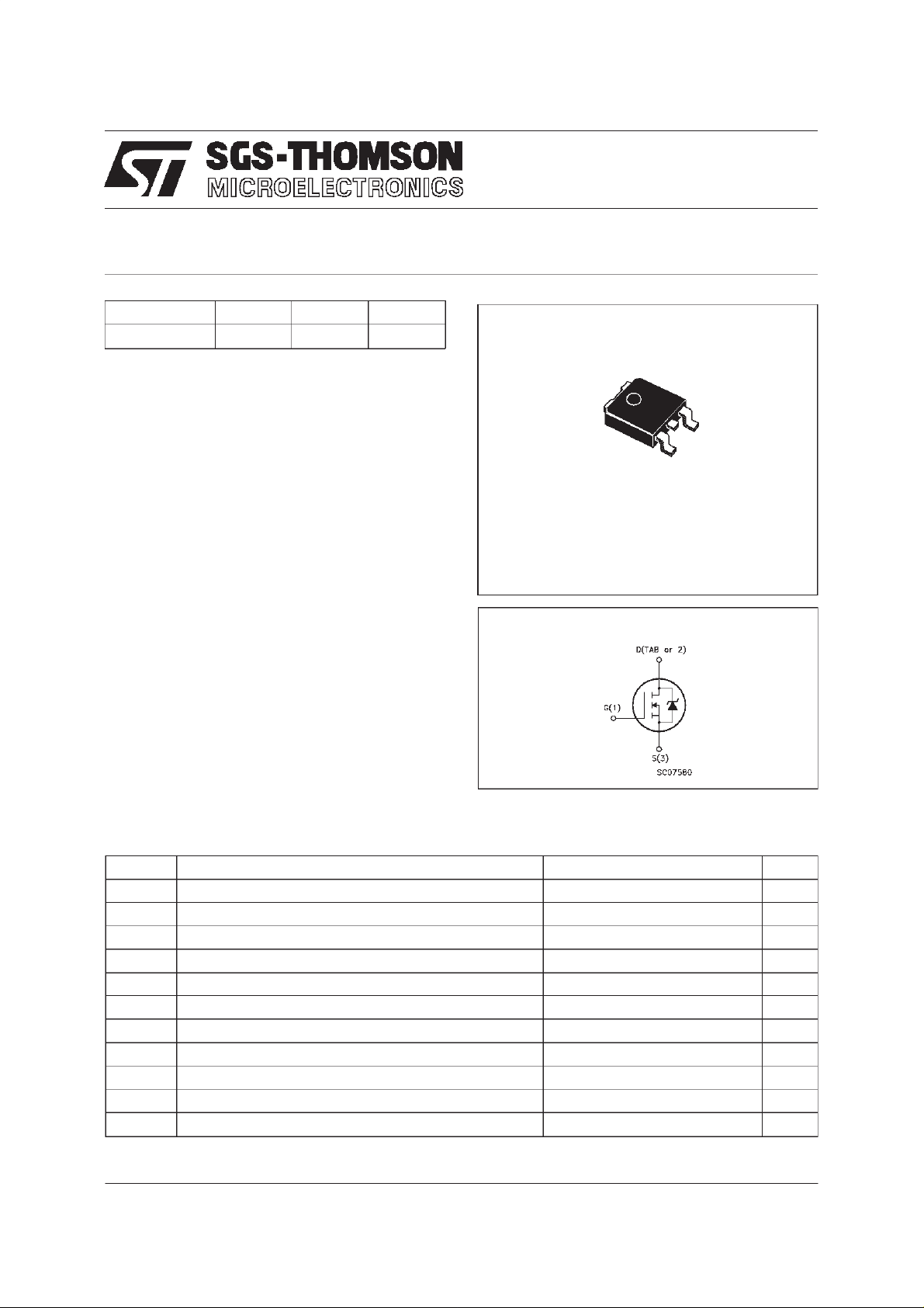
3
1
DPAK
TO-252
(Suffix ”T4”)
INTERNAL SCHEMATIC DIAGRAM
ABSOLUTE MAXIMUM RATINGS
Symb o l Para meter Value Uni t
V
V
V
I
DM
P
dv/ dt Peak Diode Recov ery vo lt age sl ope 7 V/ns
T
(•) Pulsewidth limitedby safe operating area (1)ISD≤ 36 A,di/dt ≤ 300 A/µs, VDD≤ V
January 1998
Drain-source Voltage (VGS=0) 60 V
DS
Drain- gate Voltage ( RGS=20kΩ)
DGR
Gat e- source Volt age ± 20 V
GS
I
Drain Current (c on t in uous) at Tc=25oC 20** A
D
I
Drain Current (c on t in uous) at Tc=100oC17A
D
60 V
(•) Drain Current (pulsed) 80 A
Tot al Dissip at i on at Tc=25oC50W
tot
Derating Factor 0.33 W/
Sto rage T emperat ure -65 to 175
stg
T
Max. Oper at in g Junc t io n Temperatur e 175
j
(**) Value limited only by the package
(BR)DSS,Tj≤TJMAX
o
C
o
C
o
C
1/8
Page 2
STD20NE06
THERMAL DATA
R
thj-case
Rthj-amb
R
thc-sin k
T
AVALANCHE CHARACTERISTICS
Symbol Para met e r Max Va lu e Uni t
I
AR
E
Ther mal Resist ance Junction- case Max
Ther mal Resist ance Junction- ambient Max
Ther mal Resist ance Case-sink Ty p
Maximum Lead Tempera t ure For Sold ering Purpose
l
Avalanche Current, Repetit i v e or Not-Repetitive
(pulse w idth limited by T
Single Pulse Avalanche Energy
AS
(starting T
=25oC, ID=IAR,VDD=25V)
j
max, δ <1%)
j
3.0
100
1.5
275
20 A
80 mJ
o
C/W
oC/W
o
C/W
o
C
ELECTRICAL CHARACTERISTICS (T
=25oC unlessotherwise specified)
case
OFF
Symbol Parameter Test Cond itions Min. Typ. Max. Un it
V
(BR)DSS
Drain-source
=250µAVGS=0
I
D
60 V
Breakdown Voltage
I
DSS
I
GSS
Zer o Gate Vo lt age
Drain Cur re nt (V
GS
Gat e-body Leakage
Current (V
DS
=0)
=0)
=MaxRating
V
DS
V
=MaxRating Tc=125
DS
o
C
= ± 20 V
V
GS
1
10
± 100 nA
ON (∗)
Symbol Parameter Test Cond itions Min. Typ. Max. Un it
V
GS(th )
Gate Threshold
V
DS=VGSID
=250µA
234V
Voltage
R
DS(on)
Stati c Drain-so urce On
VGS=10V ID=10A 0.032 0.04 Ω
Resistance
I
D(on)
On State Drain Cu rr e nt VDS>I
D(on)xRDS(on)max
20 A
VGS=10V
DYNAMIC
Symbol Parameter Test Cond itions Min. Typ. Max. Un it
g
(∗)Forward
fs
Tr ansconductance
C
C
C
Input Capaci t ance
iss
Out put Capa citance
oss
Reverse Transfer
rss
Capa cit an c e
VDS>I
D(on)xRDS(on)maxID
=10 A 7 13 S
VDS=25V f=1MHz VGS= 0 2115
260
65
2800
350
90
µA
µA
pF
pF
pF
2/8
Page 3
STD20NE06
ELECTRICAL CHARACTERISTICS (continued)
SWITCHINGON
Symbol Parameter Test Cond itions Min. Typ. Max. Un it
t
d(on)
t
r
(di/dt)
Q
Q
gs
Q
gd
Turn-on Time
Rise Tim e
Turn-on Current Slope VDD=48V ID=36A
on
Total Gate Charge
g
VDD=30V ID=18A
=4.7 Ω VGS=10V
R
G
=47 Ω VGS=10 V
R
G
VDD=48V ID=36A VGS=10V 50
Gat e-Sourc e Charge
Gate-Drain Charge
28
85
250 A/µs
13
18
SWITCHINGOFF
Symbol Parameter Test Cond itions Min. Typ. Max. Un it
t
r(Voff)
t
t
Of f - voltage Rise T im e
Fall Time
f
Cross-over Time
c
VDD=48V ID=36A
=4.7 Ω VGS=10V
R
G
12
25
40
SOURCE DRAIN DIODE
Symbol Parameter Test Cond itions Min. Typ. Max. Un it
I
SD
I
SDM
V
SD
t
Q
I
RRM
(∗) Pulsed: Pulseduration =300 µs, duty cycle 1.5 %
(•) Pulse widthlimited by safe operating area
Source-drain Current
(•)
Source-drain Current
(pulsed)
(∗) For ward O n Vo lt age ISD=20A VGS=0 1.5 V
Reverse Recover y
rr
Time
Reverse Recover y
rr
= 36 A di/dt = 10 0 A/µs
I
SD
=30V Tj=150oC
V
DD
75
245
Charge
Reverse Recover y
6.5
Current
40
115
70 nC
16
35
55
20
80
ns
ns
nC
nC
ns
ns
ns
A
A
ns
nC
A
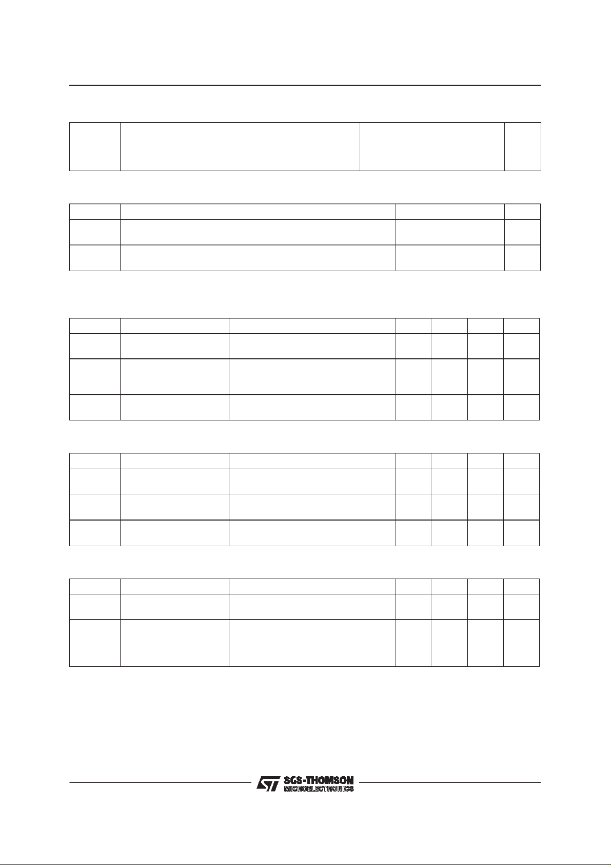
Safe Operating Area ThermalImpedance
3/8
Page 4

STD20NE06
OutputCharacteristics
Transconductance
TransferCharacteristics
StaticDrain-sourceOn Resistance
GateCharge vs Gate-sourceVoltage
4/8
CapacitanceVariations
Page 5
STD20NE06
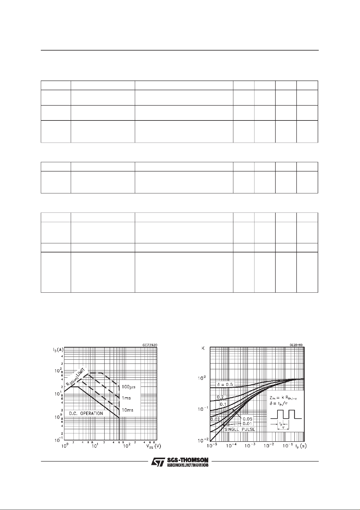
Normalized GateThresholdVoltage vs
Temperature
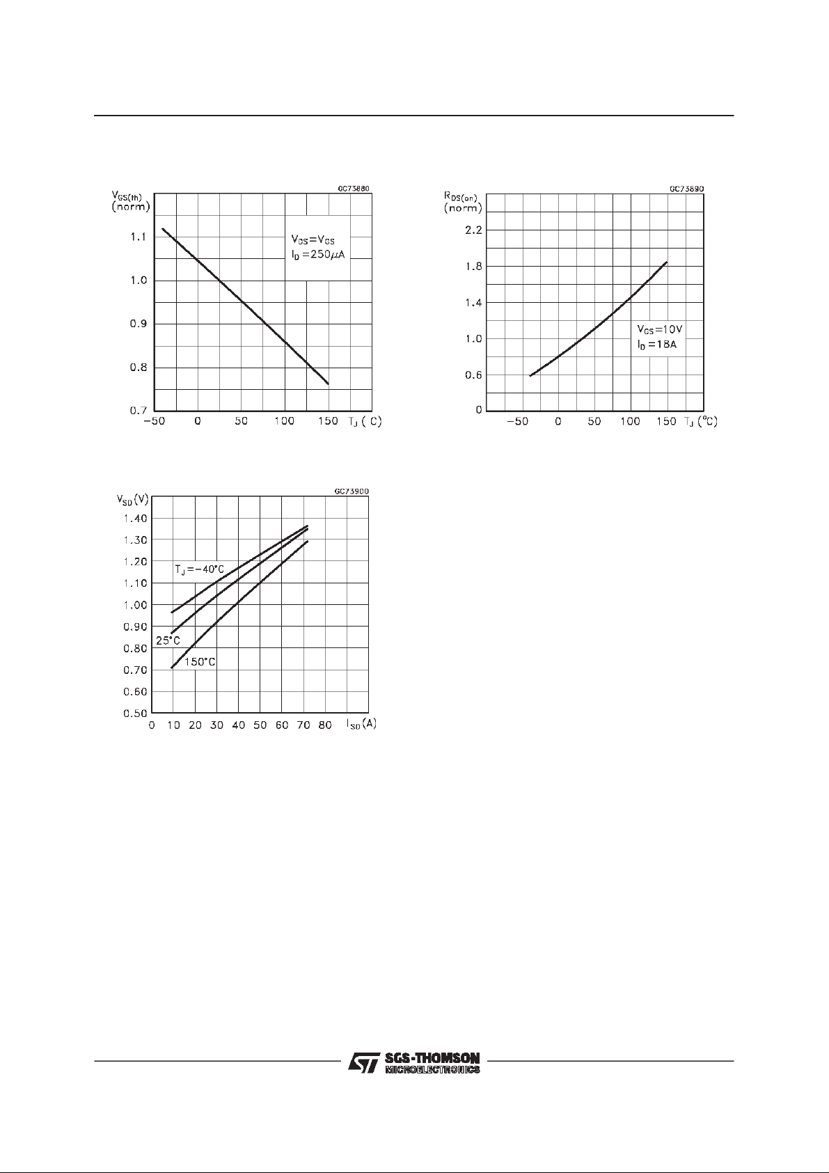
Source-drainDiode Forward Characteristics
Normalized On Resistancevs Temperature
5/8
Page 6

STD20NE06
Fig. 1: UnclampedInductiveLoad Test Circuit
Fig. 3: Switching Times Test CircuitsFor
ResistiveLoad
Fig. 2: UnclampedInductive Waveform
Fig. 4: Gate Charge test Circuit
Fig. 5: Test Circuit For Inductive Load Switching
And Diode RecoveryTimes
6/8
Page 7

TO-252 (DPAK) MECHANICAL DATA
STD20NE06
DIM.
mm inch
MIN. TYP. MAX. MIN. TYP. MAX.
A 2.2 2.4 0.086 0.094
A1 0.9 1.1 0.035 0.043
A2 0.03 0.23 0.001 0.009
B 0.64 0.9 0.025 0.035
B2 5.2 5.4 0.204 0.212
C 0.45 0.6 0.017 0.023
C2 0.48 0.6 0.019 0.023
D 6 6.2 0.236 0.244
E 6.4 6.6 0.252 0.260
G 4.4 4.6 0.173 0.181
H 9.35 10.1 0.368 0.397
L2 0.8 0.031
L4 0.6 1 0.023 0.039
H
A
E
==
C2
L2
B2
==
DETAIL”A”
D
2
13
L4
A1
C
A2
DETAIL”A”
B
G
==
0068772-B
7/8
Page 8

STD20NE06
Information furnished is believed tobeaccurate and reliable.However, SGS-THOMSON Microelectronics assumes no responsability forthe
consequences of use of such information nor for any infringement of patents orother rightsof third parties which may results from itsuse. No
license is granted by implication or otherwiseunder any patent or patent rights of SGS-THOMSON Microelectronics. Specifications mentioned
in thispublication are subjectto change without notice.This publicationsupersedes and replaces all information previously supplied.
SGS-THOMSON Microelectronics products are not authorizedfor use as criticalcomponentsin life support devices orsystems withoutexpress
written approval ofSGS-THOMSON Microelectonics.
1998 SGS-THOMSONMicroelectronics - Printed in Italy - All Rights Reserved
Australia - Brazil - Canada - China - France - Germany - Italy - Japan - Korea- Malaysia- Malta - Morocco - The Netherlands -
Singapore - Spain - Sweden - Switzerland - Taiwan - Thailand - United Kingdom - U.S.A
8/8
SGS-THOMSON MicroelectronicsGROUP OF COMPANIES
...
 Loading...