

Page 1
STD20NE03L
N - CHANNEL ENHANCEMENT MODE
” SINGLE FEATURE SIZE ” POWER MOSFET
TYPE V
DSS
R
DS(on )
I
D
STD20NE03L 30 V < 0.020 Ω 20 A
■ TYPICALR
■ EXCEPTIONALdv/dt CAPABILITY
■ 100% AVALANCHETESTED
■ LOW GATE CHARGE A 100
■ APPLICATIONORIENTED
DS(on)
= 0.016Ω
o
C
CHARACTERIZATION
DESCRIPTION
This Power MOSFET is the latestdevelopmentof
SGS-THOMSON unique ”Single Feature Size”
strip-based process. The resulting transistor
shows extremely high packingdensity for low onresistance, rugged avalanche characteristics and
less critical alignment steps therefore a remarkable manufacturingreproducibility.
APPLICATIONS
■ HIGH CURRENT, HIGH SPEEDSWITCHING
SOLENOIDANDRELAY DRIVERS
■ MOTORCONTROL, AUDIOAMPLIFIERS
■ DC-DC& DC-AC CONVERTERSIN HIGH
PERFORMANCEVRMs
■ AUTOMOTIVE ENVIRONMENT(INJECTION,
ABS, AIR-BAG,LAMPDRIVERS,Etc.)
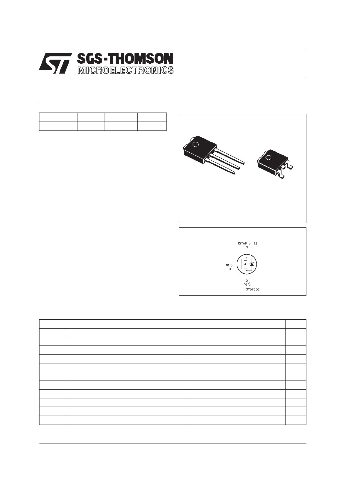
3
2
IPAK
TO-251
(Suffix”-1”)
1
(Suffix ”T4”)
1
DPAK
TO-252
INTERNAL SCHEMATIC DIAGRAM
3
ABSOLUTE MAXIMUM RATINGS
Symbol Parameter Value Unit
V
V
V
I
DM
P
dv/ dt(
T
(•) Pulse width limited by safe operatingarea (1)ISD≤ 40 A,di/dt ≤ 300 A/µs, VDD≤ V
(**) Value limited only by the package
December 1997
Drain-sourc e Vol t ag e (VGS=0) 30 V
DS
Drain- gate Voltag e (RGS=20kΩ)
DGR
Gate- source Voltage ± 15 V
GS
I
Drain Cur rent ( c on t in uous) at Tc=25oC 20** A
D
I
Drain Cur rent ( c on t in uous) at Tc=100oC 20** A
D
30 V
(•) Drain Current (pulsed) 100 A
Total Dissipation at Tc=25oC50W
tot
Derating F act or 0.33 W/
1) Peak Diode Recover y v olt ag e slope 7 V/ns
St orage Te mperatu re -65 to 175
stg
T
Max. Operat ing Junction T emperat ure 175
j
(BR)DSS,Tj≤TJMAX
o
C
o
C
o
C
1/9
Page 2
STD20NE03L
THERMAL DATA
R
thj-case
R
thj-amb
R
thc-sin k
T
AVALANCHE CHARACTERISTICS
Symbol Para met e r Max Value Uni t
I
AR
E
Ther mal Resist ance Junctio n-case Max
Ther mal Resist ance Junctio n-ambient Max
Ther mal Resist ance Case-sink Ty p
Maximum Lead T emperat ure For Soldering Purpose
l
Avalanche Current , Repet it ive or Not - Re petitive
(pulse width limited b y T
Single Pulse Avalanche Energy
AS
(starting T
=25oC, ID=IAR,VDD=25V)
j
max, δ <1%)
j
3
100
1.5
275
20 A
140 mJ
o
C/W
o
C/W
o
C/W
o
C
ELECTRICAL CHARACTERISTICS (T
=25oC unlessotherwise specified)
case
OFF
Symbol Parameter Test Cond itions Min. Typ. Max. Unit
V
(BR)DSS
Drain-sourc e
=250µAVGS=0
I
D
30 V
Breakdown Volt age
I
I
DSS
GSS
Zer o G at e Volt age
Drain Cur rent (V
GS
Gat e-body Le akage
Current (V
DS
=0)
=0)
=MaxRating
V
DS
V
=MaxRating Tc=125
DS
o
C
= ± 15 V
V
GS
1
10
± 100 nA
ON (∗)
Symbol Parameter Test Cond itions Min. Typ. Max. Unit
V
GS(th )
Gate Threshold
V
DS=VGSID
=250µA
11.82.5V
Voltage
R
DS(on)
I
D(on)
Stati c D rain-source On
Resistance
VGS=10V ID=10A
=5V ID=10A
V
GS
On St at e Dra in Cu rr e nt VDS>I
D(on)xRDS(on)max
0.016 0. 0 2
0.026ΩΩ
20 A
VGS=10V
DYNAMIC
Symbol Parameter Test Cond itions Min. Typ. Max. Unit
g
(∗)Forward
fs
Tr ansconductanc e
C
C
C
Input Capacit an c e
iss
Out put C apa c itance
oss
Reverse T ransf er
rss
Capa cit an c e
VDS>I
D(on)xRDS(on)maxID
=10A 12 18 S
VDS=25V f=1MHz VGS= 0 1850
450
160
2400
590
210
µA
µA
pF
pF
pF
2/9
Page 3
STD20NE03L
ELECTRICAL CHARACTERISTICS (continued)
SWITCHINGON
Symbol Parameter Test Cond itions Min. Typ. Max. Unit
t
d(on)
Q
Q
Q
Turn-on Tim e
Rise T ime
t
r
Total Gate Charge
g
Gat e-Sour ce Charge
gs
Gate-Drain Charge
gd
VDD=15V ID=20A
=4.7 Ω VGS=5V
R
G
VDD=24V ID=40A VGS=5V 29
SWITCHINGOFF
Symbol Parameter Test Cond itions Min. Typ. Max. Unit
t
r(Voff)
t
Of f - voltage Rise T ime
t
Fall Time
f
Cross-ov er Tim e
c
VDD=24V ID=40A
=4.7 Ω VGS=5V
R
G
SOURCE DRAIN DIODE
Symbol Parameter Test Cond itions Min. Typ. Max. Unit
I
SD
I
SDM
V
SD
t
Q
I
RRM
(∗) Pulsed: Pulse duration =300 µs, duty cycle1.5 %
(•) Pulse width limited by safe operating area
Source-drain Current
(•)
Source-drain Current
(pulsed)
(∗) Forwar d O n Volt age ISD=20A VGS=0 1.5 V
Reverse Rec overy
rr
Time
Reverse Rec overy
rr
= 40 A di/dt = 100 A/µs
I
SD
=20V Tj=150oC
V
DD
Charge
Reverse Rec overy
Current
25
16033210
38 nC
12
14
25
120
155
33
160
210
20
100
50
0.9
3.5
ns
ns
nC
nC
ns
ns
ns
A
A
ns
µC
A
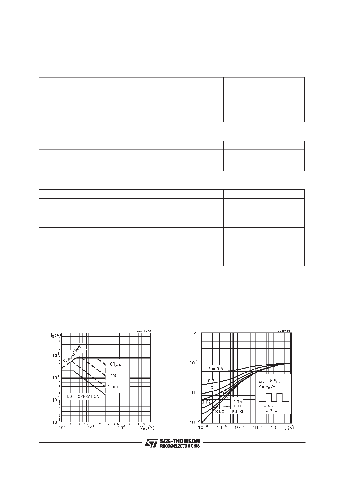
Safe Operating Area ThermalImpedance
3/9
Page 4

STD20NE03L
OutputCharacteristics
Transconductance
TransferCharacteristics
StaticDrain-sourceOn Resistance
GateCharge vs Gate-sourceVoltage
4/9
CapacitanceVariations
Page 5

STD20NE03L
Normalized GateThresholdVoltage vs
Temperature
Source-drainDiode Forward Characteristics
Normalized On Resistancevs Temperature
5/9
Page 6

STD20NE03L
Fig. 1: Unclamped Inductive Load Test Circuit
Fig. 3: SwitchingTimes Test Circuits For
ResistiveLoad
Fig. 2: Unclamped Inductive Waveform
Fig. 4: Gate Charge test Circuit
Fig. 5: Test Circuit For InductiveLoad Switching
And Diode RecoveryTimes
6/9
Page 7

TO-251 (IPAK) MECHANICAL DATA
STD20NE03L
DIM.
mm inch
MIN. TYP. MAX. MIN. TYP. MAX.
A 2.2 2.4 0.086 0.094
A1 0.9 1.1 0.035 0.043
A3 0.7 1.3 0.027 0.051
B 0.64 0.9 0.025 0.031
B2 5.2 5.4 0.204 0.212
B3 0.85 0.033
B5 0.3 0.012
B6 0.95 0.037
C 0.45 0.6 0.017 0.023
C2 0.48 0.6 0.019 0.023
D 6 6.2 0.236 0.244
E 6.4 6.6 0.252 0.260
G 4.4 4.6 0.173 0.181
H 15.9 16.3 0.626 0.641
L 9 9.4 0.354 0.370
L1 0.8 1.2 0.031 0.047
L2 0.8 1 0.031 0.039
A
E
==
C2
L2
B2
==
H
C
A3
A1
B6
L
B
B5
G
==
D
B3
2
13
L1
0068771-E
7/9
Page 8

STD20NE03L
TO-252 (DPAK) MECHANICAL DATA
DIM.
mm inch
MIN. TYP. MAX. MIN. TYP. MAX.
A 2.2 2.4 0.086 0.094
A1 0.9 1.1 0.035 0.043
A2 0.03 0.23 0.001 0.009
B 0.64 0.9 0.025 0.035
B2 5.2 5.4 0.204 0.212
C 0.45 0.6 0.017 0.023
C2 0.48 0.6 0.019 0.023
D 6 6.2 0.236 0.244
E 6.4 6.6 0.252 0.260
G 4.4 4.6 0.173 0.181
H 9.35 10.1 0.368 0.397
L2 0.8 0.031
L4 0.6 1 0.023 0.039
8/9
H
A
E
==
C2
L2
B2
==
DETAIL”A”
D
2
13
L4
A1
C
A2
DETAIL”A”
B
G
==
0068772-B
Page 9

STD20NE03L
Information furnished is believed to be accurateand reliable. However, SGS-THOMSONMicroelectronics assumes no responsability for the
consequencesof use ofsuch information nor for anyinfringement of patentsor otherrights of third parties whichmay results from its use. No
licenseis granted by implicationor otherwise underany patentor patent rightsof SGS-THOMSON Microelectronics.Specificationsmentioned
in this publicationare subject to change without notice.This publication supersedes and replaces all informationpreviously supplied.
SGS-THOMSONMicroelectronics productsare notauthorized for useas criticalcomponents in lifesupportdevicesor systems withoutexpress
writtenapproval of SGS-THOMSONMicroelectonics.
1997 SGS-THOMSONMicroelectronics- Printed in Italy - AllRights Reserved
Australia- Brazil - Canada- China- France- Germany - Italy - Japan - Korea - Malaysia - Malta- Morocco - The Netherlands -
Singapore- Spain- Sweden- Switzerland- Taiwan - Thailand - United Kingdom- U.S.A
SGS-THOMSONMicroelectronics GROUP OF COMPANIES
...
9/9
 Loading...