

Datasheet STP2NC70ZFP, STP2NC70Z, STD1NC70Z-1, STD1NC70Z Datasheet (SGS Thomson Microelectronics)
Page 1
STP2NC70Z , STP 2NC70 Z FP
STD1NC70Z, STD1NC70Z-1
N-CH A NNEL 700V - 7.3Ω - 1.4A TO-220/FP/DPAK/IPAK
Zener-Protected PowerMESH™III MOSFET
TYPE V
STP2NC70Z
STP2NC70ZFP
STD1NC70Z
STD1NC70Z-1
■ TYPICAL R
■ EXTREMELY HIGH dv /d t CAPABILITY
■ 100% AVALANCHE TESTED
■ GATE CHARGE MINIMIZED
■ VERY LOW INTRINSIC CAPAC ITANCES
700 V
700 V
700 V
700 V
(on) = 7.3 Ω
DS
DSS
R
DS(on)
< 8.5 Ω
< 8.5 Ω
< 8.5 Ω
< 8.5 Ω
I
D
1.4 A
1.4 A
1.4 A
1.4 A
Pw
50 W
25 W
45 W
45 W
DESCRIPTION
The third generation of MESH O VERLAY™ Power
MOSFETs for very high voltage exhibits unsurpassed on-resistance per unit area while integrating
back-to-back Zener diodes between gate and
source. Such arrangement gives extra ESD capability with higher ruggedness performance as requested by a large variety of single-switch applications..
APPLICATIONS
■ SINGLE-ENDED SMPS IN MONITORS,
COMPUTER AND INDUSTRIAL APPLICATION
■ WELDING EQUIPMENT
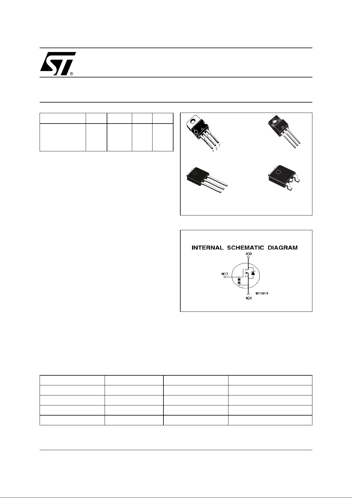
TO-220
IPAK
3
2
1
TO-220FP
3
2
1
DPAK
3
1
ORDERING INFORMATION
SALES TYPE MARKING PACKAGE PACKAGING
STP2NC70Z P2NC70Z TO-220 TUBE
STP2NC70ZFP P2NC70ZFP TO-220FP TUBE
STD1NC70ZT4 D1NC70Z DPAK TAPE & REEL
STD1NC70Z-1 D1NC70Z IPAK TUBE
1/13February 2002
Page 2
STP2NC70Z, STP2NC70ZFP, STD1NC70Z, STD1NC70Z-1
ABSOLUTE MAXIMUM RATINGS
Symbol Parameter Value Unit
STP2NC70Z STP2NC70ZFP
V
I
V
V
DM
P
DS
DGR
GS
I
D
I
D
TOT
Drain-source Voltage (VGS = 0)
Drain-gate Voltage (RGS = 20 kΩ)
700 V
700 V
Gate- source Voltage ± 25 V
Drain Current (continuos) at TC = 25°C
Drain Current (continuos) at TC = 100°C
(l)
Drain Current (pulsed) 5.6 5.6 (*) 5.6 A
Total Dissipation at TC = 25°C
1.4 1.4 (*) 1.4 A
0.9 0.9 (*) 0.9 A
50 25 45 W
Derating Factor 0.4 0.2 0.36 W/°C
I
GS
V
ESD(G-S)
Gate-source Current (DC) ± 50 mA
Gate source ESD(HBM-C=100pF, R=1.5KΩ) 2000 V
dv/dt (1) Peak Diode Recovery voltage slope 3 V/ns
V
ISO
T
j
T
stg
(l) Pulse wi dth limited by safe operating area
(1) I
≤10A, di/dt ≤200A/µs, VDD ≤ V
SD
(*) Limited only by maximum temperature allowed
Insulation Withstand Voltage (DC) - 2500 - V
Operating Junction Temperature
Storage Temperature
, Tj ≤ T
(BR)DSS
JMAX.
-65 to 150
-65 to 150
STD1NC70Z
STD1NC70Z-1
°C
°C
THERMA L D ATA
TO-220 TO-220FP
Rthj-case Thermal Resistance Junction-case Max 2.5 5 2.75 °C/W
Rthj-pcb Thermal Resistance Junction-pcb Max (for SMD) (#) 100 °C/W
Rthj-amb Thermal Resistance Junction-ambient Max 62.5 100 °C/W
T
l
Maximum Lead Temperature For Soldering Purpose
300
DPAK
IPAK
275
°C
AVALANCHE CHARACTERISTICS
Symbol Par amet er Max Value Unit
I
AR
E
AS
Avalanche Current, Repetitive or Not-Repetitive
(pulse width limited by T
max)
j
Single Pulse Avalanche Energy
(starting T
= 25 °C, ID = IAR, VDD = 50 V)
j
1.4 A
60 mJ
GATE-SOURCE ZENER DIODE
Symbol Parameter Test Conditions Min. Typ. Max. Unit
BV
GSO
Gate-Source Breakdown
Igs=± 1mA (Open Drain) 25 V
Voltage
αT Voltage Thermal Coefficient T=25°C Note(3) 1.3
Note : 3 . ∆V
(#) When mounted on minimum Footprint
= αT (25°-T) BV
BV
GSO
(25°)
10
-4
/°C
PROTECTION FEATURES OF GATE-TO-SOURCE ZENER DIODES
The built-in back-to-back Zener diodes have specifically been designed to enhance not only the device’s
ESD capability, but also to make them safely absorb possible voltage transients that may occasionally be
applied from gate to souce. In this respect the Zener voltage is appropriate to achieve an efficient and costeffective intervention to protect the device’s integrity. These integrated Zener diodes thus avoid the usage
of external components.
2/13
Page 3
STP2NC70Z, STP2NC70ZFP, STD1NC70Z, STD1NC70Z-1
ELECTRICAL CHARACTERISTICS (TCASE =25°C UNLESS OTHERWISE SPECIFIED)
ON/OFF
Symbol Parameter Test Conditions Min. Typ. Max. Unit
V
(BR)DSS
Drain-source
Breakdown Voltage
I
DSS
I
GSS
V
GS(th)
R
DS(on)
Zero Gate Voltage
Drain Current (V
GS
= 0)
Gate-body Leakage
Current (V
DS
= 0)
Gate Threshold Voltage
Static Drain-source On
Resistance
DYNAMIC
Symbol Parameter Test Conditions Min. Typ. Max. Unit
g
(1) Forward Transconductance VDS = 15 V, ID= 0.7 A 1.2 S
fs
C
oss eq.
C
iss
C
oss
C
rss
Input Capacitance
Output Capacitance
Reverse Transfer
Capacitance
(3) Equivalent Output
Capacitance
SWITCHING ON
Symbol Parameter Test Conditions Min. Typ. Max. Unit
t
d(on)
Q
Q
Q
t
r
gs
gd
Turn-on Delay Time
Rise Time
Total Gate Charge
g
Gate-Source Charge
Gate-Drain Charge
ID = 250 µA, VGS = 0 700 V
V
= Max Rating
DS
VDS = Max Rating, TC = 125 °C
V
= ± 20V ±10 µA
GS
V
= VGS, ID = 250µA
DS
345V
1
50
VGS = 10V, ID = 0.7 A 7.3 8.5 Ω
= 25V, f = 1 MHz, VGS = 0 305
V
DS
34
3.6
VGS = 0V, VDS = 0V to 560V 28 pF
VDD = 350 V, ID = 0.8 A
RG= 4.7Ω VGS = 10 V
11
8
(Resistive Load see, Figure 3)
= 560V, ID = 1.6 A,
V
DD
VGS = 10V
8
2
12
3.8
µA
µA
pF
pF
pF
ns
ns
nC
nC
nC
SWITCHING OFF
Symbol Parameter Test Conditions Min. Typ. Max. Unit
t
d(off)
Turn-off Delay Time
t
f
Fall Time
VDD = 350 V, ID = 0.8 A
RG=4.7Ω VGS = 10 V
27
30
(Resistive Load see, Figure 3)
t
r(Voff)
t
t
= 560V, ID = 1.6 A,
Off-voltage Rise Time
f
c
Fall Time
Cross-over Time
V
DD
RG=4.7Ω, V
GS
= 10V
(Inductive Load see, Figure 5)
20
5
25
SOURCE DRAIN DIODE
Symbol Parameter Test Conditions Min. Typ. Max. Unit
I
SD
I
SDM
VSD (1)
t
rr
Q
rr
I
RRM
Note: 1. Pulsed: Pu l se duration = 300 µs, duty c ycle 1.5 %.
2. Pulse width li mited by safe operating area.
3. C
Source-drain Current
(2)
Source-drain Current (pulsed)
Forward On Voltage
Reverse Recovery Time
Reverse Recovery Charge
Reverse Recovery Current
is defined as a constant equivalent capacitance giving the same charging time as C
oss eq.
V
.
DSS
ISD = 1.4 A, VGS = 0
ISD = 1.6 A, di/dt = 100A/µs
V
DD
(see test circuit, Figure 5)
= 30V, Tj = 150°C
370
1.3
6.8
when VDS increase s fr om 0 to 80%
oss
1.4
5.6
1.6 V
ns
ns
ns
ns
ns
A
A
ns
µC
A
3/13
Page 4
STP2NC70Z, STP2NC70ZFP, STD1NC70Z, STD1NC70Z-1
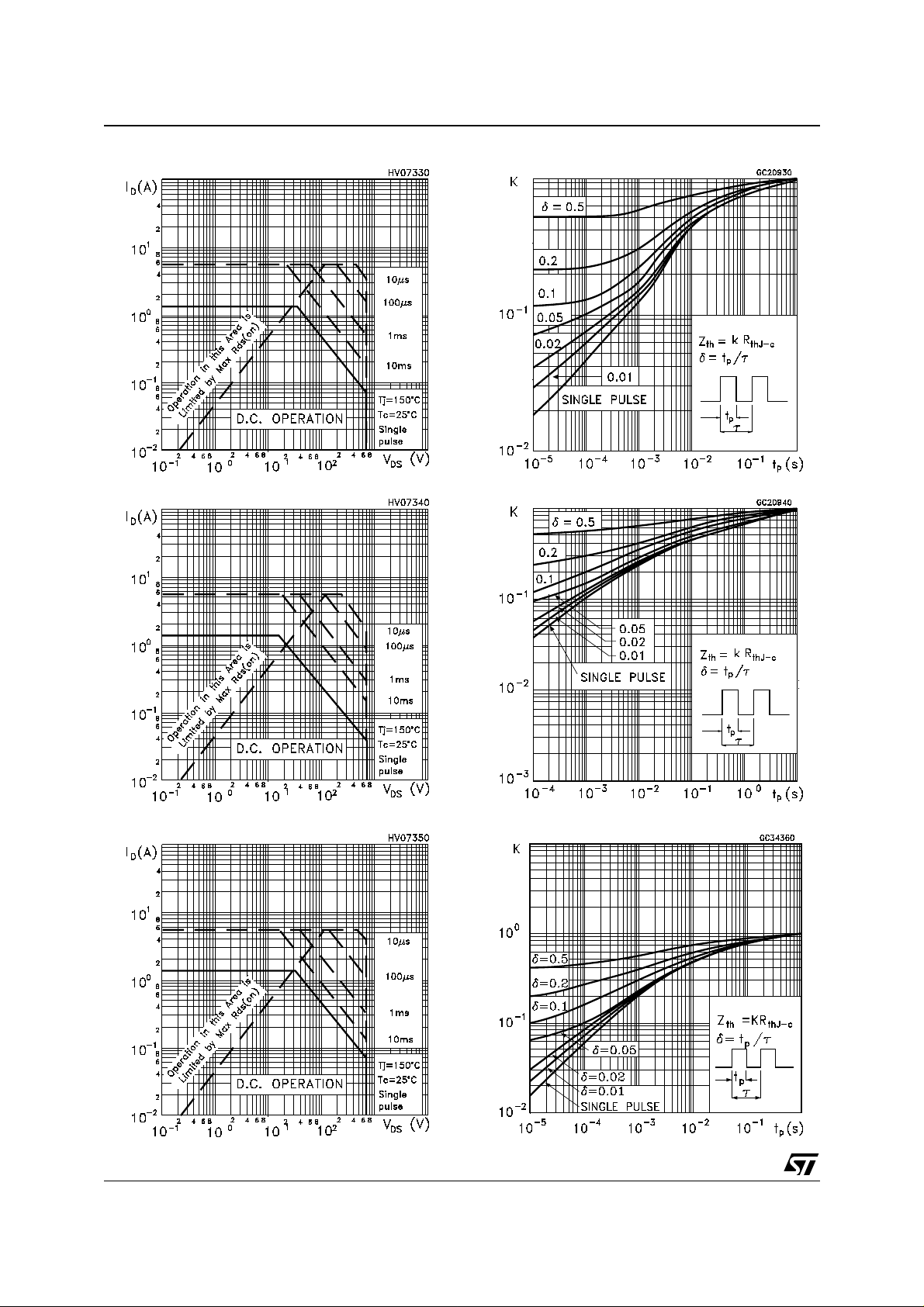
Safe Operating Area For TO-220 Thermal Impedance For TO-220
Safe Operating Area For TO-220FP
Safe Operating Area For DPAK/IPAK Thermal Impedance For DPAK/IPAK
Thermal Impedance For TO-220FP
4/13
Page 5

STP2NC70Z, STP2NC70ZFP, STD1NC70Z, STD1NC70Z-1
Output Characteristics
Transconductance
Transfer Characteristics
Static Drain-source On Resistance
Gate Charge vs Gate-source Voltage Capacitance Variations
5/13
Page 6

STP2NC70Z, STP2NC70ZFP, STD1NC70Z, STD1NC70Z-1
Normalized Gate Threshold Volta ge vs Temp.
Source-drain Diode Forward Characteristics
Normalized On Resistance vs Temperatur e
Normalized BVDSS vs Temperature
6/13
Page 7

STP2NC70Z, STP2NC70ZFP, STD1NC70Z, STD1NC70Z-1
Fig. 2: Unclamped Inductive WaveformFig. 1: Unclamped Inductive Load Test Circuit
Fig. 3: Switching Times Test Circuit For
Resistive Load
Fig. 5: Test Circuit For Inductive Load Switching
And Diode Recovery Times
Fig. 4: Gate Charge test Circuit
7/13
Page 8

STP2NC70Z, STP2NC70ZFP, STD1NC70Z, STD1NC70Z-1
E
TO-220 MECHANICAL DATA
DIM.
A 4.40 4.60 0.173 0.181
C 1.23 1.32 0.048 0.051
D 2.40 2.72 0.094 0.107
D1 1.27 0.050
E 0.49 0.70 0.019 0.027
F 0.61 0.88 0.024 0.034
F1 1.14 1.70 0.044 0.067
F2 1.14 1.70 0.044 0.067
G 4.95 5.15 0.194 0.203
G1 2.4 2.7 0.094 0.106
H2 10.0 10.40 0.393 0.409
L2 16.4 0.645
L4 13.0 14.0 0.511 0.551
L5 2.65 2.95 0.104 0.116
L6 15.25 15.75 0.600 0.620
L7 6.2 6.6 0.244 0.260
L9 3.5 3.93 0.137 0.154
DIA. 3.75 3.85 0.147 0.151
MIN. TYP . MAX. MIN. TY P . MAX.
mm inch
A
C
D
8/13
L5
Dia.
L7
D1
L6
L2
L9
F1
G1
F
H2
G
F2
L4
P011C
Page 9

STP2NC70Z, STP2NC70ZFP, STD1NC70Z, STD1NC70Z-1
TO-220FP MECHANICAL DATA
DIM.
MIN. TYP. MAX. MIN. TYP. MAX.
A 4.4 4.6 0.173 0.181
B 2.5 2.7 0.098 0.106
D 2.5 2.75 0.098 0.108
E 0.45 0.7 0.017 0.027
F 0.75 1 0.030 0.039
F1 1.15 1.7 0.045 0.067
F2 1.15 1.7 0.045 0.067
G 4.95 5.2 0.195 0.204
G1 2.4 2.7 0.094 0.106
H 10 10.4 0.393 0.409
L2 16 0.630
L3 28.6 30.6 1.126 1.204
L4 9.8 10.6 0.385 0.417
L6 15.9 16.4 0.626 0.645
L7 9 9.3 0.354 0.366
Ø 3 3.2 0.118 0.126
mm inch
E
A
D
B
L3
L6
L7
¯
F1
F
G1
H
G
F2
123
L2
L4
9/13
Page 10

STP2NC70Z, STP2NC70ZFP, STD1NC70Z, STD1NC70Z-1
TO-251 (IPAK) MECHANICAL DAT A
DIM.
MIN. TYP. MAX. MIN. TYP. MAX.
mm inch
A 2.2 2.4 0.086 0.094
A1 0.9 1.1 0.035 0.043
A3 0.7 1.3 0.027 0.051
B 0.64 0.9 0.025 0.031
B2 5.2 5.4 0.204 0.212
B3 0.85 0.033
B5 0.3 0.012
B6 0.95 0.037
C 0.45 0.6 0.017 0.023
C2 0.48 0.6 0.019 0.023
D 6 6.2 0.236 0.244
E 6.4 6.6 0.252 0.260
G 4.4 4.6 0.173 0.181
H 15.9 16.3 0.626 0.641
L 9 9.4 0.354 0.370
L1 0.8 1.2 0.031 0.047
L2 0.8 1 0.031 0.039
H
10/13
A
C2
L2
E
B2
= =
= =
D
B3
2
1 3
L1
A1
L
B6
C
A3
B
B5
G
= =
0068771-E
Page 11

STP2NC70Z, STP2NC70ZFP, STD1NC70Z, STD1NC70Z-1
TO-252 (DPAK) MECHANICAL DATA
DIM.
A 2.20 2.40 0.087 0.094
A1 0.90 1.10 0.035 0.043
A2 0.03 0.23 0.001 0.009
B 0.64 0.90 0.025 0.035
B2 5.20 5.40 0.204 0.213
C 0.45 0.60 0.018 0.024
C2 0.48 0.60 0.019 0.024
D 6.00 6.20 0.236 0.244
E 6.40 6.60 0.252 0.260
G 4.40 4.60 0.173 0.181
H 9.35 10.10 0.368 0.398
L2 0.8 0.031
L4 0.60 1.00 0.024 0.039
V2 0
MIN. TYP. MAX. MIN. TYP. MAX.
o
mm inch
o
8
o
0
o
0
P032P_B
11/13
Page 12

STP2NC70Z, STP2NC70ZFP, STD1NC70Z, STD1NC70Z-1
DPAK FOOTPRINT
All dimensions are in millimeters
TAPE AND REEL SHIPMENT (suffix ”T4”)*
TUBE SHIPMENT (no suffix)*
All dimensions
are in millimeters
REEL MECHANICAL DATA
DIM.
A 330 12.992
B 1.5 0 .059
C 12.8 13.2 0.504 0.520
D 20.2 0.795
G 16.4 18.4 0.645 0.724
N 50 1.968
T 22.4 0. 881
mm inch
MIN. MAX. MIN. MAX.
TAPE MECHANICAL DATA
DIM.
A0 6.8 7 0.267 0.275
B0 10.4 10.6 0.409 0.417
B1 12.1 0.476
D 1.5 1.6 0.059 0.063
D1 1.5 0.059
E 1.65 1.85 0.065 0.073
F 7.4 7.6 0.291 0.299
K0 2.55 2.75 0.100 0.108
P0 3.9 4.1 0.153 0.161
P1 7.9 8.1 0.311 0.319
P2 1.9 2.1 0.075 0.082
R 40 1.574
W 15.7 16.3 0.618 0.641
* on sales type
12/13
mm inch
MIN. MAX. MIN. MAX.
BASE QTY BULK QTY
2500 2500
Page 13

STP2NC70Z, STP2NC70ZFP, STD1NC70Z, STD1NC70Z-1
Information furnished is believed to be accurate and reliable. However, STMicroelectronics assumes no responsibility for the consequences
of use of such informa tion n or for an y infring ement of patent s or other rig hts of third part ies which may resu lt from its use . No l i cen se i s
granted by implication or otherwise under any patent or patent rights of STMicroelectronics. Specification mentioned in this publication are
subject to change without notice. This publication supersedes and replaces all information previously supplied. STMicroelectronics products
are not authorized for use as critical compo nents in life support devices or systems without express written approval of STMicroelectronics.
Australia - Brazil - China - Finland - France - Germany - Hong Kong - India - Italy - Japan - Malaysia - Malta - Morocco -
The ST logo is a trademark of STMicroelectronics
© 2000 STMicroelectronics – Printed in Italy – All Rights Reserved
STMicroelectronics GROUP OF COMPANIES
Singapore - Spain - Sweden - Switzerland - United Kingdom - U.S.A.
http://www.st.com
13/13
 Loading...