

Page 1
STB7NA40
N - CHANNEL ENHANCEMENT MODE
FAST POWER MOS TRANSISTOR
TYPICALR
DS(on)
= 0.82 Ω
± 30V GATE TOSOURCE VOLTAGE RATING
100% AVALANCHETESTED
REPETITIVEAVALANCHEDATAAT100
o
C
LOW INTRINSIC CAPACITANCES
GATECHARGE MINIMIZED
REDUCEDTHRESHOLD VOLTAGESPREAD
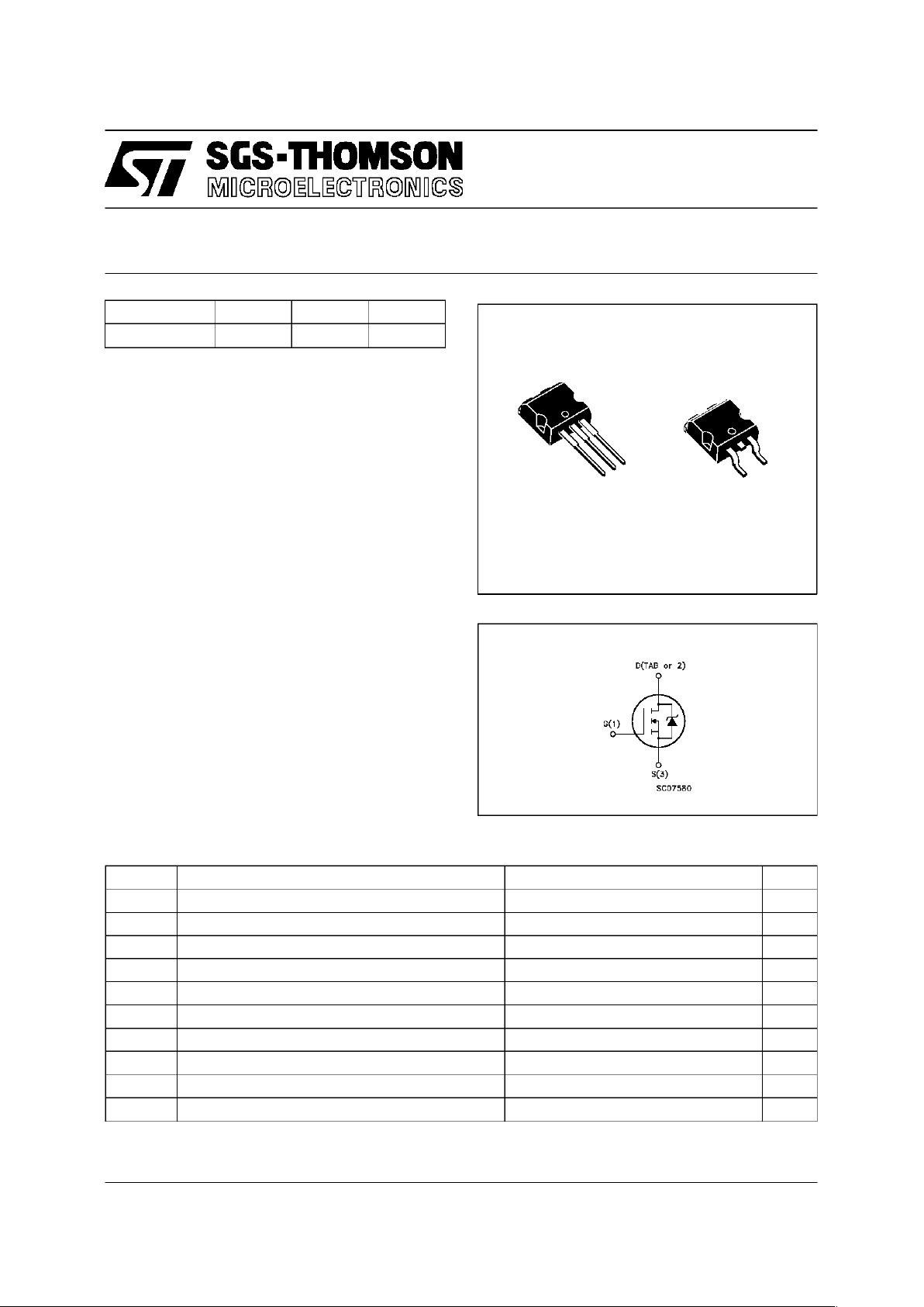
THROUGH-HOLEI2PAK (TO-262) POWER
PACKAGEIN TUBE(SUFFIX ”-1”)
SURFACE-MOUNTING D2PACK (TO-263)
POWERPACKAGEIN TUBE(NO SUFFIX)
OR IN TAPE & REEL (SUFFIX ”T4”)
APPLICATIONS
HIGH CURRENT, HIGH SPEED SWITCHING
SWITCHMODE POWER SUPPLIES(SMPS)
DC-AC CONVERTERSFOR WELDING
EQUIPMENTANDUNINTERRUPTIBLE
POWERSUPPLIESAND MOTOR DRIVE
INTERNAL SCHEMATIC DIAGRAM
ABSOLUTE MAXIMUM RATINGS
Symbol Parameter Val ue Uni t
V
DS
Drain-source Voltage (VGS= 0) 400 V
V
DGR
Drain- gate Voltage ( RGS=20kΩ) 400 V
V
GS
Gate-s ource Voltage ± 30 V
I
D
Drain Current (continuous) at Tc=25oC6.5A
I
D
Drain Current (continuous) at Tc=100oC4.1A
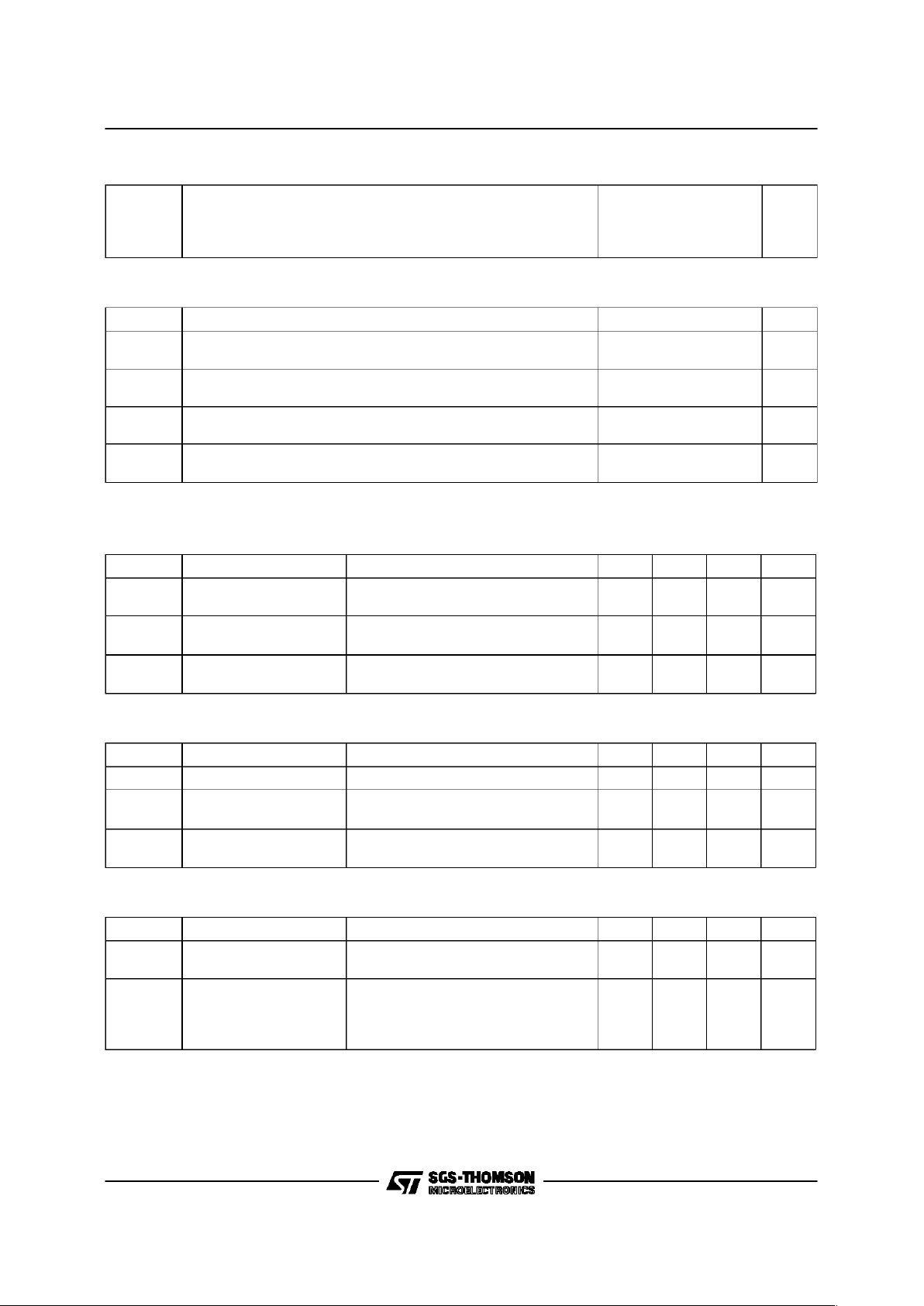
I
DM
(•) Drain Current (pulsed) 26 A
P
tot
Tot al Dissipat ion at Tc=25oC 100 W
Derat ing Fa ct or 0.8 W/
o
C
T
stg
Sto rage Tem perature -65 t o 15 0
o
C
T
j
Max. Operat ing Juncti on Temper at u r e 150
o
C
(•) Pulsewidth limitedby safe operating area
TYPE V
DSS
R
DS(on )
I
D
STB 7NA40 400 V < 1 Ω 6.5 A
October 1995
1
2
3
1
3
I2PAK
TO-262
D2PAK
TO-263
1/10
Page 2
THERMAL DATA
R
thj-case
R
thj-amb
R
thc-sink
T
l
Therm al Resistanc e Juncti on-c ase Max
Therm al Resistanc e Juncti on-am b ient Max
Therm al Resistanc e Case-sink Ty p
Maxim um Lead Tem p era t ure For So ldering Purpose
1.25
62.5
0.5
300
o
C/W
o
C/W
o
C/W
o
C
AVALANCHE CHARACTERISTICS
Symb ol Param et er Max V al ue Uni t
I
AR
Avalanc h e Current , Repet it ive or Not -Repetiti ve
(pulse width limited by T
j
max, δ <1%)
6.5 A
E
AS
Single Pulse Avalanche Energy
(starting T
j
=25oC, ID=IAR,VDD=50V)
210 mJ
E
AR
Repetit ive Avalanche Energy
(pulse width limited by T
j
max, δ <1%)
8.4 mJ
I
AR
Avalanc h e Current , Repet it ive or Not -Repetiti ve
(T
c
=100oC, pulse wi dt h limited by Tjmax, δ <1%)
4.1 A
ELECTRICAL CHARACTERISTICS (T
case
=25oC unlessotherwise specified)
OFF
Symb ol Par amete r Test Cond i ti ons Min. Typ . Max. Uni t
V
(BR)DSS
Drain-s ource
Break down Vol t age
ID= 250 µ AVGS=0 400 V
I
DSS
Zero G ate Voltage
Drain Current (V
GS
=0)
V
DS
= Max Rating
V
DS
= Max Rating x 0.8 Tc=125oC
250
1000µAµA
I
GSS
Gat e- body Leakage
Current (V
DS
=0)
V
GS
= ± 30 V ± 100 nA
ON (∗)
Symb ol Par amete r Test Cond i ti ons Min. Typ . Max. Uni t
V
GS(t h)
Gat e T hreshold Voltage VDS=VGSID= 250 µA 2.25 3 3.75 V
R
DS(on)
Sta t ic Drain-sour ce O n
Resistance
VGS= 10V ID=3.5A
V
GS
=10V ID=3.5A Tc= 100oC
0.82 1
2
Ω
Ω
I
D(on)
On S t ate Drain Current VDS>I
D(on)xRDS(on)max
VGS=10V
6.5 A
DYNAMIC
Symb ol Par amete r Test Cond i ti ons Min. Typ . Max. Uni t
g
fs
(∗)Forward
Tra nsconductanc e
VDS>I
D(on)xRDS(on)maxID
= 3.5 A 3.1 4.6 S
C
iss
C
oss
C
rss
Input Capacitance
Out put Capacitanc e
Reverse Transfer
Capacit an c e
VDS=25V f=1MHz VGS= 0 700
120
31
900
160
43
pF
pF
pF
STB7NA40
2/10
Page 3
ELECTRICAL CHARACTERISTICS (continued)
SWITCHING ON
Symb ol Par amete r Test Cond i ti ons Min. Typ . Max. Uni t
t
d(on)
t
r
Turn-on Time
Rise Time
VDD= 200 V ID=3.5A
R
G
=47 Ω VGS=10V
(see tes t circuit, figure 3)
25
75
35
100
ns
ns
(di/dt)
on
Turn-on Current Slope VDD= 320 V ID=7A
R
G
=47 Ω VGS=10V
(see tes t circuit, f igure 5)
220 A/µs
Q
g
Q
gs
Q
gd
Total Ga te Charge
Gat e- Source C har ge
Gate-Drain Charge
VDD=320V ID=7A VGS=10V 34
7
15
45 nC
nC
nC
SWITCHING OFF
Symb ol Par amete r Test Cond i ti ons Min. Typ . Max. Uni t
t
r(Voff)
t
f
t
c
Off-volt ag e Rise Time
Fall Time
Cross-over Time
VDD= 320 V ID=7A
R
G
=47 Ω VGS=10V
(see tes t circuit, figure 5)
40
25
75
55
35
100
ns
ns
ns
SOURCEDRAIN DIODE
Symb ol Par amete r Test Cond i ti ons Min. Typ . Max. Uni t
I
SD
I
SDM
(•)
Source-drain C urr ent
Source-drain C urr ent
(pulsed)
6.5
26
A
A
V
SD
(∗) For ward On Voltage ISD=6.5A VGS=0 1.6 V
t
rr
Q
rr
I
RRM
Revers e Recovery
Time
Revers e Recovery
Charge
Revers e Recovery
Current
ISD= 7 A di/dt = 100 A/µs
V
DD
=100V Tj=150oC
(see tes t circuit, figure 5)
380
4.8
25
ns
µC
A
(∗) Pulsed: Pulse duration =300 µs,duty cycle 1.5 %
(•) Pulse widthlimitedby safeoperating area
Safe Operating Area ThermalImpedance
STB7NA40
3/10
Page 4
Derating Curve
TransferCharacteristics
Static Drain-sourceOn Resistance
Output Characteristics
Transconductance
Gate Charge vs Gate-source Voltage
STB7NA40
4/10
Page 5
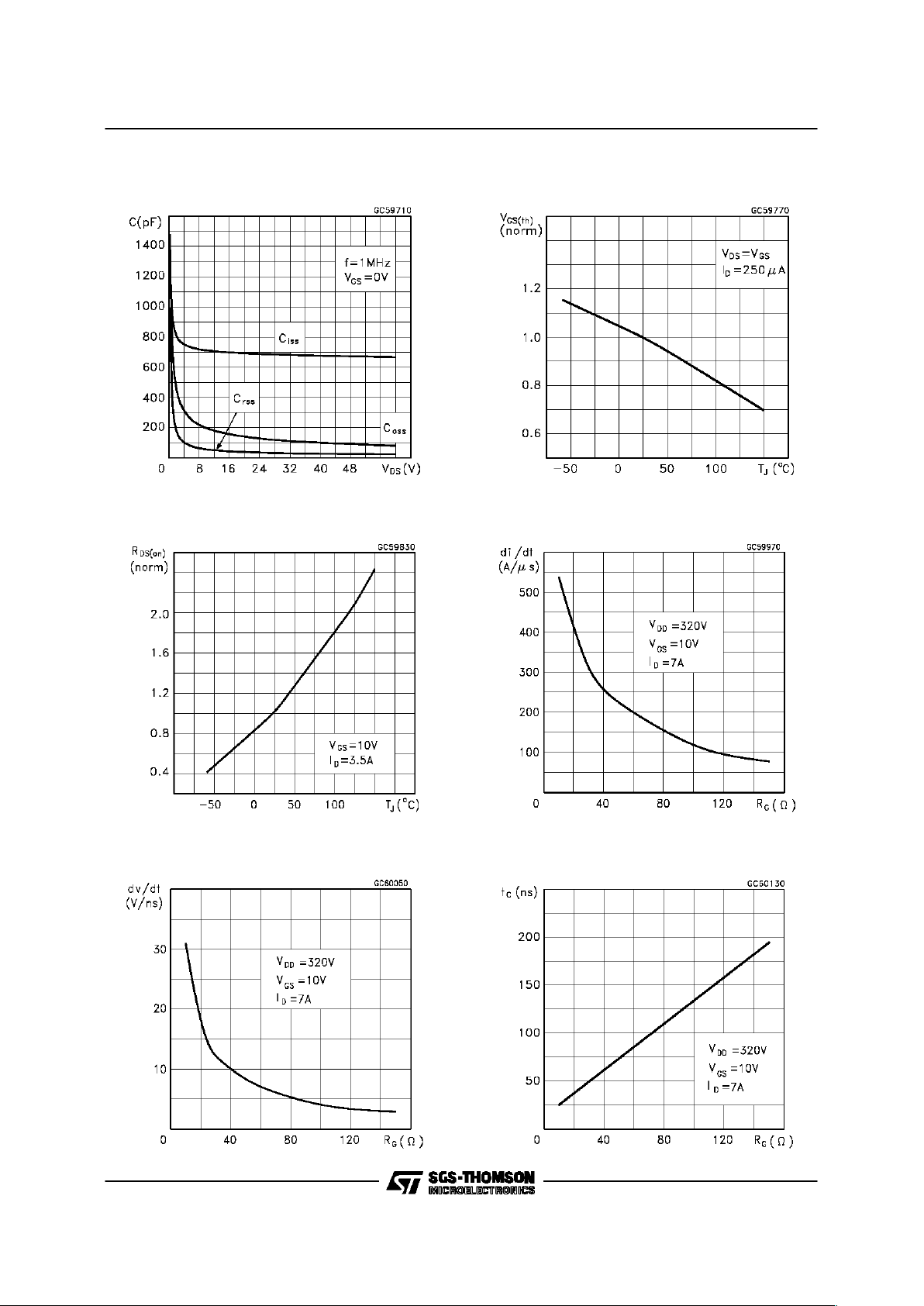
CapacitanceVariations
NormalizedOn Resistance vs Temperature
Turn-offDrain-source VoltageSlope
NormalizedGate Threshold Voltage vs
Temperature
Turn-onCurrent Slope
Cross-overTime
STB7NA40
5/10
Page 6

SwitchingSafe OperatingArea
Source-drainDiode Forward Characteristics
Fig. 1: UnclampedInductive Load Test Circuit
AccidentalOverload Area
Fig. 2: Unclamped Inductive Waveform
STB7NA40
6/10
Page 7
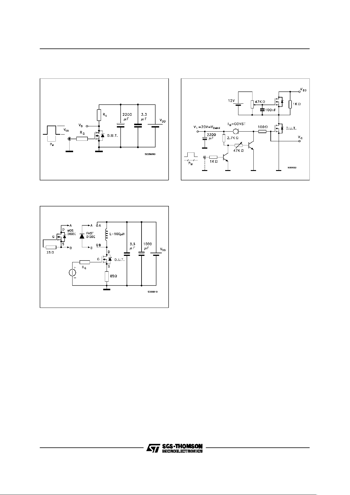
Fig. 3: SwitchingTimes Test Circuits For
ResistiveLoad
Fig. 5: TestCircuit For InductiveLoad Switching
And DIodeRecoveryTimes
Fig. 4: GateCharge test Circuit
STB7NA40
7/10
Page 8

DIM.
mm inch
MIN. TYP. MAX. MIN. TYP. MAX.
A 4.3 4.6 0.169 0.181
A1 2.49 2.69 0.098 0.106
B 0.7 0.93 0.027 0.036
B1 1.2 1.38 0.047 0.054
B2 1.25 1.4 0.049 0.055
C 0.45 0.6 0.017 0.023
C2 1.21 1.36 0.047 0.053
D 9 9.35 0.354 0.368
e 2.44 2.64 0.096 0.104
E 10 10.28 0.393 0.404
L 13.2 13.5 0.519 0.531
L1 3.48 3.78 0.137 0.149
L2 1.27 1.37 0.050 0.054
L
L1
B2
B
D
E
A
C2
C
A1
L2
e
TO-262 (I2PAK) MECHANICAL DATA
STB7NA40
8/10
Page 9

DIM.
mm inch
MIN. TYP. MAX. MIN. TYP. MAX.
A 4.3 4.6 0.169 0.181
A1 2.49 2.69 0.098 0.106
B 0.7 0.93 0.027 0.036
B2 1.25 1.4 0.049 0.055
C 0.45 0.6 0.017 0.023
C2 1.21 1.36 0.047 0.053
D 9 9.35 0.354 0.368
E 10 10.28 0.393 0.404
G 4.88 5.28 0.192 0.208
L 15 15.85 0.590 0.624
L2 1.27 1.37 0.050 0.054
L3 1.4 1.75 0.055 0.068
L2
L3
L
B2
B
G
E
A
C2
D
C
A1
TO-263 (D2PAK) MECHANICAL DATA
STB7NA40
9/10
Page 10

Information furnished is believed to be accurateand reliable. However,SGS-THOMSON Microelectronics assumes no responsability for the
consequences of use of such information nor forany infringement ofpatents orother rights of thirdparties which may results fromits use. No
licenseis granted by implication orotherwise underany patent or patentrights of SGS-THOMSONMicroelectronics. Specifications mentioned
in this publicationare subjectto change without notice.This publication supersedes andreplaces all informationpreviously supplied.
SGS-THOMSON Microelectronicsproductsarenotauthorized foruse as criticalcomponents in lifesupportdevices or systems without express
writtenapproval of SGS-THOMSONMicroelectonics.
1995 SGS-THOMSONMicroelectronics - All RightsReserved
SGS-THOMSONMicroelectronics GROUPOF COMPANIES
Australia- Brazil- France - Germany - Hong Kong -Italy - Japan- Korea - Malaysia - Malta - Morocco - The Netherlands-
Singapore- Spain- Sweden - Switzerland- Taiwan - Thailand- United Kingdom- U.S.A
...
STB7NA40
10/10
 Loading...