

Page 1
N - CHANNEL 30V - 0.008Ω - 70A D2PAK
STripFET
MAIN PRODUCT CHARACTERISTICS
MOSFET
SCHOTTKY
DESCRIPTION:
This product associat es a P owe r MOSFET of t he
third generati on of ST Mic roelectronics unique
”Single Featu r e S ize” stri p- based process and a
low drop S chottky diode. The transis tor shows the
best tra de-off between on-r esis tance and gate
charge. Used as low s ide in buck regulators, the
product is the bes t solution in t erm s of cond uc tion
losses and space saving.
MOSFET PLUS SCHOTTKY RECTIFIER
V
DSS
30V <0.01 Ω 70A
I
F(AV)
3A 30V 0.51V
R
DS(on)
V
RRM
V
F(MAX)
I
D
STB70NFS03L
PRELIMINARY DATA
3
1
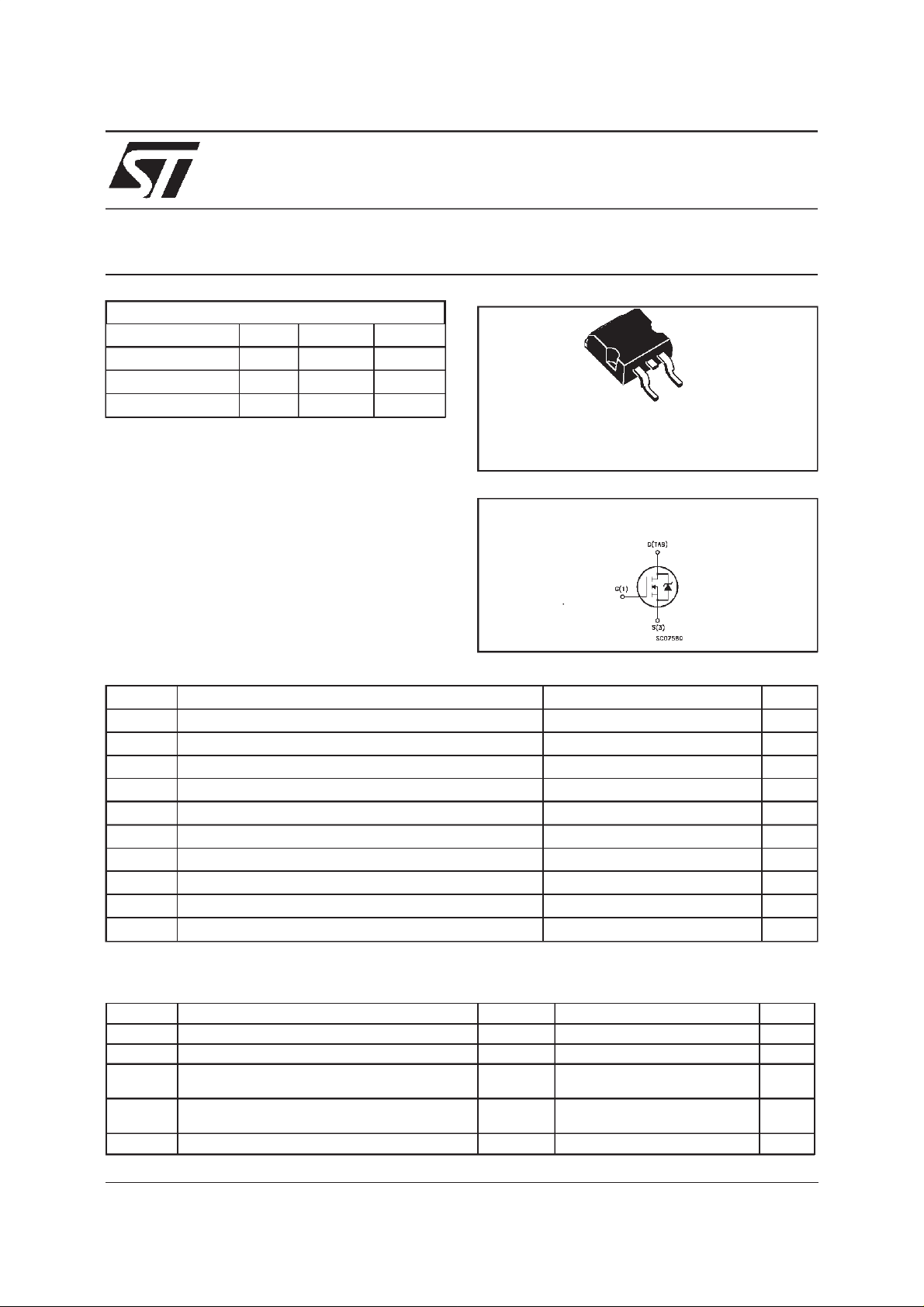
D2PAK
TO-263
(suffix ”T4”)
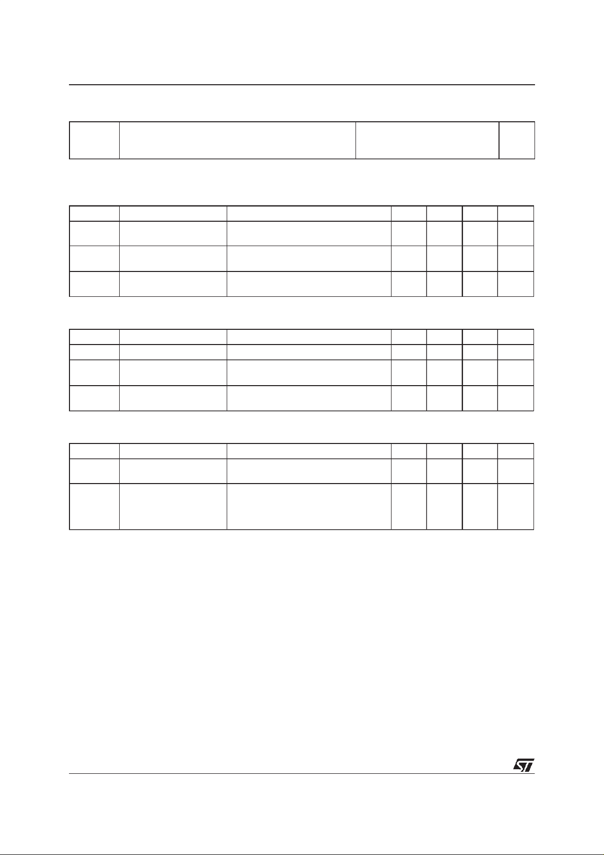
INTERNAL SCHEMATIC DIAGRAM
MOSFETABSOLUTE MAXIMUM RATINGS
Symbol Parameter Value Unit
V
V
V
I
DM
P
Drain-source Voltage (VGS=0) 30 V
DS
Drain- gate Volta ge (RGS=20kΩ)30V
DGR
Gat e- sour c e Volt age ± 22 V
GS
I
Drain Curre nt (cont i nuous) at Tc=25oC70A
D
I
Drain Curre nt (cont i nuous) at Tc= 100oC50A
D
(•) Drain Curre nt (pulse d) 280 A
Tot al Dissipat ion at Tc=25oC 100 W
tot
Derat ing F actor 0.67 W/
T
(•) Pulse width limited by safe operating area
Stora ge Tem pe ra tur e -65 to 175
stg
T
Max. Operat ing Jun ction Temperature 175
j
SCHOTTKY ABSOLUTE MAXIMUM RATINGS
Symbol Parameter Valu e Unit
V
I
F(RMS)
I
F ( AV)
I
FSM
dv/d t Cr it ical R ate Of Rise Of Reverse Voltage 10000 V/µs
April 2000
Repetit iv e Peak Reverse Voltage 30 V
RRM
RMS Forward Cur rent 20 A
Avera ge Forward Current TL=125oC
=0.5
δ
Surge Non Repetitive Forward Current tp= 10 m s
3A
75 A
Sinusoidal
o
C
o
C
o
C
1/6
Page 2
STB70NFS03L
THERMAL DATA
R
thj-case
R
thj-amb
T
Ther mal Resistance Junc t ion-case Max
Ther mal Resistance Junc t ion-ambient Max
Maximum Lead T e m pe rat ur e F or S o ldering Purpos e
l
1.5
62.5
175
o
C/W
o
C/W
o
C
ELECTRICAL CHARACTERISTICS
=25oC unless otherwisespecified)
(T
case
OFF
Symbol Parameter Test Con ditions Min. Typ. Max. Unit
V
(BR)DSS
Drain-source
ID=250µAVGS=0 30 V
Break dow n Vo lt age
I
DSS
I
GSS
Zero Gate Voltage
Drain Curre nt (V
GS
=0)
Gat e- bod y Leakage
Current (V
DS
=0)
V
=MaxRating
DS
=MaxRating Tc=125oC
V
DS
V
= ± 20 V ± 100 nA
GS
1
10
ON(∗)
Symbol Parameter Test Con ditions Min. Typ. Max. Unit
V
GS(th)
R
DS(on)
I
D(on)
Gate Threshold Voltage VDS=VGSID= 250 µA1 V
Sta t ic Drain-s ourc e On
Resistance
On State Drain Current VDS>I
VGS=10V ID=35A
V
=5V ID=18A
GS
D(on)xRDS(on )max
0.008
0.015
0.01
0.018
70 A
VGS=10V
DYNAMIC
Symbol Parameter Test Con ditions Min. Typ. Max. Unit
g
(∗)Forward
fs
Tr ansc on duc tance
C
C
C
Input Capaci t ance
iss
Out put Capac itance
oss
Reverse Transfer
rss
Capacit a nc e
VDS>I
D(on)xRDS(on )maxID
=35 A 40 S
VDS=25V f=1MHz VGS= 0 1470
490
110
µA
µ
Ω
Ω
pF
pF
pF
A
2/6
Page 3

STB70NFS03L
ELECTRICAL CHARACTERISTICS
(continued)
SWITCHING ON
Symbol Parameter Test Con ditions Min. Typ. Max. Unit
t
d(on)
t
Tur n-on Delay T ime
Rise Time
r
VDD=15V ID=35A
R
G
=4.7
Ω
VGS=10V
20
350
(Resis t iv e Load, see fig. 3)
Q
Q
Q
Tot al Gate Charge
g
Gat e- Source Charge
gs
Gate-Drain Charge
gd
VDD=24V ID=46A VGS=10V 35
5
10
45 nC
SWITCHING OFF
Symbol Parameter Test Con ditions Min. Typ. Max. Unit
t
d(off)
Off-volt age Rise Time
t
Fall T ime
f
VDD=24V ID=35A
=4.7Ω VGS=10V
R
G
35
65
(Resis t iv e Load, see fig. 3)
SOURCEDRAIN DIODE
Symbol Parameter Test Con ditions Min. Typ. Max. Unit
I
SD
I
SDM
V
SD
t
Q
I
RRM
(∗) Pulsed: Pulse duration = 300 µs, duty cycle 1.5%
(•) Pulse width limited by safe operating area
Source-drain Current
(•)
Sourc e-drain Current
70
280
(pulsed)
(∗)ForwardOnVoltage ISD=70A VGS=0 1.5 V
Reverse Recovery
rr
Time
Reverse Recovery
rr
ISD=70A di/dt=100A/µs
= 15V Tj= 150oC
V
DD
(see test circuit, figure 5)
70
105
Charge
Reverse Recovery
2.4
Current
ns
ns
nC
nC
ns
ns
A
A
ns
nC
Α
SCHOTTCKY STATIC ELETTRICAL CHARACTERISTICS
Symbol Parameter Test Con ditions Min. Typ. Max. Unit
I
(∗) Revers ed Leakage
R
Current
V
(∗) For ward Voltage drop TJ=25oCI
F
TJ=25oCV
=125oCV
T
J
=125oCI
T
J
=30V
R
=30V 0.03
R
=3A
F
=3A 0.38
F
0.2
100
0.51
0.46
mA
mA
V
V
3/6
Page 4

STB70NFS03L
Fig. 1:
UnclampedInductiveLoad Test Circuit
Fig. 3: SwitchingTimes Test Circuits For
ResistiveLoad
Fig. 2:
UnclampedInductiveWaveform
Fig. 4: Gate Chargetest Circuit
Fig. 5:
Test CircuitFor InductiveLoad Switching
And Diode Recovery Times
4/6
Page 5

TO-263 (D2PAK) MECHANICAL DATA
STB70NFS03L
DIM.
MIN. TYP. MAX. MIN. TYP. MAX.
A 4.4 4.6 0.173 0.181
A1 2.49 2.69 0.098 0.106
B 0.7 0.93 0.027 0.036
B2 1.14 1.7 0.044 0.067
C 0.45 0.6 0.017 0.023
C2 1.21 1.36 0.047 0.053
D 8.95 9.35 0.352 0.368
E 10 10.4 0.393 0.409
G 4.88 5.28 0.192 0.208
L 15 15.85 0.590 0.624
L2 1.27 1.4 0.050 0.055
L3 1.4 1.75 0.055 0.068
mm inch
D
A
C2
DETAIL”A”
C
A2
DETAIL”A”
A1
B2
E
L2
L
L3
B
G
P011P6/E
5/6
Page 6

STB70NFS03L
Information furnished is believed to be accurate and reliable. However, STMicroelectronics assumes no responsibility forthe consequences
of use of such information nor for any infringement of patents or other rights of third parties which may result from its use. No license is
granted by implicationor otherwise under any patent or patent rights of STMicroelectronics. Specification mentioned in this publication are
subject to change without notice. This publication supersedes and replaces all informationpreviously supplied. STMicroelectronics products
are not authorized for use as critical components in life support devices or systems without express written approval of STMicroelectronics.
The ST logo is a trademarkof STMicroelectronics
2000 STMicroelectronics – Printed in Italy – All Rights Reserved
STMicroelectronics GROUP OF COMPANIES
Australia - Brazil -China - Finland - France - Germany - Hong Kong - India - Italy - Japan - Malaysia - Malta -Morocco -
Singapore - Spain - Sweden - Switzerland - United Kingdom - U.S.A.
http://www.st.com
6/6
 Loading...